

Page 1
June 1998
PRELIMINARY
ML65F16245*
16-Bit Bidirectional Transceiver with 3-State Outputs
GENERAL DESCRIPTION
The ML65F16245 is a BiCMOS, non-inverting 16-bit
transceiver with 3-state outputs. This device was
specifically designed for high speed bus applications. Its
16 channels support propagation delay of 2ns maximum,
and fast output enable and disable times of 5ns or less to
minimize datapath delay.
This device is designed to minimize undershoot,
overshoot, and ground bounce to decrease noise delays.
These transceivers implement a unique digital and analog
implementation to eliminate the delays and noise
inherent in traditional digital designs. The device offers a
new method for quickly charging up a bus load capacitor
to minimize bus settling times, or FastBus™ Charge.
FastBus Charge is a transition current, (specified as
I
DYNAMIC
on output load) of current during the rise time and fall
time. This current is used to reduce the amount of time it
takes to charge up a heavily-capacitive loaded bus,
effectively reducing the bus settling times, and
improving data/clock margins in tight timing budgets.
Micro Linear’s solution is intended for applications for
critical bus timing designs that include minimizing
device propagation delay, bus settling time, and time
delays due to noise. Applications include; high speed
memory arrays, bus or backplane isolation, bus to bus
bridging, and sub-2ns propagation delay schemes.
) that injects between 60 to 200mA (depending
FEATURES
■ Low propagation delays — 2ns maximum for 3.3V,
2.5ns maximum for 2.7V
■ Fast output enable/disable times of 5ns maximum
■ FastBus Charge current to minimize the bus settling
time during active capacitive loading
■ 2.7V to 3.6V a V
compatible input and output levels with 3-state
capability
■ Industry standard pinout compatible to FCT, ALV, LCX,
LVT, and other low voltage logic families
■ ESD protection exceeds 2000V
■ Full output swing for increased noise margin
■ Undershoot and overshoot protection to 400mV
typically
■ Low ground bounce design
supply operation; LV-TTL
CC
The ML65F16245 follows the pinout and functionality of
the industry standard 2.7V to 3.6V-logic families.
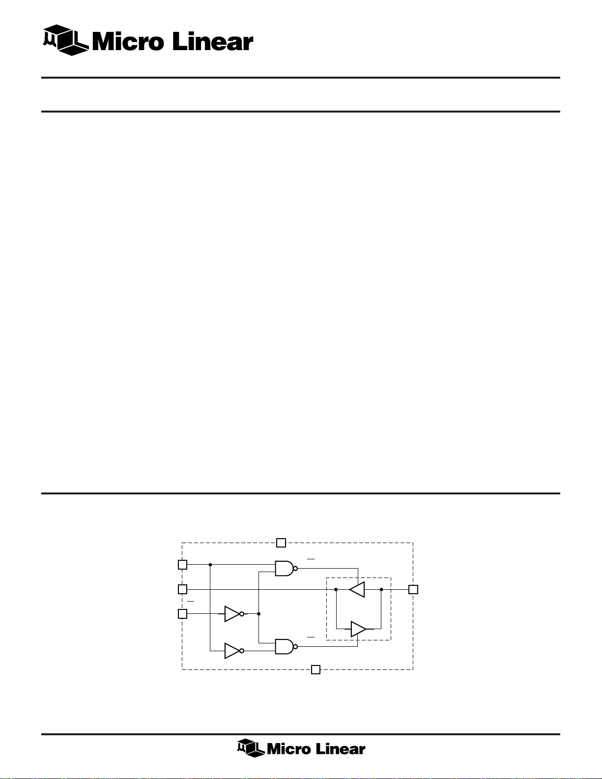
BLOCK DIAGRAM
DIR
Bi
OE
*This Part Is End Of Life As Of August 1, 2000
V
CC
OE
AB
Ai
OE
GND
Bi
BA
i=0 to 15
1
Page 2
ML65F16245
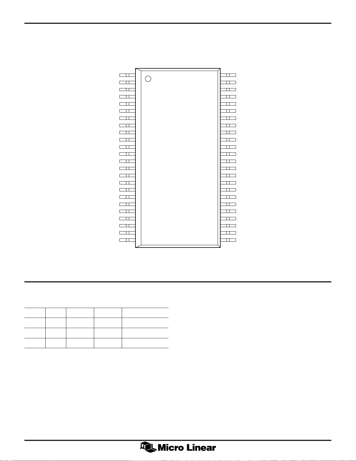
PIN CONFIGURATION
1DIR
1B0
1B1
GND
1B2
1B3
V
CC
1B4
1B5
GND
1B6
1B7
2B0
2B1
GND
2B2
2B3
V
CC
2B4
2B5
GND
2B6
2B7
2DIR
ML65F16245
48-Pin SSOP (R48)
48-Pin TSSOP (T48)
1
2
3
4
5
6
7
8
9
10
11
12
13
14
15
16
17
18
19
20
21
22
23
24
48
47
46
45
44
43
42
41
40
39
38
37
36
35
34
33
32
31
30
29
28
27
26
25
1OE
1A0
1A1
GND
1A2
1A3
V
CC
1A4
1A5
GND
1A6
1A7
2A0
2A1
GND
2A2
2A3
V
CC
2A4
2A5
GND
2A6
2A7
2OE
FUNCTION TABLE
(Each 8-bit section)
OE DIR Ai Bi FUNCTION
H X Z Z Disable
L L Output Input Bus B to Bus A
L H Input Output Bus A to Bus B
L = Logic Low, H = Logic High, X = Don’t Care, Z = High Impedance
i = 0 to 7
TOP VIEW
2
Page 3

PIN DESCRIPTION
ML65F16245
PIN NAME FUNCTION
1 1DIR Direction Select
2 1B0 Data Bus 1B
3 1B1 Data Bus 1B
4 GND Signal Ground
5 1B2 Data Bus 1B
6 1B3 Data Bus 1B
7V
8 1B4 Data Bus 1B
9 1B5 Data Bus 1B
10 GND Signal Ground
11 1B6 Data Bus 1B
12 1B7 Data Bus 1B
13 2B0 Data Bus 2B
14 2B1 Data Bus 2B
15 GND Signal Ground
16 2B2 Data Bus 2B
17 2B3 Data Bus 2B
18 V
19 2B4 Data Bus 2B
20 2B5 Data Bus 2B
21 GND Signal Ground
22 2B6 Data Bus 2B
23 2B7 Data Bus 2B
24 2DIR Direction Select
CC
CC
2.7V to 3.6V Supply
2.7V to 3.6V Supply
PIN NAME FUNCTION
25 2OE Output Enable
26 2A7 Data Bus 2A
27 2A6 Data Bus 2A
28 GND Signal Ground
29 2A5 Data Bus 2A
30 2A4 Data Bus 2A
31 V
32 2A3 Data Bus 2A
33 2A2 Data Bus 2A
34 GND Signal Ground
35 2A1 Data Bus 2A
36 2A0 Data Bus 2A
37 1A7 Data Bus 1A
38 1A6 Data Bus 1A
39 GND Signal Ground
40 1A5 Data Bus 1A
41 1A4 Data Bus 1A
42 V
43 1A3 Data Bus 1A
44 1A2 Data Bus 1A
45 GND Signal Ground
46 1A1 Data Bus 1A
47 1A0 Data Bus 1A
48 1OE Output Enable
CC
CC
2.7V to 3.6V Supply
2.7V to 3.6V Supply
3
Page 4

ML65F16245
ABSOLUTE MAXIMUM RATINGS
Absolute maximum ratings are those values beyond which
the device could be permanently damaged. Absolute
maximum ratings are stress ratings only and functional
device operation is not implied.
Storage Temperature Range ..................... –65°C to 150°C
Junction Temperature .............................................. 150°C
Lead Temperature (Soldering, 10sec) ...................... 150°C
Thermal Impedance (qJA) ..................................... 76°C/W
VCC............................................................................. 7V
DC Input Voltage............................. –0.3V to VCC + 0.3V
OPERATING CONDITIONS
AC Input Voltage (PW < 20ns) ................................ –3.0V
DC Output Voltage...................................–0.3V to 7VDC
Output Current, Source or Sink ............................. 180mA
Temperature Range ....................................... 0°C to 70°C
VIN Operating Range ...................................2.7V to 3.6V
ELECTRICAL CHARACTERISTICS
Unless otherwise specified, VIN = 3.3V, TA = Operating Temperature Range (Note 1).
SYMBOL PARAMETER CONDITIONS MIN TYP MAX UNITS
AC ELECTRICAL CHARACTERISTICS (C
t
PHL
, t
t
OE
Propagation Delay Ai to/from Bi 3.3V 1.35 1.7 2 ns
PLH
Output Enable Time OE to Ai/Bi 3.3V 5 ns
LOAD
= 50pF)
2.7V 1.25 1.9 2.5 ns
2.7V 6 ns
DIR to Ai/Bi 3.3V 5 n s
2.7V 6 n s
t
OD
T
C
DC ELECTRICAL CHARACTERISTICS (C
V
V
I
I
I
HI-Z
VICInput Clamp Voltage VCC = 3.6V, IIN = 18mA –0.7 –0.2 V
I
DYNAMIC
V
Output Disable Time OE to Ai/Bi 3.3V 5 ns
2.7V 6 ns
DIR to Ai/Bi 3.3V 5 n s
2.7V 6 n s
Output-to-Output Skew 300 ps
OS
Input Capacitance 8pF
IN
= 50pF, R
LOAD
Input High Voltage Logic high 2.0 V
IH
Input Low Voltage Logic low 0.8 V
IL
Input High Current Per pin, VIN = 3V 300 µA
IH
Input Low Current Per pin, VIN = 0V 300 µA
IL
Three-State Output Current VCC = 3.6V, 0 < VIN < V
Dynamic Transition Current Low to high transitions 80 mA
(FastBus Charge)
Output High Voltage VCC = 3.6V 2.4 3.4 V
OH
= Open)
LOAD
CC
High to low transitions 80 mA
VCC = 2.7V 2.25 2.35 V
5µA
V
I
CC
Note 1: Limits are guaranteed by 100% testing, sampling, or correlation with worst-case test conditions.
Output Low Voltage V
OL
Quiescent Power Supply Current V
= 3.6V and 2.7V 0.6 V
CC
= 3.6V, f = 0Hz, 3 µA
CC
inputs = VCC or 0V
4
Page 5

ML65F16245
100
80
60
(mA)
OL
I
40
20
0
0.4 1.2
0 0.8 1.6
VOL (V)
Figure 1a. Typical VOL vs. IOL for 3.3V VCC.
One Buffer Output
3.0
2.5
V
= 2.7V
CC
V
= 3.3V
CC
(ns)
PHL
t
2.0
1.5
1.0
0
–20
–40
–60
–80
–100
(mA)
OH
I
–120
–140
–160
–180
2
–200
2.0 2.4 3.42.8
1.8 2.2 2.6 3.63.2
VOH (V)
3.0
Figure 1b. Typical VOH vs. IOH for 3.3V VCC.
One Buffer Output
3.0
2.5
V
= 2.7V
CC
V
= 3.3V
CC
(ns)
PLH
t
2.0
1.5
1.0
0.5
0
050
25 75
LOAD CAPACITANCE (pF)
Figure 2a. Propagation Delay vs. Load Capacitance:
3.3V, 50MHZ
60
50
40
30
(mA)
CC
I
20
10
0
0 40 60 100
FREQUENCY (MHz)
75pF
50pF
30pF
8020
0.5
0
050
25 75
LOAD CAPACITANCE (pF)
Figure 2b. Propagation Delay vs. Load Capacitance:
2.7V, 50MHZ
60
50
75pF
40
30
(mA)
CC
I
20
10
0
0 40 60 100
FREQUENCY (MHz)
50pF
30pF
8020
Figure 3a. ICC vs. Frequency: VCC = VIN = 3.3V.
One Buffer Output
Figure 3b. ICC vs. Frequency: VCC = VIN = 2.7V.
One Buffer Output
5
Page 6

ML65F16245
FUNCTIONAL DESCRIPTION
1DIR
1OE
1OE
1OE
AB
BA
1B0
1B1
1B2
1B3
1B4
1B5
1B6
1A0
1A1
1A2
1A3
1A4
1A5
1A6
2DIR
2OE
2OE
2OE
AB
BA
2B0
2B1
2B2
2B3
2B4
2B5
2B6
2A0
2A1
2A2
2A3
2A4
2A5
2A6
1OE
1DIR
1A0
1B0
1A1
1B1
1B7
1A2
1B2
1A3
1B3
1A7
Figure 4. Logic Diagram
1A4
1A5
1A6
1A7
1B4
1B5
1B6
1B7
Figure 5. Logic Symbol
2A0
2B0
2A1
2B1
2A2
2B2
2A3
2B3
2A4
2B4
2B7
2A5
2B5
2A6
2B6
2A7
2A7
2OE
2DIR
2B7
6
Page 7

ARCHITECTURAL DESCRIPTION
ML65F16245
The ML65F16245 is a 16-bit (dual-octal) non-inverting bus
transceiver with 3-state outputs designed for 2.7V to 3.6V
VCC operation. This device is designed for asynchronous
communication between data buses. The ML65F16245
can be used as two 8-bit transceivers or as one 16-bit
transceiver and can be designated as Port-A bus and Port-B
bus. The Direction and Output Enable controls are
designed to operate these configurations. The direction
control pin (iDIR) controls the direction of the data flow.
The output enable pin (1OE, 2OE) overrides the direction
control and disables both ports.
Until now, these transceivers were typically implemented
in CMOS logic and made to be TTL compatible by sizing
the input devices appropriately. In order to buffer large
capacitances with CMOS logic, it is necessary to cascade
an even number of inverters, each successive inverter
larger than the preceding, eventually leading to an
inverter that will drive the required load capacitance at
the required frequency. Each inverter stage represents an
additional delay in the gating process because in order for
a single gate to switch, the input must slew more than
half of the supply voltage. The best of these 16-bit CMOS
buffers has managed to drive 50pF load capacitance with
a delay of 3ns.
Micro Linear has produced a 16-bit transceiver with a
delay less than 2ns (at 3.3V) by using a unique circuit
architecture that does not require cascade logic gates.
The basic architecture of the ML65F16245 is shown in
Figure 6. In this circuit, there are two paths to the output.
One path sources current to the load capacitance where
the signal is asserted, and the other path sinks current
from the output when the signal is negated.
The assertion path is the Darlington pair consisting of
transistors Q1 and Q2. The effect of transistor Q1 is to
increase the current gain through the stage from input to
output, to increase the input resistance and to reduce
input capacitance. During the transition state (the input
from low-to-high) the output transistor Q2 sources large
amount of current to quickly charge up a highly
capacitive load which in effect reduces the bus settling
time. This current is specified as I
DYNAMIC
.
The negation path is also the Darlington pair consisting of
transistor Q3 and transistor Q4. With M1 connecting to
the input of the Darlington pair, Transistor Q4 then sinks a
large amount of current during the input transition from
high-to-low.
Inverter X2 is a helpful buffer that not only drives the
output toward the upper rail but also pulls the output to
the lower rail.
There are a number of MOSFETs not shown in Figure 6.
These MOSFETs are used to 3-state the buffers.
V
OE
Q1
X1 X2
IN
M1
Q3
CC
Q2
Q4
Figure 6. One Buffer Cell of the ML65F16245
OUT
7
Page 8

ML65F16245
CIRCUITS AND WAVE FORMS
ML65F16245
DUT
V
IN
50pF
V
I
OUT
OUT
INPUT
OUTPUT
t
AND t
RISE
INPUT = 2ns
FALL
t
PLH
1.5V
t
PHL
VCC = 3V
0V
3V
1.5V
0V
CONTROL
INPUT
OUTPUT
LOW
OUTPUT
HIGH
Figure 7. Test Circuits for All Outputs
DISABLEENABLE
1.5V
t
OE
t
OE
t
OD
t
OD
Figure 9. Enable and Disable Times
VCC = 3V
3V
VOL + 0.3V
V
OL
VOH
VOH – 0.3V
0V
INPUT
OUTPUT1
OUTPUTi
i = 1 to 16
Figure 8. Propagation Delay
1.5V
1.5V
t
OS
Figure 10. Output Skew
1.5V
8
Page 9

PHYSICAL DIMENSIONS inches (millimeters)
Package: R48
48-Pin SSOP
0.620 - 0.630
(15.75 - 16.00)
48
ML65F16245
0.015 - 0.025
(0.38 - 0.64)
(4 PLACES)
0.088 - 0.092
(2.24 - 2.34)
1
PIN 1 ID
0.006 - 0.014
(0.15 - 0.36)
0.025 BSC
(0.63 BSC)
0.291 - 0.301
(7.39 - 7.65)
0.094 - 0.110
(2.39 - 2.79)
SEATING PLANE
Package: T48
48-Pin TSSOP
0.402 - 0.410
(10.21 - 10.41)
0.008 - 0.016
(0.20 - 0.41)
0º - 8º
0.024 - 0.040
(0.61 - 1.02)
0.005 - 0.010
(0.13 - 0.26)
0.031 - 0.039
(0.80 - 1.00)
PIN 1 ID
0.487 - 0.497
(12.37 - 12.63)
0.007 - 0.011
(0.17 - 0.27)
0.020 BSC
(0.50 BSC)
0.236 - 0.244
(6.00 - 6.20)
0.047 MAX
(1.20 MAX)
SEATING PLANE
0.319 BSC
0.002 - 0.006
(0.05 - 0.15)
(8.1 BSC)
0º - 8º
0.020 - 0.028
(0.50 - 0.70)
0.004 - 0.008
(0.10 - 0.20)
9
Page 10

ML65F16245
ORDERING INFORMATION
PART NUMBER TEMPERATURE RANGE PACKAGE
ML65F16245CR (Obsolete) 0°C to 70°C 48-Pin SSOP (R48)
ML65F16245CT (EOL) 0°C to 70°C 48-Pin TSSOP (T48)
© Micro Linear 1998. is a registered trademark of Micro Linear Corporation. All other trademarks are the property of their respective owners.
Products described herein may be covered by one or more of the following U.S. patents: 4,897,611; 4,964,026; 5,027,116; 5,281,862; 5,283,483; 5,418,502;
5,508,570; 5,510,727; 5,523,940; 5,546,017; 5,559,470; 5,565,761; 5,592,128; 5,594,376; 5,652,479; 5,661,427; 5,663,874; 5,672,959; 5,689,167; 5,714,897;
5,717,798; 5,742,151; 5,747,977; 5,754,012; 5,757,174; 5,767,653;. Japan: 2,598,946; 2,619,299; 2,704,176. Other patents are pending.
Micro Linear reserves the right to make changes to any product herein to improve reliability, function or design. Micro Linear does not assume any liability
arising out of the application or use of any product described herein, neither does it convey any license under its patent right nor the rights of others. The circuits
contained in this data sheet are offered as possible applications only. Micro Linear makes no warranties or representations as to whether the illustrated circuits
infringe any intellectual property rights of others, and will accept no responsibility or liability for use of any application herein. The customer is urged to consult
with appropriate legal counsel before deciding on a particular application.
10
2092 Concourse Drive
San Jose, CA 95131
Tel: (408) 433-5200
Fax: (408) 432-0295
www.microlinear.com
DS65F16245-01
 Loading...