

Page 1
February 1997
ML6599*
Hot-Insertable Active SCSI Terminator
GENERAL DESCRIPTION
The ML6599 BiCMOS 9 line SCSI terminator provides
active termination in SCSI systems using single ended
drivers and receivers. Active SCSI termination helps to
effectively control analog transmission line effects such as
ringing, noise, crosstalk, and ground bounce. In addition,
the ML6599 provides support for hot-insertability on the
SCSI bus.
The ML6599 provides a V-I characteristic optimized to
minimize transmission line effects during both signal
negation and assertion using a MOSFET-based
architecture. The desired V-I characteristic is achieved by
trimming one resistor in the control block. Internal
clamping controls signal assertion transients and provides
current sink capability to handle active negation driver
overshoots above 2.85V. It provides a 2.85V reference
through an internal low dropout (1V) linear regulator.
The ML6599 also provides a disconnect function which
effectively removes the terminator from the SCSI bus. The
disconnect mode capacitance is typically less than 5pF
FEATURES
■ Fully monolithic IC solution providing active
termination for 9 lines of the SCSI bus
■ Provides on board support for hot-insertability on the
SCSI bus
■ Low dropout voltage (1V) linear regulator, trimmed for
accurate termination current
■ Output capacitance typically < 5pF
■ Disconnect mode — logic pin to disconnect terminator
from the SCSI bus, <100µA
■ Current sinking — can sink current in excess of 10mA
per line to handle active negation driver overshoots
above 2.85V
■ Negative clamping on all lines to handle signal
assertion transients
■ Regulator can source 200mA and sink 100mA while
maintaining regulation
■ Current limit & thermal shutdown protection
per line. Current limiting and thermal shutdown
protection are also included. *Some Packages Are Obsolete
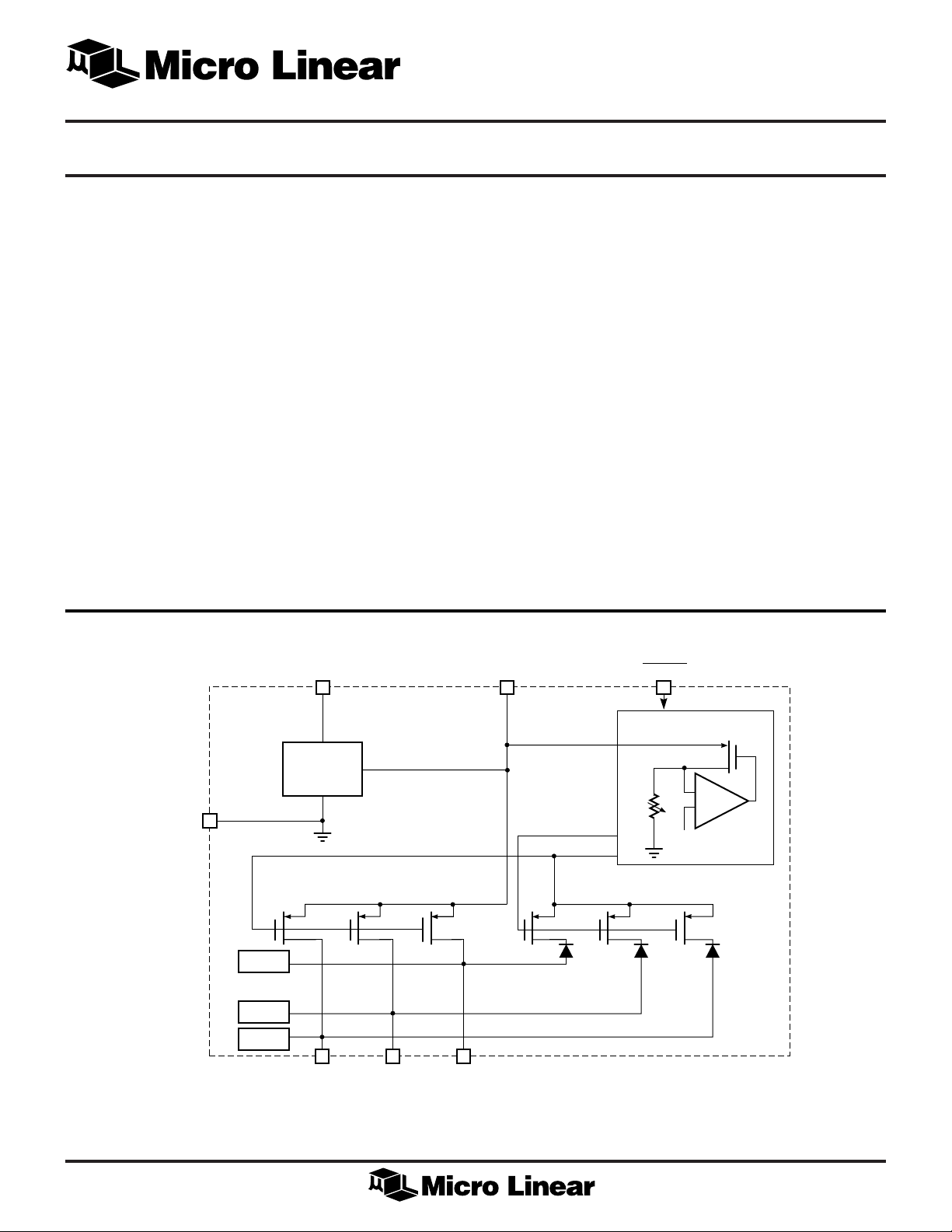
BLOCK DIAGRAM
GND
NCLAMP = Negative Clamp
NCLAMP
. . .
NCLAMP
NCLAMP
TERMPWR
LINEAR
REGULATOR
1V DROPOUT
MOSFETs WITH I
9 TERMINATION LINES
. . .
L2 L9L1
2.85V
MAX
. . .
= 24mA
R
TRIM
DISCNKT
2.85V
V
REF
CONTROL
BLOCK
V
REF
. . .
. . .
1
Page 2
ML6599
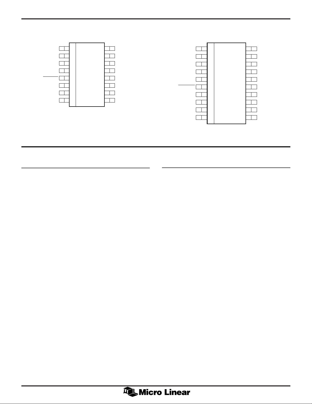
PIN CONFIGURATION
20-Pin TSSOP16-Pin SOIC
TERMPWR
NC
NC
GND
DISCNKT
NC
1
2
3
4
5
6
L1
L2
7
8
16
15
14
13
12
11
10
9
L9
L8
L7
V
REF
L6
L5
L4
L3
PIN DESCRIPTION
NAME DESCRIPTION
TERMPWR Termination Power. Should be connected
to the SCSI TERMPWR line. A 10µF
tantalum local bypass capacitor is
recommended per system, as shown in
the application diagram
L1 Signal Termination 1. SCSI Bus line 1
L2 Signal Termination 2. SCSI Bus line 2
L3 Signal Termination 3. SCSI Bus line 3
L4 Signal Termination 4. SCSI Bus line 4
L5 Signal Termination 5. SCSI Bus line 5
L6 Signal Termination 6. SCSI Bus line 6
L7 Signal Termination 7. SCSI Bus line 7
L8 Signal Termination 8. SCSI Bus line 8
L9 Signal Termination 9. SCSI Bus line 9
TERMPWR
NC
GND
NC
DISCNKT
NC
HS
HS
1
2
3
4
5
6
7
8
L1
L2
9
10
20
19
18
17
16
15
14
13
12
11
L9
L8
HS
L7
V
L6
L5
L4
HS
L3
REF
NAME DESCRIPTION
V
REF
2.85V
Output. External decoupling
REF
with a 10µF tantalum in parallel with a
0.1µF ceramic capacitor is
recommended, as shown in the
application diagram.
DISCNKT Disconnect Terminator. Logic input to
disconnect the terminator from the bus
when the SCSI device no longer needs
termination due to not being the last
device on the bus or otherwise. Active
low input.
GND Ground. Signal ground (0V)
HS Heat Sink Ground. Should be
connected to GND.
NOTE : The DISCNKT line has a 200kΩ internal pullup resistor connected to the
supply. This pin should be left floating for normal operation and should
be connected to ground to enable the function.
2
Page 3

ML6599
ABSOLUTE MAXIMUM RATINGS
Signal Line Voltage .................. –0.3 to TERMPWR + 0.3V
Regulator Output Current ......................... –100 to 300mA
OPERATING CONDITIONS
TERMPWR Voltage ........................................ 4V to 5.25V
Operating Temperature ................................. 0°C to 70°C
TERMPWR Voltage ........................................... –0.3 to 7V
Storage Temperature................................. –65°C to 150°C
Soldering Temperature ................................ 260°C for 10s
Thermal Impedance (θ
)
JA
SOIC ................................................................ 95°C/W
TSSOP ............................................................ 110°C/W
ELECTRICAL CHARACTERISTICS
Unless otherwise stated, these specifications apply for 4V ≤ TERMPWR ≤ 5.25V, and TA = 0°C to 70°C (Note 1)
PARAMETER CONDITIONS MIN TYP MAX UNITS
Supply
TERMPWR Supply Current L1–L9 = open, DISCNKT = open 4.5 5.5 mA
L1–L9 = 0.2 V, DISCNKT = open 225 250 mA
Disconnect Mode Current DISCNKT = 0 (active) 75 100 µA
DISCNKT
Input Low Voltage 1.0 V
Input High Voltage TERMPWR – 1.0 V
Output
Output High Voltage Measuring each signal line 2.8 2.85 2.9 V
while other eight are high
Output Current V
(Normal Mode) line while the other eight are high
Hot Insertion Peak Current TERMPWR = 0V, V
Output Clamp Level I
Sinking Current (per line) V
Output Capacitance L1 thru L9, DISCNKT = 0 4 5 pF
(Micro Linear Method) 2V
Output Capacitance L1 thru L9, DISCNKT = 0 6 7 pF
(X3T9.2/855D method) 0.4V
Regulator
Output Voltage Sourcing 0-200mA 2.8 2.85 2.9 V
Sinking Current V = 3.5V 125 150 mA
Short Circuit Current V
Dropout Voltage L1–L9 = 0.2V 1.0 1.2 V
Thermal Shutdown 170 °C
= 0.2V, Measuring each signal 20 24 mA
OUT
= 0V 1 2 µA
Any signal line (L1–L9) at 2.85V
= –30mA (Note 2) –0.15 0 0.15 V
OUT
= 3.3V (per line) 10 12 mA
OUT
100kHz square wave
P-P
applied biased at 1V D.C.
, 1MHz square wave
P-P
applied biased at 0.5V D.C.
Sinking 0-100mA 2.8 2.85 2.9 V
= 0V 150 mA
REF
V
= 5V 300 mA
REF
REF
Note 1: Limits are guaranteed by 100% testing, sampling, or correlation with worst case test conditions.
3
Page 4

ML6599
FUNCTIONAL DESCRIPTION
SCSI terminators are used to decrease the transmission
line effects of SCSI cable. Termination must be provided
at the beginning and end of the SCSI bus to ensure that
data errors due to reflections on the bus are eliminated.
With the increasing use of higher data rates and cable
lengths in SCSI subsystems, active termination has
become necessary. Active termination also minimizes
power dissipation and can be activated or deactivated
under software control, thus eliminating the need for end
user intervention. The V-I characteristics of popular SCSI
termination schemes are shown in Figure 1. Theoretically,
the desired V-I characteristics are the Boulay type for
signal assertion (high to low) and the ideal type for signal
negation (low to high). The ML6599 with its MOSFETbased nonlinear termination element provides the most
optimum V-I characteristics for both signal assertion and
negation.
V
2.85V
2.7V
2.5V
BOULAY
220/330
0.2V
TERMINATOR (SOURCE)
DRIVER (SINK)
Figure 1. V-1 Characteristics of Various
SCSI Termination Schemes
ML6599
20mA
40mA
IDEAL
24mA
48mA
The ML6599 provides active termination for 9 signal lines,
thus accommodating basic SCSI which requires 9 lines to
be terminated. When used with the ML6599, wide SCSI,
which requires 27, 36 or 45 lines to be terminated, can
also be accommodated. The ML6599 integrates an
accurate voltage reference (1V dropout voltage) and 9
MOSFET-based termination lines. A single internal resistor
is trimmed to tune the V-I characteristic of the MOSFETs.
The voltage reference circuit produces a precise 2.85V
level and is capable of sourcing 24mA into each of the
nine terminating lines when low (active). When the signal
line is negated (driver turns off), the terminator pulls the
signal line back to 2.85V. The regulator will source
200mA and sink 100mA while maintaining regulation of
2.85V.
The ML6599 SCSI terminator provides an active low
control signal (DISCNKT) which has an internal 200kΩ
pull-up resistor. The DISCNKT input isolates the ML6599
from the signal lines and effectively removes the
terminator from the SCSI bus with a disconnect mode
current of less than 100µA when pulled low. In addition,
the ML6599 provides for negative clamping of signal
transients and also supports current sink capability in
excess of 10mA per signal line to handle active negation
driver overshoot above 2.85V, a common occurrence with
SCSI transceivers.
Disconnect mode capacitance is a very critical parameter
in SCSI systems. The ML6599 provides a capacitance
contribution of only 5pF.
HOT-INSERTABILITY
“Hot” insertion of a SCSI device refers to the act of
plugging a SCSI device which is initially unpowered into
a powered SCSI bus. The SCSI device subsequently draws
power from the TERMPWR line during its startup routine
and thereafter. “Hot” removal refers to the act of removing
a powered SCSI device from a powered SCSI bus. A
I
device which performs both tasks with no physical
damage to itself or other devices on the bus, nor which
alters the existing state of the bus by drawing excessive
currents, is termed “hot-swappable.”
The ML6599 hot-insertable SCSI terminator typically
draws 1µA from any given output line (L1–L9) during a
hot-insertion/removal procedure, thereby protecting itself
and preserving the state of the bus. The low insertion
current is achieved by effectively shorting the gate to drain
of the output PMOS device until the 2.85V reference
(V
) has powered up. A second PMOS in series with a
REF
Schottky diode is used as the shorting bypass device. After
V
reaches a sufficient level, the bypass device is turned
REF
off and the part operates normally. Figure 2 gives an
application diagram showing a typical SCSI bus
configuration. To ensure proper operation, the TERMPWR
pin must be connected to the SCSI TERMPOWER line. As
outlined in Annex G of the ANSI SCSI-3 Parallel Interface
Specification (X3T9.2/855D), “The SCSI bus termination
shall be external to the device being inserted or removed.”
In other words, any terminator connected to a device
4
Page 5

ML6599
being hot-inserted/removed should be inactive
(accomplished by grounding the DISCNKT pin in the case
of the ML6599). If the terminator being inserted/removed
were in the active state, at some point in time the bus
would be terminated by either 1 or 3 terminators. In either
case, data integrity on the bus will be compromised.
Figure 2 gives an application diagram showing a typical
SCSI bus configuration. To ensure proper operation, the
TERMPWR pin must be connected to the SCSI
TERMPOWER line. Each ML6599 requires parallel 0.1µF
and 10µF capacitors connected between the V
REF
and
GND pins and the TERMPOWER line needs a 10µF
bypass capacitor at each node in the system.
In an 8-bit wide SCSI bus arrangement (“A” Cable),
two ML6599s would be needed at each end of the SCSI
cable in order to terminate the 9 active signal lines.
16-bit wide SCSI would use three ML6599s, while 32-bit
wide SCSI bus would require five ML6599s.
In a typical SCSI subsystem, the open collector driver in
the SCSI transceiver pulls low when asserted. The
termination resistance serves as the pull-up when negated.
Figure 2 also shows a typical cable response to a pulse.
The receiving end of the cable will exhibit a single time
delay. When negated, the initial step will reach an
intermediate level (V
). With higher SCSI data rates,
STEP
sampling could occur during this step portion. In order to
get the most noise margin, the step needs to be as high as
possible to prevent false triggering. For this reason the
regulator voltage and the resistor defining the MOSFET
characteristic are trimmed to ensure that the IO is as close
as possible to the SCSI maximum current specification.
V
is defined as:
STEP
V
= VOL + (I
STEP
O
× Z
)
O
where VOL is the driver output low voltage, IO is the
current from the receiving terminator, and ZO is the
characteristic impedance of the cable.
This is a very important characteristic that the terminator
helps to overcome by increasing the noise margin and
boosting the step as high as possible.
0.1µF
10µF
V
GND
SCSI XCVR
SCSI XCVR
ML6599
TERMPWR
REF
DISCNKT
. . .
L9 L2 L1
. . .
TERMPWR LINE
V
REG
SCSI CABLE
V
V
REG
STEP
ML6599
TERMPWR
DISCNKT
. . .
V
REF
GND
L9L1 L2
SCSI XCVR
. . .
0.1µF
10µF
V
OL
t
LINE ASSERTED LINE NEGATED
D
t
D
Figure 2. Application Diagram Showing Typical SCSI Bus Configuration with the ML6599
5
Page 6

ML6599
TRANSIENT RESPONSE (ACTUAL)
(Approximately 110Ω, 10 feet long, ribbon cable stock)
2.0V
0.8V
V1(2) = 796.9mV V2(2) = 2.0V ∆V(2) = 1.203V
2
6
Page 7

PHYSICAL DIMENSIONS inches (millimeters)
20-Pin TSSOP
0.251 - 0.262
(6.38 - 6.65)
20
ML6599
Package: T20
0.033 - 0.037
(0.84 - 0.94)
1
16
PIN 1 ID
0.008 - 0.012
(0.20 - 0.30)
0.400 - 0.414
(10.16 - 10.52)
0.026 BSC
(0.65 BSC)
0.169 - 0.177
(4.29 - 4.50)
0.043 MAX
(1.10 MAX)
SEATING PLANE
0.246 - 0.258
(6.25 - 6.55)
0.002 - 0.006
(0.05 - 0.15)
Package: S16W
16-Pin Wide SOIC
0º - 8º
0.020 - 0.028
(0.51 - 0.71)
0.004 - 0.008
(0.10 - 0.20)
0.024 - 0.034
(0.61 - 0.86)
(4 PLACES)
0.090 - 0.094
(2.28 - 2.39)
1
PIN 1 ID
0.050 BSC
(1.27 BSC)
0.012 - 0.020
(0.30 - 0.51)
0.291 - 0.301
(7.39 - 7.65)
0.095 - 0.107
(2.41 - 2.72)
SEATING PLANE
0.398 - 0.412
(10.11 - 10.47)
0.005 - 0.013
(0.13 - 0.33)
0º - 8º
0.022 - 0.042
(0.56 - 1.07)
0.009 - 0.013
(0.22 - 0.33)
7
Page 8

ML6599
ORDERING INFORMATION
PART NUMBER TEMPERATURE RANGE PACKAGE
ML6599CS0°C to 70°C16-pin SOIC (S16W) (Obsolete)
ML6599CT 0°C to 70°C 20-pin TSSOP (T20)
© Micro Linear 1997 is a registered trademark of Micro Linear Corporation
Products described herein may be covered by one or more of the following patents: 4,897,611; 4,964,026; 5,027,116; 5,281,862; 5,283,483; 5,418,502; 5,508,570; 5,510,727; 5,523,940; 5,546,017;
5,559,470; 5,565,761; 5,594,376. Other patents are pending.
Micro Linear reserves the right to make changes to any product herein to improve reliability, function or design.
Micro Linear does not assume any liability arising out of the application or use of any product described herein,
neither does it convey any license under its patent right nor the rights of others. The circuits contained in this
data sheet are offered as possible applications only. Micro Linear makes no warranties or representations as to
whether the illustrated circuits infringe any intellectual property rights of others, and will accept no responsibility
or liability for use of any application herein. The customer is urged to consult with appropriate legal counsel
before deciding on a particular application.
8
2092 Concourse Drive
San Jose, CA 95131
Tel: 408/433-5200
Fax: 408/432-0295
DS6599-01
 Loading...