

Page 1
www.fairchildsemi.com
ML6554
3A Bus Termination Regulator
Features
• Can source and sink up to 3A, no heat sink required
• Integrated Power MOSFETs
• Generates termination voltages for DDR SDRAM,
SSTL-2 SDRAM, SGRAM, or equivalent memories
• Generates termination voltages for active termination
schemes for DDR SDRAM, GTL+, Rambus, VME,
LV-TTL, HSTL, PECL and other high speed logic
•V
• Separate voltages for V
• Buffered V
•V
input available for external voltage divider
REF
output
REF
of ±3% or less at 3A
OUT
CCQ
and PV
DD
• Minimum external components
• Shutdown for standby or suspend mode operation
• 0° to +70°C and -40° to +85°C temperature ranges
available
• Thermal Shutdown ≈ 130ºC
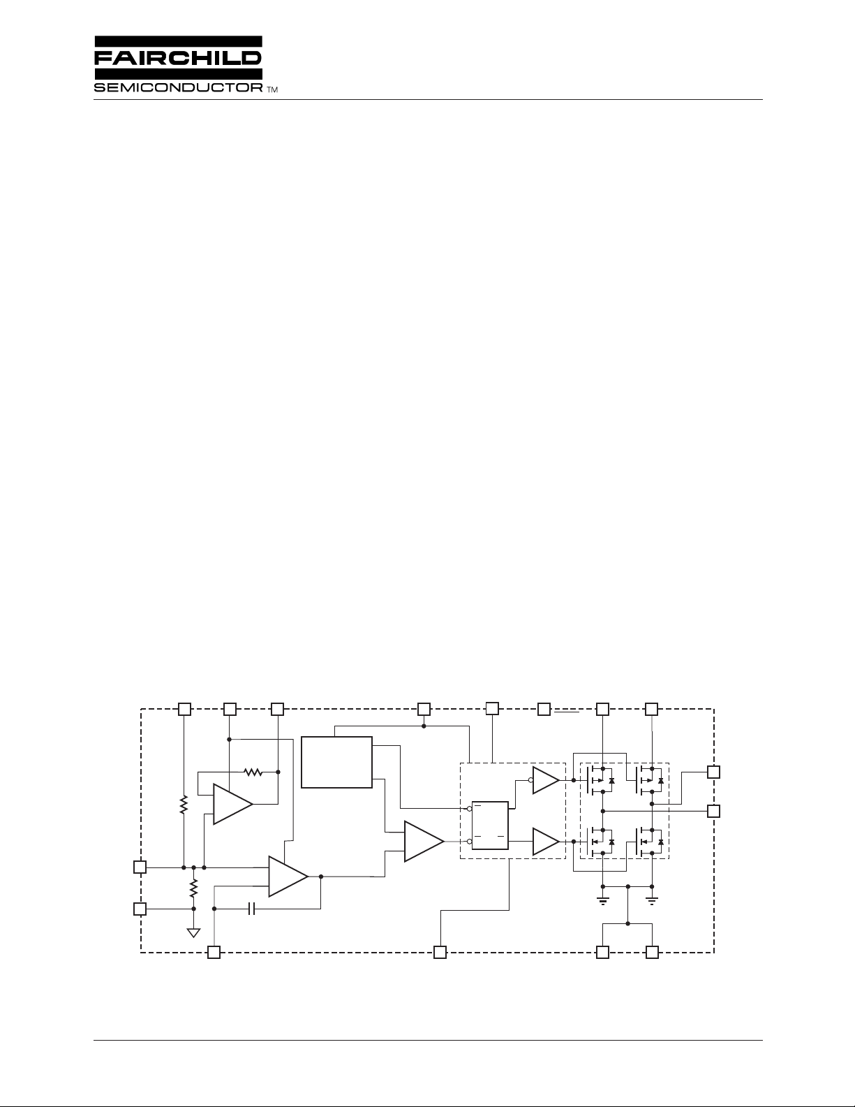
Block Diagram
Description
The ML6554 switching regulator is designed to convert voltage supplies ranging from 2.3V to 4V into a desired output
voltage or termination voltage for various applications. The
ML6554 can be implemented to produce regulated output
voltages in two different modes. In the default mode, when
the V
the voltage applied to V
to produce various user-defined voltages by forcing a voltage
on the VREF
the input VREF
ble of sourcing or sinking up to 3A of current while regulating an output V
The ML6554, used in conjunction with series termination
resisitors, provides an excellent voltage source for active
termination schemes of high speed transmission lines as
those seen in high speed memory buses and distributed
backplane designs. The voltage output of the regulator can
be used as a termination voltage for other bus interface
standards such as DDR SDRAM, SSTL, CMOS, Rambus
GTL+, VME, LV-CMOS, LV-TTL, HSTL and PECL.
pin is open, the ML6554 output voltage is 50% of
REF
pin. In this case, the output voltage follows
IN
voltage. The switching regulator is capa-
IN
voltage to within 3% or less.
TT
. The ML6554 can also be used
CCQ
™
,
11
13
200kΩ
VREF
200kΩ
AGND
D
GND
9
S
R
12
V
DD
Q
Q
SHDN
2
4 58
PV
P
GND1
DD1
7
PV
DD2
V
L1
(V
)
OUT
3
6
V
L2
(V
)
OUT
P
GND2
15
IN
V
CCQ
10
16
–
+
V
V
FB
AV
REF
14
CC
BUFFER
+
–
VREF
OUT
OSCILLATOR/
RAMP
GENERATOR
ERROR AMP
1
V
DD
–
+
RAMP
COMPARATOR
REV. 1.1.3 3/8/02
Page 2
2
ML6554 PRODUCT SPECIFICATION
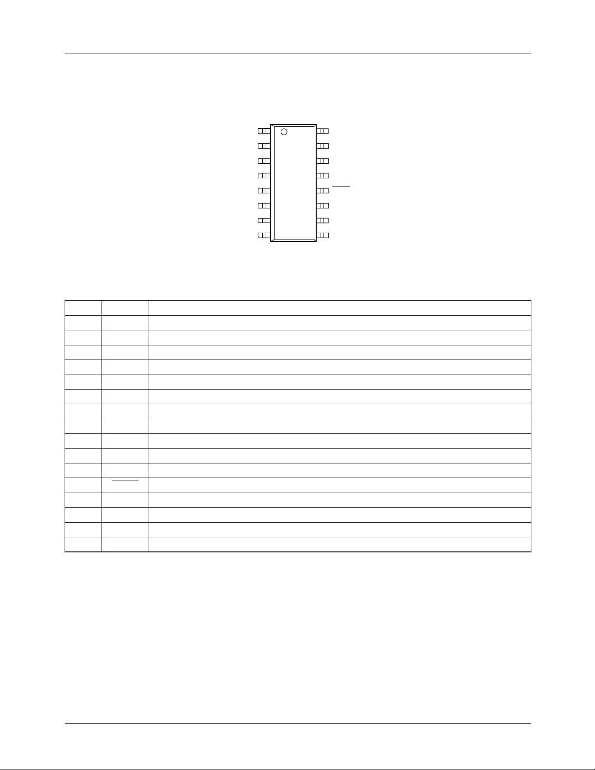
Pin Configuration
ML6554
16-Pin PSOP (U16)
Pin Description
Pin Name Function
1V
2PV
3V
4P
5P
6V
7PV
8D
9V
10 V
11 VREF
12 SHDN Shutdown active low. CMOS input level
13 AGND Ground for internal reference voltage divider
14 VREF
15 V
16 AV
DD
DD1
L1
GND1
GND2
L2
DD2
GND
DD
FB
OUT
CCQ
CC
PV
P
GND1
P
GND2
PV
D
V
DD
DD1
V
V
DD2
GND
L1
L2
1
2
3
4
5
6
7
8
TOP VIEW
Digital supply voltage
Voltage supply for internal power transistors
Output voltage/ inductor connection
Ground for output power transistors
Ground for output power transistors
Output voltage/inductor connection
Voltage supply for internal power transistors
Digital ground
Digital supply voltage
Input for external compensation feedback
Input for external reference voltage
IN
Reference voltage output
Voltage reference for internal voltage divider
Analog voltage supply
AV
16
15
14
13
12
11
10
9
CC
V
CCQ
VREF
AGND
SHDN
VREF
V
FB
V
DD
OUT
IN
REV. 1.1.3 3/8/02
Page 3
∆
PRODUCT SPECIFICATION ML6554
Absolute Maximum Ratings
Absolute maximum ratings are those values beyond which the device could be permanently damaged. Absolute maximum
ratings are stress ratings only and functional device operation is not implied.
Parameter Min. Max. Units
PV
DD
Voltage on Any Other Pin GND – 0.3 V
Average Switch Current (I
) 3.0 A
AVG
4.5 V
+ 0.3 V
IN
Junction Temperature 150 °C
Storage Temperature Range -65 150 °C
Lead Temperature (Soldering, 10 sec) 150 °C
Thermal Resistance ( θ
)(Note 2) 2 °C/W
JC
Output Current, Source or Sink 3.0 A
Operating Conditions
Parameter Min. Max. Units
Temperature Range, CU suffix 0 70 °C
Temperature Range, IU suffix -40 +85 °C
PV
Operating Range 2.0 4.0 V
DD
V
Operating Range 1.4 4.0 V
CCQ
Electrical Characteristics
Unless otherwise specified, AV
Symbol Parameter Conditions Min. Typ. Max. Units
Switching Regulator
V
TT
Output Voltage, SSTL_2
(See Figure 1)
VREF
Z
IN
Internal Resistor Divider I
OUT
V
Reference Pin Input
REF
Impedance
Switching Frequency 650 kHz
V
OFFSET
Offset Voltage V
Supply
I
Q
Quiescent Current I
Buffer
I
REF
Notes
1. Limits are guaranteed by 100% testing, sampling, or correlation with worst-case test conditions.
2. Infinite heat sink
Output Load Current 3 mA
= V
CC
– VREF
TT
DD
= PV
OUT
= 3.3V ±10%, TA = Operating Temperature Range (Note 1)
DD
I
= 0,
OUT
V
= open
REF
I
= ±3A,
OUT
V
= open
REF
= 0 V
OUT
AV
= 2.5V No Load V
CC
= 0, no load
OUT
V
= 2.5V
CCQ
V
= 2.3V 1.12 1.15 1.18 V
CCQ
V
= 2.5V 1.22 1.25 1.28 V
CCQ
V
= 2.7V 1.32 1.35 1.38 V
CCQ
V
= 2.3V 1.09 1.15 1.21 V
CCQ
V
= 2.5V 1.19 1.25 1.31 V
CCQ
V
= 2.7V 1.28 1.35 1.42 V
CCQ
= 2.3V 1.139 1.15 1.162 V
CCQ
V
= 2.5V 1.238 1.25 1.263 V
CCQ
V
= 2.7V 1.337 1.35 1.364 V
CCQ
V
= 0 100 k Ω
CCQ
= 2.5 –20 20 mV
CCQ
I
VCCQ
I
AVCC
I
SD 0.2 0.5 mA
AVCC
I
VDD
I
SD 0.2 1.0 mA
VDD
I
PVDD
610µA
0.5 1.0 mA
0.25 1.0 mA
100 250 µA
REV. 1.1.3 3/8/02
3
Page 4
4
ML6554 PRODUCT SPECIFICATION
Functional Description
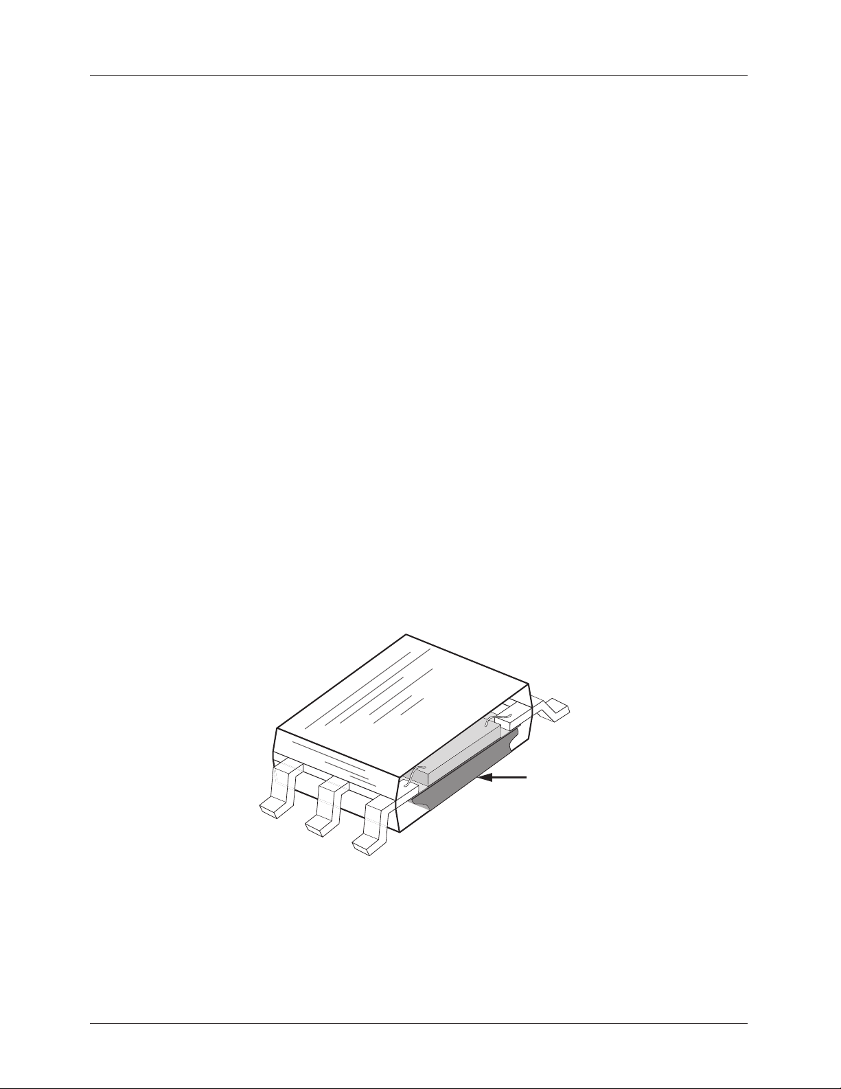
This switching regulator is capable of sinking and sourcing
3A of current without an external heatsink. The ML6554
uses a power surface mount package (PSOP) that includes
an integrated heat slug. The heat can be piped through the
bottom of the device and onto the PCB (Figure 1).
The ML6554 integrates two power MOSFETs that can be
used to source and sink 3A of current while maintaining a
tight voltage regulation. Using the external feedback, the
output can be regulated well within 3% or less, depending on
the external components chosen. Separate voltage supply
inputs have been added to accommodate applications with
various power supplies for the databus and power buses, see
Figure 2.
Outputs
The output voltage pins (V
address, or clock lines via an external inductor. See the
Applications section for recommendations. Output voltage
is determined by the V
Inputs
The input voltage pins (V
output voltages (V
the VREF
V
input. V
CCQ
databus.
IN
L1
pin is floating, the output voltage is 50% of the
can be the reference voltage for the
CCQ
, V
) are tied to the databus,
L1
L2
or VREF
CCQ
or VREF
CCQ
or V
) . In the default mode, where
L2
inputs.
IN
) determine the
IN
Output voltage can also be selected by forcing a voltage at
the VREF
voltage at the VREF
pin. In this case, the output voltage follows the
IN
input. Simple voltage dividers can be
IN
used this case to produce a wide variety of output voltages
between 0.7V and V
DD
–0.7V.
VREF Input and Output
The VREF
outputs (Inputs section, above). The VREF
output pin that is driven by a small output buffer to provide
the V
buffer is capable of driving several output loads. The output
buffer can handle 3mA.
input can be used to force a voltage at the
IN
signal to other devices in the system. The output
REF
OUT
pin is an
Other Supply Voltages
Several inputs are provide for the supply voltages: PV
PV
, AV
DD1
, and VDD.
CC
and PV
provide the power supply to the
DD2
DD2
The PV
power MOSFETs. VDD provides the voltage supply to the
digital sections, while AVCC supplies the voltage for the
analog sections. Again, see the Applications section for
recommendations.
DD1
,
Feedback Input
The VFB pin is an input that can be used for closed loop
compensation. This input is derived from the voltage output.
See application section for recommendation.
Figure 1. Cutaway view of PSOP Package
HEAT SLUG
REV. 1.1.3 3/8/02
Page 5
PRODUCT SPECIFICATION ML6554
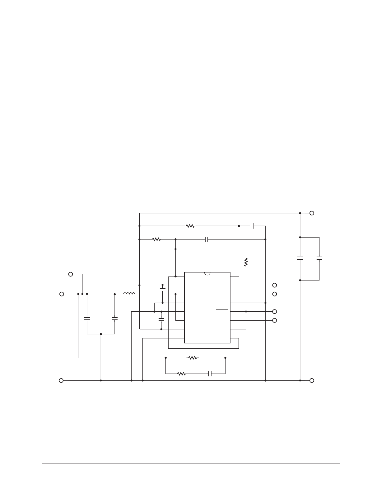
Applications
Using the ML6554 for SSTL Bus Termination
The circuit schematic in Figure 2 shows a recommended
approach for constructing a bus terminating solution for an
SSTL-2 bus. This circuit can be used in PC memory and
Graphics memory applications as shown in Figures 4 and 5.
Note that the ML6554 can provide the voltage reference
(V
) and terminating voltages (VTT). Using the layout
REF
as shown in Figures 6, 7, and 8, and measuring the VTT
performance using the test setup as described in Figure 9,
the ML6554 delivered a V
(see Figure 10). Table 1 provides a recommended parts list
for the circuit in Figure 2.
± 20mV for 1A to 3A loads
TT
Power Handling Capability of the PSOP
Package
Using the board layout shown in Figures 6, 7, and 8; soldering the ML6554 to the board at zero LFPM the temperature
around the package measured 55ºC for 3A loads. Note that a
1 ounce copper plane was used in the board construction.
Airflow is not likely to be needed in the operation of this
device (assuming a board layout similar to that described
above). The power handling performance of the PSOP
package is shown by a study of the package manufacturer for
various airflow vs. θ
conditions in Figure 11.
JA
Bus Termination Solutions for Others Buses
Table 3 provides a summary of various bus termination V
& VTT requirements. The ML6554 can be used for those
applications.
R2 100Ω
C8 0.1µF
REF
2.5V TO 4V
TPI
V
TT
TO SDRAMS
C1
820µF
F2V
OS-CON
L1 3.3µH
C2
0.1µF
R1 100Ω
C3 0.1µF
C4 0.1µF
1
V
2
PV
3
V
4
P
5
P
6
V
7
PV
8
D
R4 100kΩ
R5 1kΩ
Figure 2.
C9 0.1µF
ML6554
DD
DD1
L1
GND1
GND2
L2
DD2
GND
U1
VREF
C7 1nF
AV
V
CCQ
OUT
AGND
SHDN
VREF
V
OUT
IN
C5
330µF 330µF
R3
100kΩ
16
CC
15
14
13
12
11
IN
10
V
FB
9
DD
V
CCQ
VREF
SHDN
VREF
C6
GNDGND
REV. 1.1.3 3/8/02 5
Page 6

ML6554 PRODUCT SPECIFICATION
2.5V TO 4V
C3 10µF
L1 3.3µH
C2
0.1µF
Figure 3. Alternate Application Circuit
V
TT
TO SDRAMS
C1
820µF
F2V
OS-CON
An alternate application circuit for the ML6554 is shown in
Figure 3. The number of external components is reduced
compared to the circuit in Figure 2. This is achieved by
replacing four, 0.1µF bypass capacitors with one, low ESR,
10µF ceramic capacitor placed right next to U1. Two 100Ω
resistors are also eliminated. High value, surface-mount
1
2
3
4
5
6
7
8
R1 100kΩ
R2 1kΩ
C5
330µF 330µF
OUT
IN
V
DD
PV
V
L1
P
GND1
P
GND2
V
L2
PV
D
GND
DD1
DD2
U1
ML6554
VREF
C4 1nF
AV
V
CCQ
AGND
SHDN
VREF
CC
OUT
V
FB
V
DD
R3
100kΩ
16
15
14
13
12
11
IN
10
9
V
CCQ
VREF
SHDN
VREF
MLC capacitors were not available when the original application circuit (Figure 2) was developed. Both application
circuits offer the same electrical performance but that shown
in Figure 2 has a reduced bill-of-materials. Table 2 shows the
recommended parts list for the circuit of Figure 3.
C6
GNDGND
6 REV. 1.1.3 3/8/02
Page 7

PRODUCT SPECIFICATION ML6554
168/184/208-PIN DIMM CONNECTORS
AND SDRAM/SGRAM MODULES
TERMINATION
RESISTORS
PC CHIP SET
NORTHBRIDGE
DATA LINE, CLOCK LINES,
ADDRESS LINES, CONTROL LINES
TERMINATION
RESISTORS
VREF
Figure 4. Complete Termination Solution PC Main Memory (PC Motherboard)
SO DIMM
AND MODULES
TERMINATION
RESISTORS
VTT
ML6554
SGRAM
3D
GRAPHIC CHIP
DATA LINE, CLOCK LINES,
ADDRESS LINES, CONTROL LINES
TERMINATION
RESISTORS
VOLTAGE
REGULATOR
5V OR 3.3V
2.5V
AGP/PCI BUS
VREF
ML6554
VTT
Figure 5. Complete Termination Solution Graphics Memory Bus – AGP Graphics Cards
REV. 1.1.3 3/8/02 7
Page 8

ML6554 PRODUCT SPECIFICATION
Figure 6. Top Silk
Figure 7. Top Layer Figure 8. Bottom Layer
8 REV. 1.1.3 3/8/02
Page 9

PRODUCT SPECIFICATION ML6554
3.3V POWER
SUPPLY
VA
V
CCQ
SUPPLY
VA
ACTIVE
CLAMP
V
CCQ
Figure 9. Test Circuit Setup
V
ML6554
EVAL
GND
DD
V
TT
CURRENT SOURCE/SINK
POWER SUPPLY
I
TT
VTT VARIANCE WITH VDD@ITT (V
1.29
1.28
(V)
TT
V
1.27
1.26
2.0 2.5 3.0 4.03.5
TESTED WITH EVAL PCB
VDD (V)
Figure 10. VTT Performance for SSTL-2 Bus
CCQ
2.5V)
I
TT
3A SINKING
2A SINKING
1A SINKING
0A SINKING
3A SOURCING
2A SOURCING
1A SOURCING
REV. 1.1.3 3/8/02 9
Page 10

ML6554 PRODUCT SPECIFICATION
Table 1. Recommend Parts List for SSTL-2 Termination Circuit in Figure 2.
Item Qty Description Manufacturer / Part Number Designator
Resistors
1 2 100Ω1210 SMD Panasonic/ERJ-8ENF1000V R1, R2
211kΩ 1210 SMD Panasonic/ERJ-8ENF1001V R5
3 2 100kΩ1210 SMD Panasonic/ERJ-8ENF1003V R3, R4
Capacitors
4 3 0.1µF 1210 Film SMD Panasonic/ECV3VB1E104K
Panasonic/ECU-V1H104KBW
5 1 820µF 2V Solid Elect. SMD Sanyo/2SV820M Os Con C1
6 2 330µF Tant 6.3V 100mΩ AVX/TPSE337M006R0100 C5, C6
7 1 1nF 1210 Film SMD Panasonic/ECU-V1H102KBM C7
8 2 0.1µF 0805 Film Panasonic/ECJ-2VF1C104Z C3, C4
ICS
9 1 ML6554 Bus Terminator
Power SOP Package
Magnetics
10 1 3.3µH 5A inductor SMD Coilcraft/D03316P-332HC
Other
11 1 Scope probe socket Tektronics/131-4353-00 TP1
12 1 12 Pin breakaway strip Sullins/PTC36SAAN (36 PINS) I/O, standoffs
ML6554CU or ML6554IU U1
Pulse Eng./ P0751.332T
Gowanda/SMP3316-331M
XFMRS inc./XF0046-S4
C2, C8, C9
L1
Table 2. Recommend Parts List for Figure 3.
Item Qty Description Manufacturer / Part Number Designator
Resistors
1 2 100kΩ 0805 SMD Panasonic/ERJ-8ENF1000V R1, R3
211kΩ 0805 SMD Panasonic/ERJ-8ENF1000V R2
Capacitors
3 1 0.1µF, 1210 Film SMD Panasonic/ECV3VB1E104K
Panasonic/ECU-V1H104KBW
4 1 820µF 2V Solid Elect. SMD Sanyo/2SV820M Os Con C1
5 2 330µF Tant 6.3V 100mΩ AVX/TPSE337M006R0100 C5, C6
6 1 1nF 1210 Film SMD Panasonic/ECU-V1H102KBM C4
7 1 10µF 6.3V Ceramic TDK/C2012X5R0J106M C3
ICS
8 1 ML6554 Bus Terminator
Power SOP Package
Magnetics
9 1 3.3µH 5A inductor SMD Coilcraft/D03316P-332HC
Other
10 1 Scope probe socket Tektronics/131-4353-00 TP1
11 1 12 Pin breakaway strip Sullins/PTC36SAAN (36 PINS) I/O, standoffs
ML6554CU or ML6554IU U1
Pulse Eng./ P0751.332T
Gowanda/SMP3316-331M
XFMRS inc./XF0046-S4
C2
L1
10 REV. 1.1.3 3/8/02
Page 11

PRODUCT SPECIFICATION ML6554
Vendor List
1. AVX (207) 282-5111
2. Sanyo (619) 661-6835
3. Tektronix (408) 496-0800
4. Coilcraft (847) 639-6400
5. Pulse (800) 797-8573
6. Gowanda (716) 532-2234
7. Xfmrs Inc. (317) 834-1066
8. Panasonic (714) 373-7366
9. Digikey (800) 344-4539
60
40
(ºC/W)
JA
θ
20
0
0.0
0.2 1.0 1.4 1.80.6
0.4 1.2 1.6 2.00.8
POWER (W)
NATURAL CONVECTION ΘJA TEST RESULTS
1.27mm PITCH PowerSOP™ 2
SLUG SOLDERED
Figure 11. Graphical Results Summary – 1S2P Test Board
16Ld PSOP2
2.3x3.1mm PAD
1.9mm DIE
60
40
(ºC/W)
JA
Θ
20
16Ld PSOP2
2.3x3.1mm PAD
0
0 200 300 500400100
AIR VELOCITY (LFPM)
FORCED CONVECTION ΘJA TEST RESULTS
1.27mm PITCH PowerSOP™ 2
1.9mm DIE @ 0.8 WATTS
SLUG SOLDERED
REV. 1.1.3 3/8/02 11
Page 12

ML6554 PRODUCT SPECIFICATION
DRAWING NUMBER ENG-CB-1007 REV A
Applicable Jedec Spec JC 51-X (Note 1)
(Proposed Spec)
Substrate Material FR-4
Dimensions (LxW) (Overall) 114.3 x 76.2mm
Dimensions (LxW) (Metallization) 55 x 65mm
Dimensions (LxW) (Inner Planes) 73 x 73mm
Thickness 1.6 mm
Pitch 1.27mm
Stackup (# Signal Layers, # Cu Planes) 1S2P
Cu Trace Coverage (Signal Layer) 12%
Cu Coverage (Internal Layer) 100%
Trace Width (Spec/Measured) 235.5±25.5/288µm
Trace Cu Thickness (Spec/Measured) 70±14/67µm
Inner Cu Thickness (Spec/Measured) 35±3.5/31µm
Build # C1797
Note 1: Proposed Spec "Thermal Test Board with Two Internal Solid Copper Planes for leaded Surface Mount Packages".
Figure 12. Test Board Layout for ΘJA vs. Airflow
Table 3. Termination Solutions Summary By Buss Type
Driving
Bus Description
GTL+ Gunning
Transceiver
Bus Plus
SSTL_2 Series Stub
Terminated
Logic for 2V
RAMBUS RAMBUS
Signaling
Logic
LV-TTL Low Voltage
TTL Logic or
PECL or
3.3V VME
Method VDDQ VTT V
Open Drain 5v or 3.3V
Note 10
Symmetric
2.5V±10% 0.5x
Drive,
Series
1.5V±10%
Note12
(V
)
DDQ
±3%
Resistance
Open Drain None
2.5V 2.0V ML6553CS;
Specified
Symmetric
3.3±10% V
/2 3.3V ML6553CS;
DDQ
Drive
REF
1.0V±2%
Note 11
ML6554CU;
Mode: V
Input = 1.5V,
VCC = 5V
2.5V ML6554CU
or ML6553CS;
Mode: V
Input = Floating
or Forced,
VCC = 3.3V
Mode: V
Input = Open,
V
CC
Mode: V
Input = Open,
VCC = VDDQ
Fairchild
Solutions
REF
REF
REF
= V
DDQ
REF
Industry
System
Components
300 to 500MHz
Processor;
PC Chipsets;
GTLP 16xxx
Buffers;
Fairchild,
Texas Instr.
SSTL SDRAM;
Hitachi,
Fujitsu,
NEC, Micro,
Mitsubishi
nDRAM,
RAMBUS,
Intel, Toshiba
Processors or
backplanes;
LV-TTL
SDRAM,
EDO RAM
12 REV. 1.1.3 3/8/02
Page 13

PRODUCT SPECIFICATION ML6554
Mechanical Dimensions
16-Pin PSOP
6.00
PIN ONE
INDICATOR
(0.30)
1.75 MAX
1.45
(R0.10)
(R0.10)
8°
0°
0.70 ± 0.20
9.90 ± 0.10
8.89
16
18
1.27
0.25 C B AM
+0.05
–0.20
+0.10
0.15
–0.05
0.50
X 45°
0.25
GAGE PLANE
SEATING PLANE
(1.04)
DETAIL A
SCALE: 2:1
9
0.36
A
3.90 ± 0.10
0.51
0.35
1.95
B
3.70
C
0.10 C
NOTES: UNLESS OTHERWISE SPECIFIED
0.60
1.75
LAND PATTERN RECOMMENDATION
A) THIS PACKAGE CONFORMS TO JEDEC
MS–012, VARIATION AC, ISSUE C,
DATED MAY 1990.
B) ALL DIMENSIONS ARE IN MILLIMETERS.
C) DIMENSIONS DO NOT INCLUDE MOLD
FLASH OR BURRS.
7.50
1.27
8.89
SEE DETAIL A
2.50
3.50
0.25
0.19
7.40
REV. 1.1.3 3/8/02 13
Page 14

ML6554 PRODUCT SPECIFICATION
Ordering Information
Part Number Temperature Range Package
ML6554CU 0°C to 70°C 16-Pin PSOP (U16)
ML6554IU -40°C to +85°C 16-Pin PSOP (U16)
DISCLAIMER
FAIRCHILD SEMICONDUCTOR RESERVES THE RIGHT TO MAKE CHANGES WITHOUT FURTHER NOTICE TO ANY
PRODUCTS HEREIN TO IMPROVE RELIABILITY, FUNCTION OR DESIGN. FAIRCHILD DOES NOT ASSUME ANY
LIABILITY ARISING OUT OF THE APPLICATION OR USE OF ANY PRODUCT OR CIRCUIT DESCRIBED HEREIN; NEITHER
DOES IT CONVEY ANY LICENSE UNDER ITS PATENT RIGHTS, NOR THE RIGHTS OF OTHERS.
LIFE SUPPORT POLICY
FAIRCHILD’S PRODUCTS ARE NOT AUTHORIZED FOR USE AS CRITICAL COMPONENTS IN LIFE SUPPORT DEVICES
OR SYSTEMS WITHOUT THE EXPRESS WRITTEN APPROVAL OF THE PRESIDENT OF FAIRCHILD SEMICONDUCTOR
CORPORATION. As used herein:
1. Life support devices or systems are devices or systems
which, (a) are intended for surgical implant into the body,
or (b) support or sustain life, or (c) whose failure to perform
when properly used in accordance with instructions for use
provided in the labeling, can be reasonably expected to
result in significant injury of the user.
2. A critical component is any component of a life support
device or system whose failure to perform can be
reasonably expected to cause the failure of the life support
device or system, or to affect its safety or effectiveness.
www.fairchildsemi.com
3/8/02 0.0m 002
2001 Fairchild Semiconductor Corporation
Stock#DS30006554
 Loading...