

Page 1
www.fairchildsemi.com
ML6553
Bus Termination Regulator
Features
• Can source and sink up to 1A
• Generates termination voltages for DDR SDRAM,
SSTL_2 SDRAM, SGRAM, or equivalent memories
• Generates termination voltages for active termination
schemes for GTL+, DDR, Rambus
™
, VME, LV-TTL,
PECL and other high speed logic
•V
regulated to within 3% at 800mA
L
• Minimum external components. Requires no feedback
compensation
• Fixed frequency operation for easier system integration
• Lower power consumption than passive, resistor divider
termination, reducing heat by as much as 50%
• Separate voltages for V
CCQ
and PV
DD
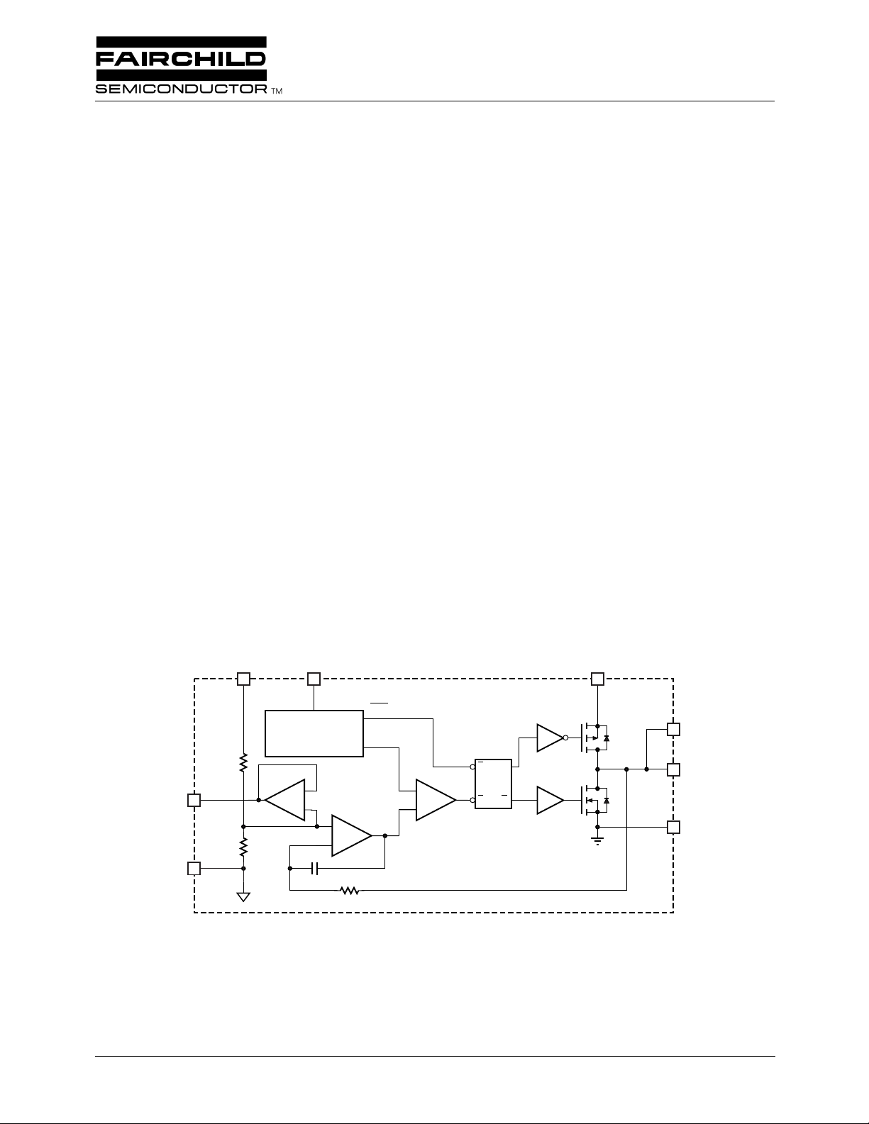
Block Diagram
General Description
The ML6553 switching regulator is designed to convert
voltage supplies ranging from 2.0V to 3.6V into a desired
output voltage or termination voltage for various applications. The ML6553 can be implemented to produce
regulated output voltages in two different modes. In the
default mode, the output is 50% of voltage applied to V
The switching regulator is capable of sourcing or sinking up
to 1A of current.
The ML6553, used in conjunction with series termination
resistors, provides an excellent voltage source for active
termination schemes of high speed transmission lines as
those seen in high speed memory buses and distributed backplane designs. The voltage output of the regulator can be
used as a termination voltage for other bus interface
standards such as SSTL, DDR, Rambus
™
, GTL+, VME,
LV-CMOS, LV-TTL, P-ECL, and CMOS.
CCQ
.
V
2
AGND
3
190kΩ
CCQ/2
1
V
CCQ
OSCILLATOR/
RAMP GENERATOR
BUFFER
190kΩ
4
AV
CC
CLK
RAMP
SRQ
–
+
V
INTEG
+
–
–
+
PWM
COMPARATOR
Q
5
PV
DD
V
L
Q1
Q2
6
V
L
7
DGND
8
REV. 1.0.2 3/21/01
Page 2
ML6553 PRODUCT SPECIFICATION
Pin Configuration
ML6553
8-Pin SOIC (S08)
DGND
V
V
CCQ/2
AGND
AV
CCQ
CC
1
2
3
4
TOP VIEW
8
V
7
L
V
6
L
PV
5
DD
Pin Description
Pin Name Function
1V
2V
CCQ
CCQ/2
3 AGND Analog signal ground
4AV
5PV
6V
7V
CC
DD
L
L
8 DGND Return for the internal power transistors.
Voltage supply for internal reference voltage divider
V
output is V
REF
CCQ/2
Voltage supply for the noise sensitive analog control section.
Voltage supply for the internal power transistors.
Output inductor connection
Output inductor connection
Absolute Maximum Ratings
Absolute maximum ratings are those values beyond which the device could be permanently damaged. Absolute maximum
ratings are stress ratings only and functional device operation is not implied.
Parameter Min. Max. Unit
V
IN
Voltage on Any Other Pin GND – 0.3 V
Peak Switch Current (I
Average Switch Current (I
)1A
PEAK
) 300 mA
AVG
5V
+ 0.3 V
IN
Junction Temperature 150 °C
Storage Temperature Range –65 150 °C
Lead Temperature (Soldering, 10 sec) 150 °C
Thermal Resistance ( θ
) 160 °C/W
JA
Output Current, Source or Sink 1 A
Operating Conditions
Temperature Range 0°C to 70°C
AV
, PV
CC
Operating Range 2.0V to 3.6V
DD
2
REV. 1.0.2 3/21/01
Page 3
PRODUCT SPECIFICATION ML6553
Electrical Characteristics
AV
= PV
CC
Symbol Parameter Conditions Min Typ Max Units
Switching Regulator
V
TT
V
CCQ/2
I
REF
Supply
I
Q
= 3.3V ±10%. Unless otherwise specified, T
DD
Output Voltage, V
TT
(See Figure 2) V
Output Voltage, V
Source Resistance from V
CCQ/2
L
I
OUT
REF
I
OUT
V
REF
Note 2 V
= Operating Temperature Range (Note 1)
A
= 0, V
= open V
= ±1A, V
= open V
= 2.3V 1.12 1.15 1.18 V
CCQ
= 2.5V 1.22 1.25 1.28 V
CCQ
V
= 2.7V 1.32 1.35 1.38 V
CCQ
= 2.3V 1.09 1.15 1.21 V
CCQ
= 2.5V 1.19 1.25 1.31 V
CCQ
= 2.7V 1.28 1.35 1.42 V
CCQ
V
= 2.3V 1.139 1.15 1.162 V
CCQ
V
= 2.5V 1.238 1.25 1.263 V
CCQ
V
= 2.7V 1.337 1.35 1.364 V
CCQ
20 m Ω
Switching Frequency 650 kHz
Output Load Current for V
CCQ/2
3mA
Pin
Quiescent Current I
= 0, no load I
OUT
VCCQ
I
AVCC
IPV
DD
10 µA
500 µA
4.5 mA
Notes:
1. Limits are guaranteed by 100% testing, sampling, or correlation with worst-case test conditions.
2. Specifications are taken from the application circuit in Figure 2 using the recommended component values.
REV. 1.0.2 3/21/01
3
Page 4

ML6553 PRODUCT SPECIFICATION
Functional Description
The ML6553 switching regulator is designed to sink and
source 1A load current and maintain a tight output voltage
regulation without the need for external feedback. Feedback
is accomplished internally by setting the average value of V
equal to V
ML6553 implements an open loop design that does not
require external loop compensation, providing a simplified
regulator design that can be used in cost sensitive applications.
Regulator Operation
Refer to the block diagram on the first page of this datasheet.
The oscillator/ramp block generates a 650kHz clock pulse
that is used to set the flip-flop. It also generates a 650kHz
ramp that the PWM comparator uses to reset the flip-flop.
When the flip-flop is set, the high side switch (Q1) is turned
through a high gain error amp. The
CCQ/2
on and the low side switch (Q2) is held off. In this state, the
voltage at V
is pulled up to PV
L
, which the error amp,
DD
integrates and inverts. The resulting output voltage of the
error amp will decline until it intersects the rising voltage of
the ramp. When this occurs the flip-flop is reset. In the reset
L
state, the high side switch is off, the low side switch is on
and V
is pulled to DGND. The flip-flop will remain in the
L
reset state until the next clock pulse. A timing diagram is
shown in Figure 1.
In the absence of a load, the duty cycle will be 50% if the
PV
and V
DD
will be half the voltage applied to V
are the same. The average voltage at V
CCQ
, and the net current
CCQ
change will be zero. If the ML6553 needs to source current,
the duty cycle will increase, resulting in more current being
supplied to the load. If the ML6553 needs to sink current, the
duty will decrease, resulting in current being pulled from the
load and returned back to the PV
DD
supply.
L
V
L
RAMP
V
INTEG
PWMCMP
CLK
Q
Figure 1. Timing Diagram
4
REV. 1.0.2 3/21/01
Page 5

PRODUCT SPECIFICATION ML6553
Design Consideration
Inductor Selection
The ML6553 requires the selection of an external inductor.
A value of 4.7µH is a good choice, but any value between
2.2µH and 10µH is acceptable. Choosing an inductance
value of less than 2.2µH will reduce the component’s footprint or the DC resistance, but the output voltage ripple will
increase. Conversely, inductance values greater than 10µH
will reduce the output ripple, but component size and output
regulation become issues.
It is important to use an inductor that is rated to handle 1.5A
peak currents without saturating. Also look for an inductor
with low winding resistance. An inductor with low winding
resistance leads to better regulation and higher output current
capability. A good rule of thumb is to use inductors with
20m Ω or less of winding resistance.
The final selection of the inductor will be based on trade-offs
between size, cost and performance. Make your selections
carefully. Inductor tolerance, core and copper loss will vary
with the type of inductor selected and should be evaluated
with the ML6553 under worst case conditions to determine
its suitability.
Input Capacitor
It is recommended to de-couple the PV
to 100µF capacitor. This provides the benefits of preventing
the input ripple from affecting the ML6553 control circuitry,
as well as improves the efficiency by reducing the I squared
R losses during the charge cycle of the inductor. Again, a low
ESR capacitor (such as tantalum) is recommended.
The AV
input should be de-coupled with at least a
CC
ceramic capacitor but a low pass RC filter is recommended if
the supply is particularly noisy. If a RC filter is used, the
series resistor value needs to low enough to prevent excessive voltage drops and high enough to provide effective
filtering. Resistor values on the order of 100 Ω are acceptable.
The V
if noise is present. The V
pin can also be bypassed with a ceramic capacitor
CCQ
pin can be de-coupled with a
CCQ
low pass RC filter if there is significant noise pickup on its
input. If a RC filter is used, resistor values on the order of
1,000 Ω are acceptable.
input with a 47µF
DD
Layout
Good layout practices will ensure the proper operation of the
ML6553. Some layout guidelines follow:
Suggested inductor for L1:
DC
Manufacturer Part No. Inductance
Resistance
Coiltronics UP3-4R7 4.7µH 0.011 Ω
Coiltronics (561) 241-7876
Output Capacitor
The output capacitor filters the pulses of current from the bus
terminator regulator as well as lowers the AC output impedance. For the best performance, one 330µF OS-CON decoupling capacitor is recommended.
Note that data transitions on the bus cause fast changes in
output current. These fast current changes cause high
frequency spikes to appear on the output. To minimize these
effects, choose an output capacitor with a combined ESR of
less than 50m Ω and use good layout practices to minimize
trace inductance from the output capacitors to the termination resistors. In addition, it is also recommended to bypass
the termination resistors with 0.01µF ceramic capacitors.
Suitable capacitors can be obtained from the following
vendors:
• Use adequate ground and power traces or planes.
• Keep the 47µF-100µF input capacitor as close to PV
DD
and DGND as possible.
• Use short trace lengths from the inductor to the V
pins
L
and from the inductor to the output capacitors.
• Use a separate trace from AGND to DGND, and use
DGND as the ground point for all the power components.
• Use additional bypass capacitors at each termination
resistor pack.
A typical application circuit schematic is shown in Figure 2,
and a sample layout is shown in Figure 3.
I
OUT MAX()
Where L
DCR
DESIRED
--------------------------------------------------------------------------------------------------------=
is the DC resistance of the output inductor, L1
OUTPUT
–()VTT×
OVA
L
0.020+
DCR
OVA
(1)
in Figure 2, and 0.020 is the source resistance of the output
V
. Both L
L
and 0.020 are in Ohms.
DCR
AVX (207) 282-5111 TPS Series
Sanyo (619) 661-6835 OS-CON Series
REV. 1.0.2 3/21/01
5
Page 6

ML6553 PRODUCT SPECIFICATION
Output Current Capability
The maximum current available at the output of the regulator
is related to the DC resistance of the inductor, the source
impedance of the ML6553, and the desired regulation. The
source impedance of the ML6553 can be estimated at 20m Ω
with an initial output voltage accuracy of ±1%. So the maximum output current can be estimated using:
DESIRED
-----------------------------------------------------------------------------------
I
OUT MAX()
≈ V
L
So, for an inductor with 11m Ω DC resistance, a termination
voltage of 1.25V, and a desired output voltage accuracy of
3%:
3% 1%–()1.25×
I
OUT MAX()
---------------------------------------------------------=
()100×
0.011 0.020+
V
CCQ
2.5V
V
CCQ/2
PV
DD
3.3V
GND
INITIAL
–()
OVA
DCR
C1
0.1µF
0.020+
R1
1kΩ
C2
0.1µF
OVA
0.806A=
R2
100Ω
0.1µF
×
C3
TT
(2)
1
2
3
4
V
CCQ
V
CCQ/2
AGND
AV
CC
This is enough current capability to terminate 50 bus lines,
assuming 16mA of drive current per line.
Since the feedback loop is closed internally on the ML6553
the total series resistance of the L/C output filter contributes
to increased deviation from no load to full load. The output
source impedance of the ML6553 is approximately 20m Ω .
A 1A load current yields 11mV (from L1) in output
deviation +20mV from the ML6553. Be sure to factor in the
component ESR values when constrained to a particular
maximum output deviation. Adequately bypass the V
output with SMD film capacitors to reduce transients
generated by stray lead inductance.
U1
ML6553
DGND
V
V
PV
DD
L
L
C4
100µF
8
7
6
5
L1
4.7µH
C5
330µF
OS-CON
C6
0.1µF
V
TT
TT
Figure 2. Application Schematic
Figure 3. ML6553 Board Layout
6
REV. 1.0.2 3/21/01
Page 7

ML6553 PRODUCT SPECIFICATION
Mechanical Dimensions Inches (Millimeters)
S08 8-Pin SOIC
0.189 - 0.199
(4.80 - 5.06)
8
0.017 - 0.027
(0.43 - 0.69)
(4 PLACES)
0.055 - 0.061
(1.40 - 1.55)
PIN 1 ID
1
0.050 BSC
(1.27 BSC)
0.012 - 0.020
(0.30 - 0.51)
SEATING PLANE
0.148 - 0.158
(3.76 - 4.01)
0.059 - 0.069
(1.49 - 1.75)
0.228 - 0.244
(5.79 - 6.20)
0.004 - 0.010
(0.10 - 0.26)
0º - 8º
0.015 - 0.035
(0.38 - 0.89)
0.006 - 0.010
(0.15 - 0.26)
Ordering Information
Part Number Temperature Range Package
ML6553CS-1 0°C to 70°C 8-Pin SOIC (S08)
DISCLAIMER
FAIRCHILD SEMICONDUCTOR RESERVES THE RIGHT TO MAKE CHANGES WITHOUT FURTHER NOTICE TO
ANY PRODUCTS HEREIN TO IMPROVE RELIABILITY, FUNCTION OR DESIGN. FAIRCHILD DOES NOT ASSUME
ANY LIABILITY ARISING OUT OF THE APPLICATION OR USE OF ANY PRODUCT OR CIRCUIT DESCRIBED HEREIN;
NEITHER DOES IT CONVEY ANY LICENSE UNDER ITS PATENT RIGHTS, NOR THE RIGHTS OF OTHERS.
LIFE SUPPORT POLICY
FAIRCHILD’S PRODUCTS ARE NOT AUTHORIZED FOR USE AS CRITICAL COMPONENTS IN LIFE SUPPORT DEVICES
OR SYSTEMS WITHOUT THE EXPRESS WRITTEN APPROVAL OF THE PRESIDENT OF FAIRCHILD SEMICONDUCTOR
CORPORATION. As used herein:
1. Life support devices or systems are devices or systems
which, (a) are intended for surgical implant into the body,
or (b) support or sustain life, and (c) whose failure to
perform when properly used in accordance with
2. A critical component in any component of a life support
device or system whose failure to perform can be
reasonably expected to cause the failure of the life support
device or system, or to affect its safety or effectiveness.
instructions for use provided in the labeling, can be
reasonably expected to result in a significant injury of the
user.
www.fairchildsemi.com
3/21/01 0.0m 003
2001 Fairchild Semiconductor Corporation
Stock#DS30001584
 Loading...