

Page 1
March 1997
ML6510*
Series Programmable Adaptive
Clock Manager (PACMan™)
GENERAL DESCRIPTION
The ML6510 (Super PACMan™) is a Programmable
Adaptive Clock Manager which offers an ideal solution for
managing high speed synchronous clock distribution in
next generation, high speed personal computer and
workstation system designs. It provides eight channels of
deskew buffers that adaptively compensate for clock skew
using only a single trace. The input clock can be either
TTL or PECL, selected by a bit in the control register.
Frequency multiplication or division is possible using the
M&N divider ratio, within the maximum frequency limit.
0.5X, 1X, 2X and 4X clocks can be easily realized.
The ML6510 is implemented using a low jitter PLL with
on-chip loop filter. The ML6510 deskew buffers adaptively
compensate for clock skew on PC boards. An internal
skew sense circuit is used to sense the skew caused by the
PCB trace and load delays. The sensing is done by
detecting a reflection from the load and the skew is
corrected adaptively via a unique phase control delay
circuit to provide low load-to-load skew, at the end of the
PCB traces. Additionally, the ML6510 supports PECL
reference clock outputs for use in the generation of clock
trees with minimal part-to-part skew. The chip configuration
can be programmed to generate the desired output
FEATURES
■ Input clocks can be either TTL or PECL with low
input to output clock phase error
■ 8 independent, automatically deskewed clock
outputs with up to 5ns of on-board deskew range
(10ns round trip)
■ Controlled edge rate TTL-compatible CMOS clock
outputs capable of driving 40Ω PCB traces
■ 10 to 80MHz (6510-80) or 10 to 130MHz (6510-130)
input and output clock frequency range
■ Less than 500ps skew between inputs at the
device loads
■ Small-swing reference clock outputs for minimizing
part-to-part skew
■ Frequency multiplication or division is possible using
the M&N divider ratio
■ Lock output indicates PLL and deskew buffer lock
■ Test mode operation allows PLL and deskew buffer
bypass for board debug
■ Supports industry standard processors like Pentium,™
Mips, SPARC,™ PowerPC,™ Alpha,™ etc.
frequency using the internal ROM or an external serial
EEPROM or a standard two-wire serial microprocessor
interface. *Some Packages Are Obsolete
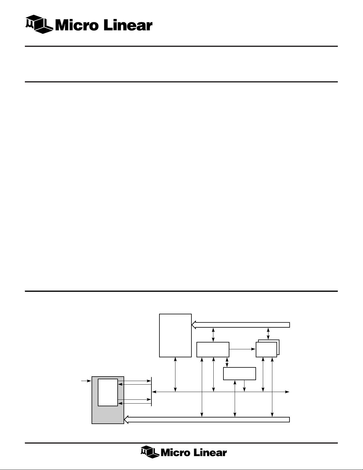
SYSTEM BLOCK DIAGRAM
CLOCK SUBSYSTEM
CLOCK IN
ML6510
LOCAL BUS
CPU
CACHE
CLK
•
8
•
•
CLOCK OUT TO
COMPONENTS
CONTROLLER
MEMORY BUS
CONTROLLER
MEMORY BUS
CACHE
RAM
1
Page 2
ML6510
BLOCK DIAGRAM
CLK
INL
CLK
INH
DESKEW BUFFER 0
RESET
LOCK
MD
R0MMSB
MCLK
MD
OUT
PHASE
DETECTOR
VOLTAGE
CONTROLLED
M
PLL
N
R
MAXIMUM
DELAY
IN
MAX DELAY
CONTROL LOGIC
PROGRAMMING AND
REF
CLOCK
RCLKH RCLKL
MAX DELAY
ZERO DELAY
ZERO DELAY
DELAY
DESKEW BUFFER 1
DESKEW BUFFER 7
SENSE
CIRCUIT
DRIVE
CIRCUIT
FB0
(from remote chip)
CLK0
(to remote chip)
FB1
CLK1
FB7
CLK7
PIN CONNECTION
CLK3
DVCC23
CLK2
DGND2
FB2
FB1
DGND1
CLK1
DVCC01
CLK0
DGND0
DGND3
FB3
AGND1
AVCC1
65432
7
8
9
10
11
12
13
14
15
16
17
18 19 20 21 22
44-LEAD PLCC (Q44)
IN
FB0
MD
OUT
MD
MCLK
FB4
DGND4
CLK4
DVCC45
CLK5
DGND5
FB5
140
43
44
ML6510
TOP VIEW
23 28
25
24
LOCK
RESET
AGND3
42
26
AVCC3
41
27
RCLKL
RCLKH
39
38
37
36
35
34
33
32
31
30
29
INH
CLK
FB6
DGND6
CLK6
DVCC67
CLK7
DGND7
FB7
ROMMSB
AVCC2
AGND2
CLK
INL
2
Page 3

PIN DESCRIPTION
PIN NUMBER NAME DESCRIPTION
32 ROMMSB MSB of the internal ROM address. Tie to GND if not used. See section on
ML6510
Programming the ML6510.
20 MD
19 MD
21 MCLK Programming pin. See section on Programming the ML6510.
22 RESET Reset all internal circuits. Asserted polarity is low.
23 LOCK Indicates when the PLL and deskew buffers have locked. Asserted polarity is
28 CLK
29 CLK
16,14,9,7, CLK[0–7] Clock outputs
44, 42, 37, 35
18,12,11,5, FB[0–7] Clock feedback inputs for the deskew buffers
2, 40, 39, 33
3,31 AVCC[1–3] Analog circuitry supply pins, separated from noisy digital supply pins to
25 provide isolation. All supplies are nominally +5V.
4, 30, 24 AGND[1–3] Analog circuitry ground pins
15 DVCC01 Digital supply pin for CLK0 and CLK1 output buffers. Nominally +5V.
8 DVCC23 Digital supply pin for CLK2 and CLK3 output buffers. Nominally +5V.
43 DVCC45 Digital supply pin for CLK4 and CLK5 output buffers. Nominally +5V.
OUT
IN
INH
INL
Programming pin. See section on Programming the ML6510.
Programming pin. See section on Programming the ML6510.
high.
Input clock pins. For TTL clock reference use CLK
shorted to the CLK
Input clock type is selected by the CS bit in the shift register.
pin. For PECL clock reference drive pins differentially.
INL
INH
pin
36 DVCC67 Digital supply pin for CLK6 and CLK7 output buffers. Nominally +5V.
17, 13, 10, 6, DGND[0–7] Digital ground pins for CLK [0–7] output buffers. Each clock output buffer has
1, 41, 38, 34 its own ground pin to avoid crosstalk and ground bounce problems.
26 RCLKL Differential reference clock output used to minimize
27 RCLKH part-to-part skew when building clock trees with other PACMan
integrated circuits.
3
Page 4
ML6510
ABSOLUTE MAXIMUM RATINGS
VCC Supply Voltage Range ............................ –0.3V to 6V
Input Voltage Range .................................... –0.3V to VCC
Output Current
Junction Temperature .............................................. 150°C
Storage Temperature................................ –65°C to 150°C
Thermal Resistance (θJA)....................................... 54°C/W
CLK[0–7] ........................................................ 70mA
All other outputs ............................................. 10mA
ELECTRICAL CHARACTERISTICS
The following specifications apply over the recommended operating conditions of DVCC = AVCC = 5V ± 5% and ambient
temperature between 0°C and 70°C. Loading conditions are specified individually (Note 1)
SYMBOL PARAMETER CONDITIONS MIN TYP MAX UNIT
SUPPLY
DVCCXX Supply Current for each pair f
of clock outputs
IAVCC1 Static supply current, AVCC1 pin 100 120 mA
IAVCC2 Static supply current, AVCC2 pin 35 40 mA
IAVCC3 Static supply current, AVCC3 pin 1 2 mA
LOW FREQUENCY INPUTS AND OUTPUTS (ROMMSB, MD
V
IH
V
IL
V
OH
High level input voltage DVCC – 0.5 V
Low level input voltage DGND + 0.5 V
High level output voltage, IOH = –100 µA DVCC – 0.5 V
MCLK and MDIN
= 0 50 µA
CLKX
CL= 20pF, ZO = 50Ω 40 60 mA
f
= 80MHz
OUT
, MDIN, MCLK, RESET, LOCK)
OUT
V
OL
Low level output voltage, IOL = +200 µA DGND + 0.5 V
MCLK and MDIN
V
OH
High level output voltage, IOH = –100 µA 2.4 V
LOCK output IOH = –10 µA DVCC – 0.5 V
V
OL
Low level output voltage, IOL = +1 mA 0.4 V
LOCK output
I
IN
C
IN
Static input current 10 µA
Input capacitance 5 pF
HIGH FREQUENCY INPUTS AND OUTPUTS (CLK
V
IH
V
IL
V
ICM
High level input voltage CS = 0 (TTL Input Clock) 2.0 V
Low level input voltage CS = 0 (TTL Input Clock) 0.8 V
Common mode input voltage CS = 1 (PECL Input Clock) 2.0 AVCC – 0.4 V
range for PECL reference clocks
I
IH
I
IL
V
OH
V
OL
High level input current VIH = 2.4V 100 µA
Low level input current VIL = 0.4V –400 µA
High level output voltage IOH = –60mA 2.4 V
Low level output voltage IOL = +60mA 0.4 V
INH
, CLK
, FB[0-7], CLK[0-7])
INL
CS = 1 (PECL Input Clock) AVCC – 1.165 AVCC – 0.88 V
CS = 1 (PECL Input Clock) AVCC – 1.810 AVCC – 1.475 V
4
Page 5
ML6510
ELECTRICAL CHARACTERISTICS (Continued)
SYMBOL PARAMETER CONDITIONS MIN TYP MAX UNIT
AC CHARACTERISTICS rise time, fall time and duty cycle are measured for a generic load; (see Load Conditions section).
t
R
t
F
f
IN
f
OUT
f
VCO
Rise time, LOAD [0-7] output 0.8 → 2.0V, 80MHz 150 1500 ps
Fall time, LOAD [0-7] output 2.0 → 0.8V, 80MHz 150 1500 ps
Input frequency, CLKIN pin 10 80 MHz
Output frequency , CLK [0-7] ML6510-80 10 80 MHz
output
ML6510-130 (Note 2) 10 130 MHz
PLL VCO operating frequency 80 160 MHz
DC Output duty cycle Measured at device load, at 1.5V 40 60 %
t
JITTER
Output jitter Cycle-to-cycle 75 ps
Peak-to-peak 150 ps
t
LOCK
PLL and deskew lock time After programming is complete 11 ms
SKEW CHARACTERISTICS All skew measurements are made at the load, at 1.5V threshold each output load can vary independently
within the specified range for a generic load (see Load Conditions section).
t
SKEWR
Output to output rising 500 ps
edge skew, all clocks
t
SKEWF
Output to output Output clock frequency ≥ 50MHz 1.5 ns
falling edge skew
t
SKEWIO
CLKIN input to any N = M = 0 600 ps
LOAD [0-7] output
rising edge skew N ≥ 2, M ≥ 2 1.25 ns
t
RANGE
t
SKEWB
Round trip delay CLKX to FBX Output frequency < 50MHz 0 10 ns
pin; output CLK period = t
CLK
Output frequency ≥ 50MHz 0 t
CLK
/2
Output-to-output rising Providing first (see LOAD 250 ps
edge skew, between matched conditions) order matching
loads order matching between outputs
PART-TO-PART SKEW CHARACTERISTICS Skew measured at the loads, at 1.5V threshold. Reference clock output pins drive clock
input pins of another ML6510.
t
PP1
Total load-to-load skew between Slave chip CS = 1, CM = 1 and 1 ns
multiple chips interfaced with N = 0, M = 0; RCLK outputs to
reference clock pins. CLKIN inputs distance less than 2"
t
PP2
Total load-to-load skew between Slave chip CS = 1, CM = 1 and 1 ns
multiple chips interfaced with N ≥ 2, M ≥ 2; RCLK outputs to
reference clock pins. CLKIN inputs distance less than 2"
PROGRAMMING TIMING CHARACTERISTICS
tRESET RESET assertion pulse 50 ns
width
t
A1
t
A2
t
A3
AUX mode MCLK high time 2000 ns
AUX mode MCLK low time 2000 ns
AUX mode MD
data 10 ns
OUT
hold time
t
A4
AUX mode MD
data 10 ns
OUT
setup time
t
A5
AUX mode MCLK period 5000 ns
5
Page 6
ML6510
ELECTRICAL CHARACTERISTICS (Continued)
SYMBOL PARAMETER CONDITIONS MIN TYP MAX UNIT
PROGRAMMING TIMING CHARACTERISTICS (continued)
t
M1
t
M2
t
M3
t
M4
MAIN mode MCLK high time 900 ns
MAIN mode MCLK low time 900 ns
MAIN mode MCLK period 1800 ns
MAIN mode 900 ns
MCLK to MD
OUT
valid
(EEPROM read time)
Note 1: Limits are guaranteed by 100% testing, sampling or correlation with worst case test conditions.
Note 2: If ML6510-130 is used in a master-slave mode, the maximum operating frequency is 120MHz.
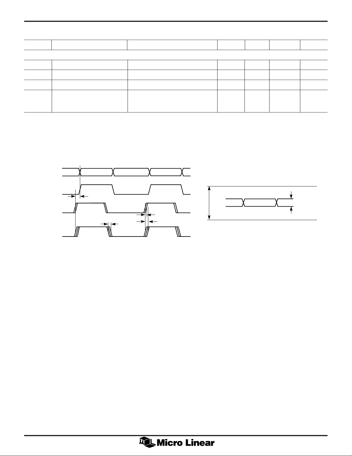
ML6510 configured with bit CM = 0:
PECL INPUT CLOCKS
OR
TTL INPUT CLOCK
LOAD [0-7]
1st Order Match
OR
t
SKEWIO
t
SKEWF
t
SKEWB
t
SKEWR
CLK
CLK
V
ICM
AVCC – 0.4V
INH
INL
2.0 V
LOAD [0-7] with
no 1st order match
Note: All skew is measured at the device load input pin, NOT at the ML6510 clock output pin. Skew is always a positive number, regardless of which edge is leading and
which is trailing.
6
Page 7

AC/SKEW CHARACTERISTICS LOAD CONDITIONS
ML6510
ML6510-80
GENERIC
ML6510-80
FIRST-ORDER
MATCHED LOADS
LOAD
FBX
CLKX
FBX
CLKX
FBY
CLKY
PCB trace impedance
Z0 = 50Ω
R1
One way trip delay < t
PCB trace impedance
Z0 = 50Ω
R1
Length L
PCB trace impedance
Z0 = 50Ω
R1
Length L
One way trip delay < t
RANGE
X
Y
RANGE
LOAD
Lumped
CL ≤ 20pF
/2
LOAD
Lumped
C
LX
|CLX – CLY| < 5pF
|L
– LY| < 4"
X
Z
= Z
OX
OY
LOAD
Lumped
C
LY
/2
≤ 20pF
≤ 20pF
ML6510-130
GENERIC
ML6510-130
FIRST-ORDER
MATCHED LOADS
LOAD
FBX
CLKX
FBX
CLKX
FBY
CLKY
PCB trace impedance
Z
= 50Ω
0
R2
R3
One way trip delay < t
PCB trace impedance
Z0 = 50Ω
R2
R3
PCB trace impedance
Z0 = 50Ω
R2
R3
One way trip delay < t
Length L
Length L
X
Y
RANGE
LOAD
Lumped
CL ≤ 20pF
/2
RANGE
LOAD
Lumped
C
LX
|CLX – CLY| < 5pF
|L
– LY| < 4"
X
Z
= Z
OX
OY
LOAD
Lumped
C
LY
/2
≤ 20pF
≤ 20pF
ML6510
RCLKH RCLKL
CLK
CLK
INH
ML6510
SLAVE CHIP
(CM=1, CS=1)
INL
DISTANCE <2"
LOAD[0-7]
LOAD[8-15]
LOAD[0-7]
LOAD[8-15]
t
SKEWR
t
SKEWR
t
pp1
or t
(or t
(or t
pp2
SKEWB
SKEWB
)
)
7
Page 8

ML6510
WRITE
SIGNAL
CLOCK AT
REMOTE CHIP
DATA AT
REMOTE CHIP
WRITE
SIGNAL
CLOCK AT
REMOTE CHIP
DATA AT
REMOTE CHIP
DATA
DATA
t
S
t
H
FUNCTIONAL DESCRIPTION
Micro Linear’s ML6510 is the first clock chip to use a
feedback mechanism to adaptively (on a real time basis),
eliminate clock skew in high speed personal computer
and workstation system designs. Figure 1 shows a basic
configuration of the ML6510 in a system. The skew
problem results due to the delaying of clock signals in the
system, as shown in Figure 2. Clock skew results from
variation in factors like trace length, PCB trace
characteristics, load capacitance, parasitic capacitance,
temperature and supply variations, etc. Figure 2 shows a
representation of the clock skew problem from a timing
perspective. It shows a worst case example where the
clock signal is delayed so much that its rising edge
completely misses the data it is intended to strobe.
Using a clock deskew mechanism, this problem can be
eliminated and the strobe with the appropriate setup and
hold times with respect to the data bus can be generated.
The ML6510 has eight deskew buffers, each with its own
independent the reflection and error correction circuit.
The deskew buffer eliminates skew by using the reflection
from a remote chip to measure the clock error and then
corrects it by generating the appropriate skew to the clock
output to compensate.
Eight individually deskewed copies of the clock are
provided by the ML6510.
The deskew buffers compensate internally for board-level
skew caused by the PCB trace length variations and
device load variations. This is accomplished by sensing
the round trip delay via a reflected signal, and then
delaying or advancing the clock edge so that all 8 output
clocks arrive at their loads in phase. Each of the eight
clock lines can have any length PCB trace (up to 5ns each
way or 1/4th of the output clock period, whichever is
smaller) and the device loads can vary from line to line.
The ML6510 will automatically compensate for these
variations, keeping the device load clocks in phase.
Although ML6510 will compensate for skew caused by
loading, excessive capacitive loading can cause rise/fall
time degradation at the load. Cascading one ML6510 to
another ML6510 should be done using the PECL reference
clock outputs, to minimize part-to-part skew.
CLOCK REGENERATION
The programmable adaptive clock deskew can function in
a clock regeneration mode to assist in building clock trees
or to expand the number of deskewed clock lines. In this
mode, it has the ability to do clock multiplication or
division as well, while maintaining low skew between
Figure 1. Basic System Configuration Using the ML6510.
CLOCK
GENERATOR
CLOCK IN
MICRO LINEAR
ML6510
CLOCK CHIP
CPU
CLOCK #0
FEEDBACK #0
CLOCK #1
FEEDBACK #1
CLOCK #7
FEEDBACK #7
DATA
REMOTE
CHIP
Figure 2. The Skew Problem.
8
Page 9

CLK
CLK
INH
INL
ECL INPUT BUFFER
TTL TO ECL
1
0
CS BIT
÷(M + 1)
[÷1 TO 64]
PHASE
DETECTOR
LOOP
FILTER
VCO
80-160 MHz
MAXIMUM
R
÷2
DELAY
ML6510
RCLKH
RCLKL
÷(N + 1)
[÷1 TO ÷128]
Figure 3. ML6510 Clock Generation Block Diagram.
input clock and output clocks. It can thus generate a 2x or
4x or 0.5x frequency multiplication or division from input
to output (e.g. 33 MHz input, 66 MHz output or 66 MHz
input, 33 MHz output, etc.). It also can generate a 1x
frequency output. The VCO frequency is defined by:
R
+
×
12
M
+
1
ff
=×
VCO REF
N
()
()
and the output frequency is still given by:
f
= f
OUT
R1 R0 INPUT/OUTPUT RANGE
0 0 80-130 MHz
0 1 40–80 MHz
1 0 20–40 MHz
1 1 10–20 MHz
Note: R implies R1, R0; for -80 version, Not valid: Defaults to R = 01
VCO
/2
R
The VCO still must remain in the range 80–160 MHz, and
the minimum phase detector input frequency is 625kHz =
(80 MHz/128). Thus the product of (N + 1) and 2R should
be limited to 128:
(N + 1) x 2
R
≤ 128 to make sure that the
phase detector inputs
remain above the minimum
frequency.
1
0
1
CM BIT
0
SYS_CLK
TO DESKEW BUFFERS
TEST
Example: Generating a 2x clock input frequency = 33 MHz
Set R = 01 (output range 40 – 80 MHz), N = 5 (0000101),
M = 2 (000010), M/S = 0
R
×
+
12
+
M
1
MHz MHz
=×
33
×
62
3
/2R = 132 MHz/21 = 66 MHz
1
132
=
ff
=×
VCO REF
f
= f
OUT
N
()
()
VCO
Example: Generating a 1x clock Input frequency = 66 MHz
Set R = 01 (output range 40–80 MHz), set M = 0
(000000), N = 0 (0000000), M/S = 0
1
12
×
=66
f MHz MHz
f
OUT
=×
VCO
= f
/2R = 132 MHz/21 = 66 MHz
VCO
1
132
For doing frequency multiplication and division, keep
M ≥ 2 and N ≥ 2 for the lowest skew between input
clock and output clock. Several configurations for doing
frequency multiplication and division are included in the
8 configurations stored in the on-chip ROM (see
PROGRAMMING the ML6510).
9
Page 10

ML6510
ADAPTIVE DESKEW BUFFERS
Each copy of the clock is driven by an adaptive deskew
buffer. The deskew buffer compensates for skew time
automatically in accordance to the flight time delay it
senses from the reflection on the transmission line.
Figure 4 shows the simplified functional block diagram of
the deskew circuit. The phase of the sense signal and the
driver signal is presented to a three-input phase
comparator and compared with the reference signal. The
phase comparator then controls the voltage controlled
delay in the output drive line to match the delay of the
fixed reference delay line. Therefore, the sum of the delay
of the driver circuit, PCB trace delay, rise time delay at the
load and the adjustable delay will always equal the fixed
maximum delay.
The sense circuit has an internal level detect such that any
skew caused by loading is also accounted for. Since the
delay of the circuit is matched for the entire loop, the
phase of all the drivers are in close alignment at the inputs
of the load.
FIXED
CLOCK IN
MAX
DELAY
LOAD CONDITIONS
The ML6510 has been designed to drive the wide range of
load conditions that are encountered in a high frequency
system. The eight output clock loads can each vary within a
range of trace length and lumped capacitive load, and the
ML6510 will maintain the low skew characteristics specified
in Electrical Characteristics. The clock skew can be further
minimized by providing some first-order matching
between any two loads that require particularly wellmatched clocks.
The ML6510-80 produces a 5V swing at the load and
requires a single external termination resistor for each
output. The ML6510-130 produces a 3V swing at the load
and requires two external termination resistors for each
output. The FB input pin is connected to the other side of
the termination resistor R1 or R2, with a short connection.
Termination resistor valves should be chosen as follows:
RZ R Z R Z121533
==×=×.
000
TRACE RESISTOR
IMPEDANCE VALUES
Z0 R1 R2 R3
40Ω 40 60 120
50Ω 50 75 150
63Ω 63 95 189
PHASE
DETECTOR
VOLTAGE
CONTROLLED
DELAY
SENSE
DRIVE
Figure 4. Deskew Circuit Block Diagram.
LOAD
10
Page 11

ML6510
CHIP
VCC
RESET
LOCK
t
RESET
t
LOCK
t
LOCK
PROGRAM IN THE
CONFIGURATION
PROGRAM IN THE
CONFIGURATION
0
5V
ML6510-80
GENERIC
ML6510-80
FIRST-ORDER
MATCHED LOADS
LOAD
FBX
CLKX
FBX
CLKX
FBY
CLKY
PCB trace impedance
Z0 = 40Ω to 65Ω
R1
One way trip delay < t
PCB trace impedance
Z0 = 40Ω to 65Ω
R1
Length L
PCB trace impedance
Z0 = 40Ω to 65Ω
R1
Length L
One way trip delay < t
RANGE
X
Y
RANGE
LOAD
Lumped
CL ≤ 20pF
/2
LOAD
Lumped
C
LX
|CLX – CLY| < 5pF
|L
– LY| < 4"
X
Z
= Z
OX
OY
LOAD
Lumped
C
LY
/2
≤ 20pF
≤ 20pF
ML6510-130
GENERIC
ML6510-130
FIRST-ORDER
MATCHED LOADS
LOAD
FBX
CLKX
FBX
CLKX
FBY
CLKY
PCB trace impedance
Z0 = 40Ω to 65Ω
R2
R3
One way trip delay < t
PCB trace impedance
Z0 = 40Ω to 65Ω
R2
R3
PCB trace impedance
Z0 = 40Ω to 65Ω
R2
R3
One way trip delay < t
Length L
Length L
X
Y
RANGE
LOAD
Lumped
CL ≤ 20pF
/2
RANGE
LOAD
Lumped
C
LX
|CLX – CLY| < 5pF
|L
– LY| < 4"
X
Z
= Z
OX
OY
LOAD
Lumped
C
LY
/2
≤ 20pF
≤ 20pF
EXTERNAL INPUT CLOCKS
The external input clock to the ML6510 can be either a
differential Pseudo-ECL clock or a single-ended TTL clock.
This is selected using the CS bit in the serial shift register.
For the single-ended TTL clock tie the CLK
and CLK
INH
INL
pins together. The ML6510 ensures that there is a welldefined phase difference between the input and output
clocks.
RESET AND LOCK
When RESET is de-asserted, the internal programming
logic will become active, loading in the configuration bits
(see Programming the ML6510). Once the configuration is
loaded, the PLL will lock onto the reference signal, and
then the deskew blocks will adapt to the load conditions.
When all eight output clocks are stable and deskewed,
LOCK will be asserted. The asserted polarity of lock is
high. Thus, LOCK can be used to indicate that the system
is ready, or it can be used to drive the RESET input of
another PACMan in a clock tree.
RESET may be reasserted at any time to reset the chip
operations. Following a RESET assertion of valid pulse
width (see Programming Electrical Characteristics), the
ML6510 must again be loaded with a configuration, then
it will re-lock and reassert lock when all eight clock
outputs are stable and deskewed.
11
Page 12

ML6510
PROGRAMMING THE ML6510
The configuration of the ML6510 is programmed by
loading 18 (ML6510-80) or 19 (ML6510-130) bits into the
configuration shift register. To load these bits, the user has
3 options: MAIN, AUX or ROM modes. Which mode is
used is determined by the logic level on the MDIN pin
when RESET is deasserted. If MDIN is tied high, the
ML6510 will assume AUX mode; if its tied low, ROM
mode. If MDIN is high-impedance (i.e. tied to the input of
an EEPROM), it will assume MAIN mode.
1. MAIN Mode
In this mode, the ML6510 will read the configuration bits
from an external serial EEPROM, such as the 93C46, using
the industry standard 3-wire serial I/O protocol. The serial
EEPROM should be a 1K organized in 64 x 16 bits and the
PACMan will read the configuration bits out of the two least
significant 16-bit words. To use this mode, simply connect
the EEPROM serial data input pin to MDIN (ML6510 pin 19),
the EEPROM serial data output pin to MD
20), and the EEPROM serial data clock pin to MCLK
(ML6510 pin 21) and CS pin for the EEPROM should be tied
to the RESET signal. After power up, when RESET is
deasserted, the ML6510 will automatically generate the
address and clock to read out the configuration bits. Refer
MAIN Mode waveform in Figure 5.
1K SERIAL
EEPROM
(64 X 16 BIT)
CLOCK
OPCODES
ADDRESS
DATA
RESET
CS
CLK
DATA IN
DATA OUT
MAIN Mode Configuration.
(ML6510 pin
OUT
ML6510
ROMMSB
MCLK
MD
IN
MD
OUT
RESET
2. AUX Mode
When MDIN is tied to VCC, programming the ML6510
will occur via the AUX Mode. This mode shifts the
configuration bits into the shift register directly from the
MD
pin. The first 18 (ML6510-80) or 19 (ML6510-
OUT
130) clock rising edges provided externally on the MCLK
pin after RESET is deasserted will be used to load the shift
register data, which should be provided on the MD
OUT
pin. See figure 6.
µ PROCESSOR
CLOCK
VCC
DATA
ML6510
ROMMSB
MCLK
MD
IN
MD
OUT
AUX Mode Configuration.
3. ROM Mode
When MDIN is tied to GND, programming the ML6510
will occur via the ROM Mode. This mode reads the
configuration bits directly from an on chip ROM. The
selection of one of the eight preset configuration codes is
accomplished by means of the pins ROMMSB, MCLK and
MD
as shown in Tables 1 and 2. The TEST mode
OUT
configuration (code 7) is enabled when the TEST bit is set.
In this mode the PLL is bypassed for low frequency testing.
Codes 0-2 are used when the ML6510 clock inputs are
driven from another PACMan’s reference clock outputs.
Code 3 is used when zero phase error is desired between
input and load clocks.
ML6510
ROM
ADDRESS
BITS
ROMMSB
MCLK
MD
OUT
MDIN
ROM
8 X 19 BIT
TO SHIFT REGISTER
SERIAL DATA IN
(Driven by
(Driven by
(Driven by
12
MCLK
ML6510)
MD
ML6510)
MD
OUT
EEPROM)
t
M1
01 02 03 04 05 06 07 08 09 10 11 12 • • • 25
IN
SB1OP1
1
t
M2
A50A40A30A20A10A0
OP0
0
t
M3
0
t
M4
ROM Mode Configuration.
D13 D15 D14
16 bits data at adddress 0
Figure 5. MAIN Mode Waveforms.
26 2713
• • •D15 D14
D0
2 bits at address 1
(3 bits for ML6510-130)
(28)
(D13)
Page 13

ML6510
TABLE 1: ML6510-80 ROM CODES
SELECTION BITS INPUT OUTPUT CONFIGURATION CODE
FREQ FREQ
CODE DESCRIPTION ROMMSB MCLK MD
0 PECL Input Clock, 1x mode 0 0 0 40-80 40-80 1 1 01 0 0 0
1 PECL Input Clock, 0.5x mode 0 0 1 40-80 20-40 1 1 10 5 2 0
2 PECL Input Clock, 2x mode 0 1 0 20-40 40-80 1 1 01 2 5 0
3 PECL Input Clock, 1x mode 0 1 1 40-80 40-80 1 0 01 0 0 0
4 TTL Input Clock, 1x mode 1 0 0 40-80 40-80 0 0 01 0 0 0
5 TTL Input Clock, 0.5x mode 1 0 1 40-80 20-40 0 0 10 5 2 0
6 TTL Input Clock, 2x mode 1 1 0 20-40 40-80 0 0 01 2 5 0
7 TEST mode, TTL Input clock 1 1 1 0-50 0-50 0 — — — — 1
TABLE 2: ML6510-130 ROM CODES
SELECTION BITS INPUT OUTPUT CONFIGURATION CODE
CODE DESCRIPTION ROMMSB MCLK MD
0 PECL Input Clock, 1x mode 0 0 0 80-130 80-130 1 1 00 0 0 0 0
1 PECL Input Clock, 0.5x mode 0 0 1 80-160 40-80 1 1 01 5 2 0 0
2 PECL Input Clock, 2x mode 0 1 0 40-65 80-130 1 1 00 2 5 0 0
3 PECL Input Clock, 1x mode 0 1 1 80-130 80-130 1 0 00 0 0 0 0
4 TTL Input Clock, 1x mode 1 0 0 80-130 80-130 0 0 00 0 0 0 0
5 TTL Input Clock, 0.5x mode 1 0 1 80-130 40-65 0 0 01 5 2 0 0
6 TTL Input Clock, 2x mode 1 1 0 40-65 80-130 0 0 00 2 5 0 0
7 TEST mode, TTL Input clock 1 1 1 0-50 0-50 0 — — — — — 1
(MHz) (MHz) CS CM R1, R0 M N TEST
OUT
FREQ FREQ
(MHz) (MHz) CS CM R1, R0 M N DDSK TEST
OUT
MCLK
(Input to ML6510)
MD
OUT
(Input to ML6510)
t
A2
M5 N0
t
A3
t
A1
t
A4
M4
t
A5
Figure 6. AUX Mode Waveform.
180201
13
Page 14

ML6510
REGISTER DEFINITIONS
REGISTER SIZE FUNCTION
N 7 bit This register is used to define the ratio for the desired frequency of the primary clock.
R 2 bit This register defines the frequency of the primary clocks, CLK [0-7].
CM 1 bit Set CM = 1 when the PECL input reference clock is from another 6510 reference clock output. Set
CM = 0 if the clock reference is TTL or PECL from an external source and minimum phase error
between input and output is desired.
CS 1 bit CS = 0 selects TTL input clock, CS = 1 selects PECL input clock.
TEST 1 bit When set to 1, the PLL is bypassed for low frequency testing.
M 6 bit This register is used to define the ratio for the desired frequency of the primary clock.
DDSK 1 bit When DDSK is set to 1, deskew is disabled. The chip will provide low skew clocks at the chip output
pins, but trace length variations will not be compensated. When DDSK is set to 0, normal deskew will
provide low skew clocks at the loads. This bit is only for ML6510-130.
ML6510-80 SHIFT REGISTER CHAIN
CM
CS M0
TEST M1 M2 M3 M4 M5
LSB
MSB
SERIAL DATA IN
(from EEPROM,
or µProcessor,
or internal ROM)
N1 N2 N3 N4 N5 N6
N0
LSB
MSBR0LSBR1MSB
ML6510-130 SHIFT REGISTER CHAIN
N1 N2 N3 N4 N5 N6
N0
SERIAL DATA IN
(from EEPROM,
or µProcessor,
or internal ROM)
LSB
MSBR0LSBR1MSB
DDSK
CM
CS M0
TEST M1 M2 M3 M4 M5
LSB
MSB
14
Page 15

APPLICATIONS
ML6510
ML6510
(SLAVE MODE)
ML6510
ZERO SKEW CLOCK GENERATION
The most advantageous feature of using PACMan is its
ability to deliver multiple copies of the clock to the load
with very low skew. Because of its unique ability in
deskewing, trace length and load consideration are no
longer critical in board design.
Because of the unique deskewing scheme, neither the
trace length nor the device loads need to be equal. This is
true for loads, <20pF. Higher loads can be driven if they
are placed close to the clock chip, to guarantee signal
integrity.
CLOCK
DRIVER
tO–tS1
1
t
tO–tS2
t
O–tS
t
2
S
3
t
3
S
ONE
DEVICE
LOAD
0t
t
S
TWO
DEVICE
LOAD
S
0t
S
THREE
DEVICE
LOAD
0
S
LOW SKEW CLOCK DISTRIBUTION
Clock distribution design is usually not a trivial task,
especially when multiple clock chips are needed. By
using closely grouped PACMans, 16 or more clock lines
can be created with low part-to-part skew. Additional
groups of clocks can be clustered and driven from
deskewed clock lines, to minimize the number of longdistance clock lines.
ML6510
ML6510
CLK0
CLK1
CLK2
• • • • • •
CLK0
CLK1
CLK2
ML6510
TO REMOTE GROUP
OF CLUSTERED LOADS
CLK0
CLK1
CLK2
CLK3
• • •
BOARD TO BOARD SYNCHRONIZATION
Distribution of the synchronous clock could present
significant difficulty at high frequency. With the system
clock generated by the ML6510, a zero skew clock
delivery to a backplane is now possible. By using the
ML6510 slave chip or the ML6510 in slave mode at the
receiver end, a near zero delay clock link can be
accomplished between the mother board and the satellite
boards.
Because the PACMan has frequency doubling capability, a
lower frequency signal can be used to route across a back
plane.
EXAMPLE CONFIGURATION
Shown in Figure 7 is an example configuration using
two ML6510-80 chips in tandem to generate eight 66
MHz clocks and eight 33MHz low-skew clocks from a
66MHz input reference. This requires only the termination
resistors. Configurations are loaded from the internal
ROM. PCB traces 0 to 15 are each 50Ω impedance and
the load capacitances CL0-C
are 0 to 20pF each. No
L15
trace length matching is required among separate clock
outputs. All traces are shown with a series termination at
the output. If ML6510-130’s are used in a master slave
mode the maximum operating frequency will be 120MHz.
t
pp2
LOAD[0-7]
LOAD[8-15]
33 MHz
t
SKEWR
t
SKEWR
(or t
(or t
SKEWB
SKEWB
)
)
15
Page 16

ML6510
SYSTEM RESET LOW
VCC
66MHz
TTL REFERENCE
RESET
ROMMSB
MCLK
MD
IN
MD
OUT
CLK
INH
CLK
INL
LOCK
ML6510-80
TTL 1X
MODE
RCLKH RCLKL
66MHz
CLK
INH
CLK
INL
CLK0
FB0
CLK1
FB1
CLK7
FB7
CLK0
50
50
50
50
PCB TRACE 0
PCB TRACE 1
PCB TRACE 7
PCB TRACE 8
LOAD7
LOAD0
66 MHz
C
L7
LOAD8
66 MHz
C
L0
LOAD1
33 MHz
66 MHz
C
L1
RESET
ROMMSB
MCLK
MD
VCC
MD
ALL_CLOCK_READY
IN
OUT
LOCK
ML6510-80
PECL 0.5X
MODE
FB0
CLK1
FB1
CLK7
FB7
50
50
PCB TRACE 9
PCB TRACE 15
LOAD15
33 MHz
C
L15
C
L8
LOAD9
33 MHz
C
L9
16
Figure 7. Example use of two ML6510-80 to generate multiple frequency clocks.
First ML6510-80 generates eight 66MHz clocks while second ML6510-80 takes 66MHz
small-swing reference from the first chip and generates eight 33MHz clocks.
Page 17

ML6510
PHYSICAL DIMENSIONS inches (millimeters)
0.685 - 0.695
(17.40 - 17.65)
0.650 - 0.656
(16.51 - 16.66)
1
Package: Q44
44-Pin PLCC
0.042 - 0.056
(1.07 - 1.42)
0.025 - 0.045
(0.63 - 1.14)
(RADIUS)
0.042 - 0.048
(1.07 - 1.22)
12
0.050 BSC
(1.27 BSC)
0.013 - 0.021
(0.33 - 0.53)
PIN 1 ID
23
0.026 - 0.032
(0.66 - 0.81)
34
0.165 - 0.180
(4.06 - 4.57)
SEATING PLANE
0.650 - 0.656
(16.51 - 16.66)
0.148 - 0.156
(3.76 - 3.96)
0.685 - 0.695
(17.40 - 17.65)
0.009 - 0.011
(0.23 - 0.28)
0.100 - 0.112
(2.54 - 2.84)
0.500 BSC
(12.70 BSC)
0.590 - 0.630
(14.99 - 16.00)
18
Page 18

ML6510
ORDERING INFORMATION
PART NUMBER TEMPERATURE RANGE PACKAGE
ML6510CQ-80 0°C to 70°C 44-pin PLCC (Q44)
ML6510CQ-1300°C to 70°C44-pin PLCC (Q44) (Obsolete)
© Micro Linear 1997 is a registered trademark of Micro Linear Corporation
Products described in this document may be covered by one or more of the following patents, U.S.: 4,897,611; 4,964,026; 5,027,116; 5,281,862; 5,283,483; 5,418,502; 5,508,570; 5,510,727; 5,523,940;
5,546,017; 5,559,470; 5,565,761; 5,592,128; 5,594,376; Japan: 2598946. Other patents are pending.
Micro Linear reserves the right to make changes to any product herein to improve reliability, function or design.
Micro Linear does not assume any liability arising out of the application or use of any product described herein,
neither does it convey any license under its patent right nor the rights of others. The circuits contained in this
data sheet are offered as possible applications only. Micro Linear makes no warranties or representations as to
whether the illustrated circuits infringe any intellectual property rights of others, and will accept no responsibility
or liability for use of any application herein. The customer is urged to consult with appropriate legal counsel
before deciding on a particular application.
18
2092 Concourse Drive
San Jose, CA 95131
Tel: 408/433-5200
Fax: 408/432-0295
DS6510-01
 Loading...