

Page 1
February 1997
ML6509*
Active SCSI Terminator
GENERAL DESCRIPTION
The ML6509 BiCMOS SCSI terminator provides active
termination in a SCSI system with single ended drivers and
receivers, in full compliance with the SCSI-1, SCSI-2 and
SCSI-3 recommendations. It provides a 2.85V reference
through an internal 1V dropout linear regulator. Active
SCSI termination helps the system designer to effectively
control analog transmission line effects like ringing, noise,
crosstalk, ground bounce, etc. In addition it provides
greater immunity to voltage drops on the TERMPWR line
of the SCSI bus. The desired V-I characteristics for signal
negation requires that the terminator source 0–24mA
while maintaining 2.85V and for signal assertion
preferably follow a linear slope of 110W. The ML6509
attempts to provide a V-I characteristic optimized to
minimize the transmission line effects during both signal
assertion and negation, using a MOSFET based
architecture. The desired V-I characteristic is achieved by
trimming one resistor in the control block. It provides
negative clamping for signal assertion transients and
current sink capability, to handle active negation driver
overshoots above 2.85V, which is currently accomplished
with external components in SCSI subsystems today. It
provides a disconnect mode, where the terminator is
completely disconnected from the SCSI
bus and the output capacitance is < 5pF, typically.
FEATURES
■ Fully monolithic IC solution providing active
termination for 9 lines of the SCSI bus
■ Low dropout voltage (1V) linear regulator, trimmed for
accurate termination current, with 300mA current
source capability
■ Output capacitance typically <5pF
■ Disconnect mode — logic pin to disconnect terminator
from the SCSI bus, <100µA
■ Lowpower mode — for power conscious, portable
system & peripheral applications, using less than 6"
cables. (Equivalent to a 1mA current drive with a
2.5kW termination)
■ Current sinking — can sink current >10mA per line to
handle active negation driver overshoots above 2.85V
■ Negative clamping on all lines to handle signal
assertion transients
■ Regulator can source 200mA and sink 50mA while
maintaining regulation
■ Current limit & thermal shutdown protection
■ Small and low profile package options; 16-pin SOIC
(300 mil), 20-pin TSSOP (1 mil height)
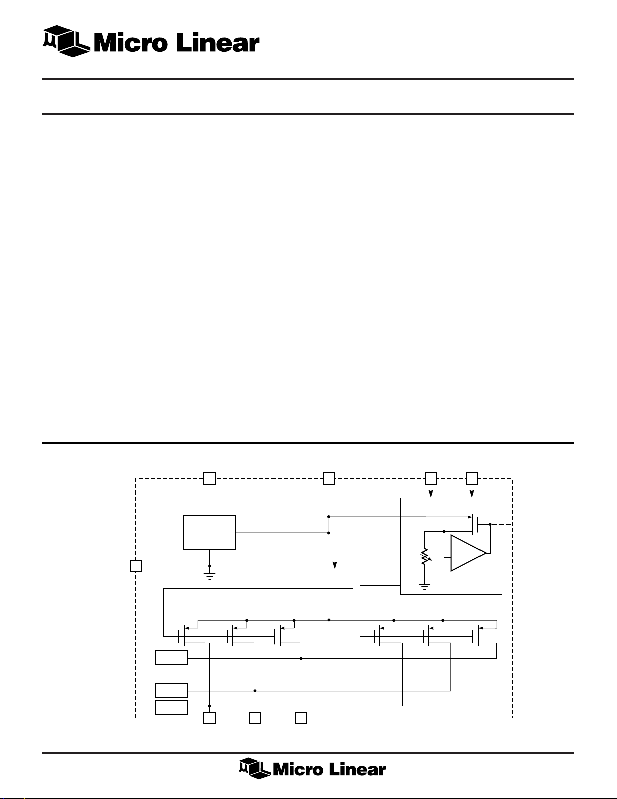
BLOCK DIAGRAM
GND
NCLAMP = Negative Clamp
NCLAMP
. . .
NCLAMP
NCLAMP
TERMPWR
LINEAR
REGULATOR
1V DROPOUT
MOSFETs WITH I
9 TERMINATION LINES
2.85V
NORMAL MODE
MAX
. . .
. . .
216mA
= 24mA
* Some Packages Are End Of Life As Of August 1, 2000
(MAX)
V
REF
MOSFETs WITH I
DISCNKT
2.85V
R
TRIM
LOW POWER MODE
V
MAX
REF
LPWR
CONTROL
BLOCK
= 1mA
. . .
1
Page 2
ML6509
GENERAL DESCRIPTION (Continued)
One unique feature of the ML6509 is its support for a Low
Power mode, for use in Notebook and portable computer
applications, where it provides a 1mA (approximately
2.5KW termination) for less than 6" cable lengths. This
minimizes the battery drain significantly in such systems.
PIN CONFIGURATION
TERMPWR
GND
DISCNKT
LPWR
NC
NC
1
2
3
4
5
6
L1
L2
7
8
16
15
14
13
12
11
10
9
L9
L8
L7
V
REF
L6
L5
L4
L3
Current limiting and thermal shutdown protection are also
provided. The nine line configuration is optimal for wide
SCSI’s 18, 27, or 45 line termination needs.
20-Pin TSSOP16-Pin SOIC
TERMPWR
NC
GND
NC
DISCNKT
LPWR
HS
HS
1
2
3
4
5
6
7
8
L1
L2
9
10
20
19
18
17
16
15
14
13
12
11
L9
L8
HS
L7
V
L6
L5
L4
HS
L3
REF
PIN DESCRIPTION
NAME DESCRIPTION
TERMPWR Termination Power. Should be connected
to the SCSI TERMPWR line. A 10µF
tantalum local bypass capacitor is
recommended per system, as shown in
the application diagram
L1 Signal Termination 1. SCSI bus line 1
L2 Signal Termination 2. SCSI bus line 2
L3 Signal Termination 3. SCSI bus line 3
L4 Signal Termination 4. SCSI bus line 4
L5 Signal Termination 5. SCSI bus line 5
L6 Signal Termination 6. SCSI bus line 6
L7 Signal Termination 7. SCSI bus line 7
L8 Signal Termination 8. SCSI bus line 8
L9 Signal Termination 9. SCSI bus line 9
NOTE : The DISCNKT and LPWR lines have 200ký internal pullup resistors
connected to the supply. These pins should be left floating for normal
operation and should be connected to ground to enable the function.
NAME DESCRIPTION
V
REF
2.85V
Output. External decoupling
REF
with a 10µF tantalum in parallel with a
0.1µF ceramic capacitor is
recommended, as shown in the
application diagram.
DISCNKT Disconnect Terminator. Logic input to
disconnect the terminator from the bus
when the SCSI device no longer needs
termination due to not being the last
device on the bus or otherwise. Active
low input.
LPWR Low Power Mode. Logic input to switch
the terminator mode to a ~2.5kW
termination, with a 1mA drive capability,
meant for power conscious battery
applications which use SCSI devices
supporting cable lengths less than six
inches. Active low input.
GND Ground. Signal Ground (0V)
HS Heat Sink Ground. Should be connected
to GND.
2
Page 3

ML6509
ABSOLUTE MAXIMUM RATINGS
Signal Line Voltage............................. –0.3 to TERMPWR +0.3V
Regulator Output Current ................................... –100 to 300mA
TERMPWR Voltage..................................................... –0.3 to 7V
Storage Temperature .......................................... –65°C to 150°C
Soldering Temperature ..................................... 260°C for 10 sec
Thermal Impedance (q
SOIC .......................................................................... 95°C/W
TSSOP ...................................................................... 110°C/W
)
JA
OPERATING CONDITIONS
TERMPWR Voltage.................................................. 4V to 5.25V
Operating Temperature ........................................... 0°C to 70°C
ELECTRICAL CHARACTERISTICS
Unless otherwise stated, these specifications apply for 4V - TERMPWR - 5.25V, and TA = 0°C to 70°C (Note 1)
PARAMETER CONDITIONS MIN TYP MAX UNITS
SUPPLY
TERMPWR Supply Current L1–L9 = open, DISCNKT = open 3.5 5 mA
L1–L9 = 0.2 V, DISCNKT = open 225 250 mA
DISCNKT = 0 (active) 70 100 µA
DISCNKT
Input Low Voltage LPWR, DISCNKT 1.0 V
Input High Voltage LPWR, DISCNKT TERMPWR V
–1.0
OUTPUT
Output High Voltage Measuring each signal line while 2.8 2.85 2.9 V
other eight are high
Maximum Output Current V
(Normal Mode) line while the other eight are high
Maximum Output Current V
(Lowpower Mode) measuring each signal line while the
Output Clamp Level I
Current Sink Capability V
Output Capacitance L1 thru L9, DISCNKT = 0 4 5 pF
(ML Method) 2V
Output Capacitance L1 thru L9, DISCNKT = 0 6 7 pF
(X3T9.2/855D method) 0.4V
REGULATOR
Output Voltage Sourcing 0–200mA 2.8 2.85 2.9 V
Dropout Voltage L1–L9 = 0.2V, V
Short Circuit Current Regulator output = 0V 100 mA
Thermal Shutdown 170 °C
Note 1: Limits are guaranteed by 100% testing, sampling, or correlation with worst case test conditions.
= 0.2V, Measuring each signal 20 24 mA
OUT
= 0.2V, LPWR = 0, and 0.8 1 1.2 mA
OUT
other eight are high
= –30mA –0.15 0 0.15 V
OUT
= 3.2V (per line) 7 12 mA
OUT
100kHz square wave applied
P-P
biased at 1V D.C.
, 1MHz square wave applied
P-P
biased at 0.5V D.C.
Sinking 0–50mA 2.8 2.85 2.95 V
= 2.85V 1.0 1.2 V
OUT
Regulator output = 5V 300 mA
3
Page 4

ML6509
FUNCTIONAL DESCRIPTION
The SCSI terminator helps in decreasing the transmission
line effects with precise termination. Termination is
conventionally provided at the beginning and end of the
SCSI bus, however when additional peripherals are added,
the termination needs to be disabled from the current
device and enabled on the last device on the bus. Existing
termination schemes use a SIP (Single-In-Line package)
which is plugged into a socket on the PC board of the
SCSI peripheral. To remove the termination, the user
needs to pull the resistor SIP out of its socket. With the
higher levels of system integration, this is no longer a
simple task. With the increasing use of higher data rates
and cable lengths in SCSI subsystems, the need for active
termination is becoming necessary. Active termination
also minimizes power dissipation and can be activated or
deactivated under software control, thus eliminating the
need for end user intervention. The V-I characteristics of
popular SCSI termination schemes are shown in Figure 3.
Theoretically the desired V-I characteristics are the Boulay
type for signal assertion (high to low) and the Ideal type
for signal negation. The ML6509 with its MOSFET based
nonlinear termination element attempts to provide the
most optimum V-I characteristics — optimized for both
signal assertion and negation.
The ML6509 provides active termination for nine signal
lines, thus accommodating basic SCSI which requires 18
lines to be terminated and wide SCSI which requires 27,
36 or 45 lines to be terminated. The ML6509 integrates an
accurate voltage reference (1V dropout voltage) and nine
MOSFET based termination lines. A single internal resistor
is trimmed to tune the V-I characteristic of the MOSFETs as
shown in figure 1. The voltage reference circuit produces
a precise 2.85V level and is capable of sourcing at least
24mA into each of the nine terminating lines when low
(active). When the signal line is negated (driver turns off),
the terminator pulls the signal line to 2.85V (quiescent
state). When all signal lines are inactive, the regulator will
source about 200mA.
The ML6509 SCSI Terminator provides two control
signals, DISCNKT & LPWR which are active low signals
and have an internal 200ký pull-up resistor. The
DISCNKT input when asserted low, isolates the ML6509
from the signal lines and effectively removes the
terminator from the SCSI bus with a disconnect mode
current of less than 100µA. The LPWR input, when
asserted low, puts the ML6509 in the low power
termination mode by providing only a 1mA drive
capability with an effective termination impedance of
2.5kW. This is intended for power conscious portable
systems and peripheral applications where the cable
lengths are small, thus resulting is fast signal transitions
and practically no transmission line effects, while
consuming minimum power (9mA worst case if all lines
were active). At the same time, if this portable system
were connected with an external SCSI peripheral, over a
long cable, the normal terminator mode could be enabled
to ensure compliance with the SCSI standard and maintain
data integrity. In addition the ML6509 provides for
negative clamping of signal transients and also supports
current sink capability in excess of 10mA per signal line
to handle active negation driver overshoot above 2.85V,
a common occurrence with SCSI transceivers. These
functions need to be handled with external components
in SCSI subsystems today. Thus the ML6509 helps in
eliminating a number of external components.
Disconnect mode capacitance is a very critical parameter
in SCSI systems. The ML6509 provides the lowest
capacitance contribution of maximum 5pF which is
guaranteed by production test.
Figure 2 gives an application diagram showing a typical
SCSI bus configuration. To ensure proper operation, the
TERMPWR pin must be connected to the SCSI
TERMPWR line. Each ML6509 requires parallel 0.1µF and
10µF capacitors connected between V
and GND pins
REF
and the TERMPWR line needs a 10µF bypass capacitor
per SCSI system.
3.0V
2.844V
0.3V/div
V
4
NORMAL TERMINATION MODE
IDEAL
ML6509
BOULAY
(SLOPE = 110Ω)
0
3.00mA/div
IL
22.4mA
30.0mA
3.00V
2.85V
0.3V/div
V
0
LOWPOWER TERMINATION MODE
1mA
0.2mA/div
IL
2mA
Figure 1. Trimmed V-I Characteristic of the ML6509
Page 5

Thus in an 8-bit wide SCSI bus arrangement (“A” cable),
two ML6509s would be needed at each end of the SCSI
cable in order to terminate the 18 active signal lines.
16-bit wide SCSI would use three ML6509s, while 32-bit
wide SCSI bus would require five ML6509s.
In a typical SCSI subsystem, the open collector driver in
the SCSI transceiver, when asserted, pulls low and when
negated, the termination resistance serves as the pull-up.
Shown in figure 2 is a typical cable response to a pulse.
The receiving end of the cable will exhibit a single time
delay. When negated, the initial step will reach an
intermediate level defined as V
. With the higher SCSI
STEP
data rates, sampling could occur during this step portion.
In order to get the most noise margin, the step needs to be
as high as possible to prevent false triggering. For this
reason the regulator voltage and the resistor defining the
MOSFETs characteristic is trimmed to ensure that the IO is
as close as possible to the SCSI max current specification.
V
is defined as follows :
STEP
VVIZ
=+×()
STEP OL O O
where
VOL is the Driver output low voltage,
IO is current from receiving terminator
285V
2.7V
2.5V
0.2V
V
ML6509
BOULAY
220/330
TERMINATOR (SOURCE)
DRIVER (SINK)
Figure 3. V-1 Characteristics of Various
SCSI Termination Schemes
ML6509
IDEAL
20mA
40mA
24mA
48mA
I
ZO is characteristic impedance of cable.
TERMPWR LINE
ML6509
TERMPWR
VREF
0.1µF
10µF
SCSI XCVR
DISCNKT
GND
L9 L2 L1
LPWR
. . .
. . .
SCSI CABLE
10µF
ML6509
TERMPWR
DISCNKT
LPWR
. . .
VREF
GND
L9L1 L2
SCSI XCVR
. . .
0.1µF
10µF
SCSI XCVR
V
REG
LINE
ASSERTED
LINE
NEGATED
V
V
V
REG
STEP
OL
Figure 2. Application Diagram Showing Typical SCSI Bus Configuration with the ML6509
5
Page 6

ML6509
This is a very important characteristic that the terminator
helps overcome by increasing the noise margin and
boosting the step as high as possible. This capability for
the ML6509 implementation is illustrated in the attached
simulation graphs which show the terminator performance
under different cable impedance situations and a
comparison is shown with the standard Boulay terminator,
under identical conditions.
2.0V
0.8V
Two Position
DIP Switch
V1(2) = 796.9mV V2(2) = 2.0V ∆V(2) = 1.203V
Figure 4. Transient Response (Actual)
(Approximately 110W, 10 feet long, ribbon cable stock)
TERMPWR
NC
NC
ML6509
GND
DISCNKT
LPWR
L1
L2
L9
L8
L7
V
REF
L6
L5
L4
L3
10µF
0.1µF10µF
TERMPWR
NC
NC
GND
DISCNKT
LPWR
L1
L2
ML6509
2
L9
L8
L7
V
REF
L6
L5
L4
L3
0.1µF
10µF
1
50 Pin SCSI Header Connector
Figure 5. Typical Application Circuit
6
Page 7

DRIVER
END
0.8V
TERMINATOR
END
0.8V
ML6509
ML6509 SCSI TERMINATOR
2V
2V
DRIVER
END
0.8V
TERMINATOR
END
0.8V
100ns 200ns 300ns
TIME (SECONDS)
BOULAY TERMINATOR
2V
2V
100ns 200ns 300ns
TIME (SECONDS)
Conditions Low Cable impedance of 110W (worst case)
tD = 10ns
10 segment distributed L-C, SCSI Bus Model
Driver end of cable not terminated
Figure 6. Signal Assertion/Negation Waveforms (Simulated)
7
Page 8

ML6509
DRIVER
END
0.8V
TERMINATOR
END
0.8V
ML6509 SCSI TERMINATOR
2V
2V
DRIVER
END
0.8V
TERMINATOR
END
0.8V
100ns 200ns 300ns
TIME (SECONDS)
BOULAY TERMINATOR
2V
2V
100ns 200ns 300ns
TIME (SECONDS)
Conditions Low Cable impedance of 55W (worst case)
tD = 10ns
10 segment distributed L-C, SCSI Bus Model
Driver end of cable not terminated
Figure 6a. Signal Assertion/Negation Waveforms (Simulated)
8
Page 9

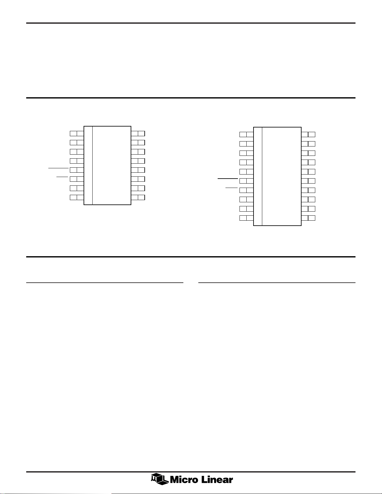
PHYSICAL DIMENSIONS inches (millimeters)
Package: T20
20-Pin TSSOP
0.251 - 0.262
(6.38 - 6.65)
20
ML6509
0.033 - 0.037
(0.84 - 0.94)
1
0.008 - 0.012
(0.20 - 0.30)
PIN 1 ID
0.026 BSC
(0.65 BSC)
0.169 - 0.177
(4.29 - 4.50)
0.043 MAX
(1.10 MAX)
SEATING PLANE
0.246 - 0.258
(6.25 - 6.55)
0.002 - 0.006
(0.05 - 0.15)
0º - 8º
0.020 - 0.028
(0.51 - 0.71)
0.004 - 0.008
(0.10 - 0.20)
9
Page 10

ML6509
PHYSICAL DIMENSIONS inches (millimeters)
Package: S16W
16-Pin Wide SOIC
0.400 - 0.414
16
(10.16 - 10.52)
0.024 - 0.034
(0.61 - 0.86)
(4 PLACES)
0.090 - 0.094
(2.28 - 2.39)
1
PIN 1 ID
0.050 BSC
(1.27 BSC)
0.012 - 0.020
(0.30 - 0.51)
0.291 - 0.301
(7.39 - 7.65)
0.095 - 0.107
(2.41 - 2.72)
SEATING PLANE
0.398 - 0.412
(10.11 - 10.47)
0.005 - 0.013
(0.13 - 0.33)
0º - 8º
0.022 - 0.042
(0.56 - 1.07)
0.009 - 0.013
(0.22 - 0.33)
ORDERING INFORMATION
PART NUMBER TEMPERATURE RANGE PACKAGE
ML6509CS 0°C to 70°C 16-pin SOIC (S16W)
ML6509CT (EOL) 0°C to 70°C 20-pin TSSOP (T20)
© Micro Linear 1997 is a registered trademark of Micro Linear Corporation
Products described herein may be covered by one or more of the following patents: 4,897,611; 4,964,026; 5,027,116; 5,281,862; 5,283,483; 5,418,502; 5,508,570; 5,510,727; 5,523,940; 5,546,017; 5,559,470;
5,565,761; 5,594,376. Other patents are pending.
Micro Linear reserves the right to make changes to any product herein to improve reliability, function or
design. Micro Linear does not assume any liability arising out of the application or use of any product
described herein, neither does it convey any license under its patent right nor the rights of others. The
circuits contained in this data sheet are offered as possible applications only. Micro Linear makes no
warranties or representations as to whether the illustrated circuits infringe any intellectual property rights of
others, and will accept no responsibility or liability for use of any application herein. The customer is urged
to consult with appropriate legal counsel before deciding on a particular application.
10
2092 Concourse Drive
San Jose, CA 95131
Tel: 408/433-5200
Fax: 408/432-0295
DS6509-01
 Loading...