

Page 1

FEDL64P168-01
This version: Sep. 27,1999
Semiconductor
Previous version: Jun.
22,1999
ML64P168
4-Bit Microcontroller with Built-in RC Oscillation Type A/D Converter and LCD Driver
GENERAL DESCRIPTION
The ML64P168 is a one-time-programmable ROM-version product, which has one-time PROM (OTP)
as internal program memory. On the other hand, the ML64168 is a mask ROM-version product, which
has mask ROM as internal program memory.
Unlike the mask ROM-version product (ML64168), the ML64P168 cannot be supplied in the form of a
chip.
The ML64P168 has two operation modes, microcontroller operation mode and PROM mode. The
microcontroller operation mode is used to operate the ML64P168 like a ML64168 and the PROM
mode is used to program or read the PROM.
The ML64P168 is a low power 4-bit microcontroller incorporating the Oki’s original CPU core nX4/30.
The ML64P168 provides a minimum instruction execution time of 4.3µs (@700kHz).
The ML64P168 contains 8160-byte program memory, 512-nibble data memory, three 4-bit input-output
ports, 4-bit input port, 4-bit output port, 2-channel RC oscillation type A/D converter, LCD driver for
up to 120 segments, and buzzer output port.
APPLICATION
The ML64P168 is best suited for low power, high precision thermometers and hygrometers.
FEATURES
∙ Processing speed
Minimum instruction execution time : 4.3 µs @700 kHz
91.6 µs @32.768 kHz
∙ Clock generation circuit
Low-speed clock : 32.768 kHz crystal oscillator
High-speed clock : 700 kHz RC oscillator ( with an external resistor )
CPU clock is selectable as Low-speed clock / High-speed clock by software.
∙ Operating voltage : 1.5 V spec. / 3.0 V spec. ( selectable by mask option )
1.45 to 1.70 V (1.5V spec.)
2.7 to 3.5 V (3.0V spec.)
∙ Operating temperature : 0 to +65°C
The information contained herein can change without notice owing to product and/or technical improvements.
Before using the product, please make sure that the information being referred to is up-to-date.
1/51
Page 2

FEDL64P168-01
Semiconductor
∙ Memory space
Internal program memory : 8160 bytes
Internal data memory : 512 nibbles
∙ RC oscillation type A/D converter : 2 channels
Time division 2-channel method
Counter A : 1 / ( 10
Counter B : 1 / 2
4
× 8 ) × 1
14
× 1
∙ I/O port
Input-output port : 3 ports× 4 bits
Input port : 1 port× 4 bits
Output port : 1 port× 4 bits
( 8 out of the 34 LCD driver outputs can be used as
output-only ports by mask option. )
∙ LCD driver : 34 outputs
(1) At 1/4 duty and 1/3 bias : 120 segments (max.)
(2) At 1/3 duty and 1/3 bias : 93 segments (max.)
(3) At 1/2 duty and 1/2 bias : 64 segments (max.)
Voltage Regulator for LCD Driver (selectable by mask option)
The LCD panel display is stable regardless of temporary supply voltage drop, because the
voltage generated by the voltage regulator for LCD driver is supplied to the bias voltage
generator as a reference voltage.
LCD Operating Voltage
When the voltage regulator for LCD driver is used
: 3.6 V ( Duty cycle = 1/4 or 1/3 )
: 2.4 V ( Duty cycle = 1/2 )
When the voltage regulator for LCD driver is not used
: 4.5 V ( Duty cycle = 1/4 or 1/3 )
: 3.0 V ( Duty cycle = 1/2 )
∙ Buzzer driver : 1 output ( 4 output modes selectable )
∙ Serial port : Synchronous 8-bit transfer
Selectable as external clock / internal clock
Selectable as MSB first / LSB first
∙ Capture circuit : 2 channels ( 32Hz, 64Hz, 128Hz, 256Hz )
∙ Battery check circuit : 1 ( incorporated into the input-only port )
∙ Watchdog timer
∙ Interrupt
External interrupt : 2 sources
Internal interrupt : 8 sources
∙ Package:
80-pin plastic QFP ( QFP80-P-1420-0.80-BK )
Product name : ML64P168 - xxxGP ( written PROM )
ML64P168 - NGP ( blanked PROM )
80-pin plastic QFP ( QFP80-P-1414-0.65-K )
Product name : ML64P168 - xxxGA ( written PROM )
ML64P168 - NGA ( blanked PROM )
xxx indicates a code number.
ML64P168
2/51
Page 3

FEDL64P168-01
Semiconductor
PROGRAM DEVELOPMENT ENVIRONMENT
∙ Structured Assembler : SASM64K
∙ In Circuit Emulator : EASE64168
∙ Debugger : DT64K
ML64P168
3/51
Page 4
FEDL64P168-01
Semiconductor
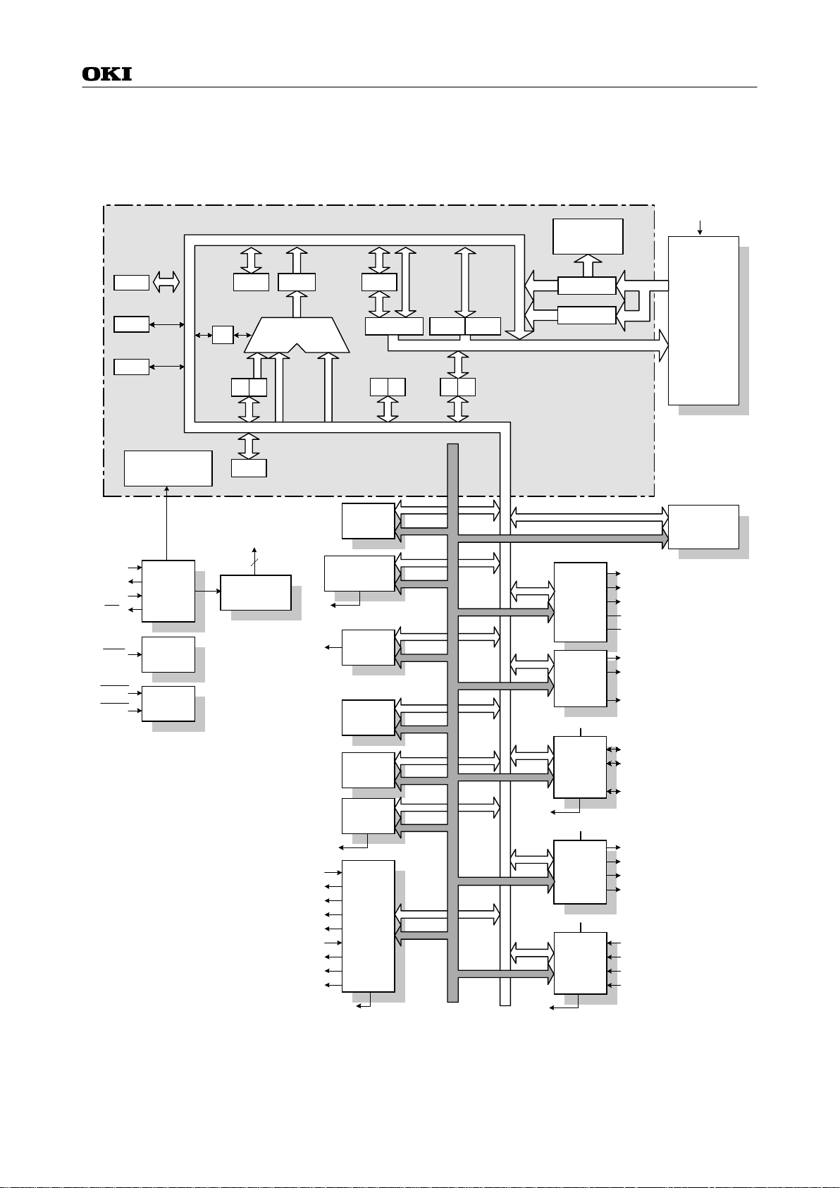
BLOCK DIAGRAM
BSR
MIEF
HALT
TIMING
CONTROLLER
C
B A
SP
CPU CORE: nX-4/30
DATA BUS ( 8 )
TR0
ALU
DATA BUS ( 8 )
TR1TR2
PCH
PCM PCL
X YH L
IR
DECORDER
IR
ROMR
ML64P168
V
PP
PROM
8160
Bytes
OSC1
OSC2
XT
XT
RST
TST1
TST2
2CLK
RSTC
TST
INT
TBC
BC
RAM
512
Nibbles
5
INT
SIOP
ADDRESS BUS
BIAS
V
V
V
C1
DD1
DD2
DD3
C2
BD
BD
LCD
L0
L1
to
L33
IN0
CS0
RS0
CRT0
RT0
IN1
CS1
RS1
RT1
INT
INT
CAPR
INTC
WDT
ADC
INT
INT
V
DDI
P2
P3
P4
V
DDI
P2.0
P2.1
to
P4.3
P1.0
P1
P1.1
P1.2
P1.3
V
DDI
P0.0
P0
P0.1
P0.2
P0.3
4/51
Page 5
FEDL64P168-01
Semiconductor
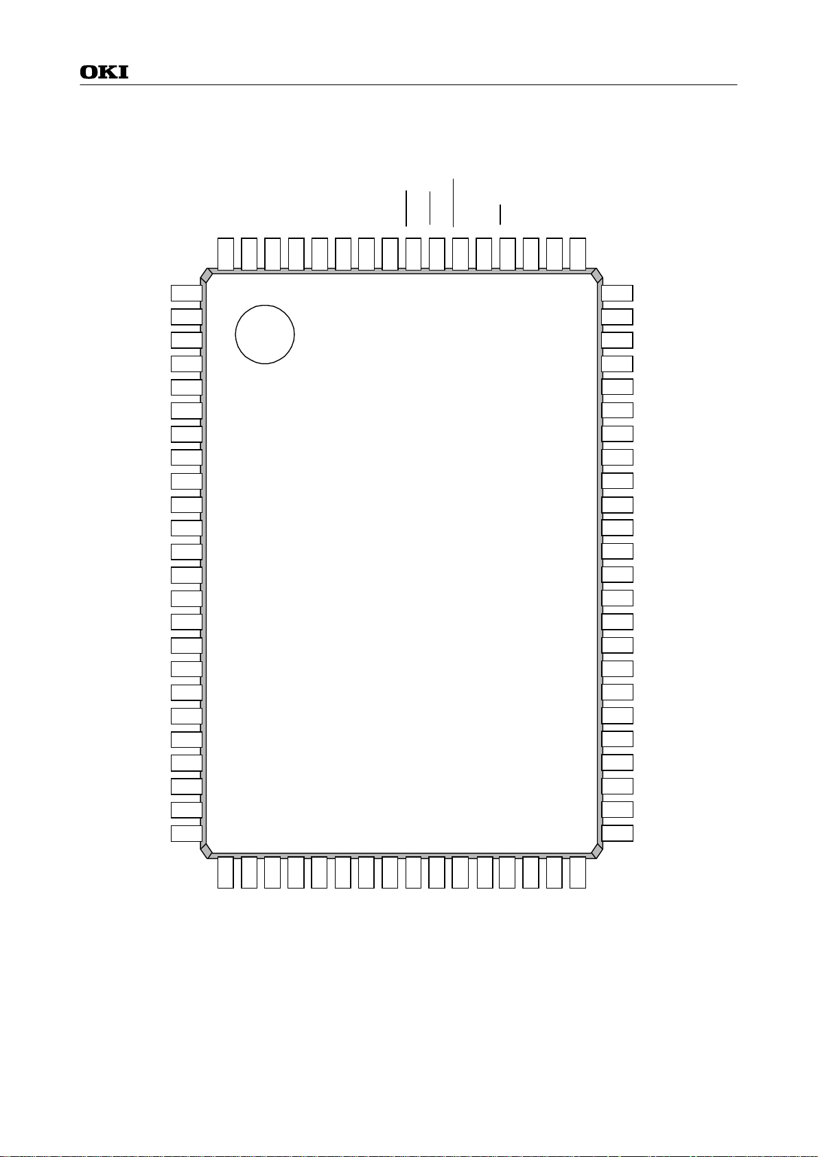
PIN CONFIGURATION (TOP VIEW)
L0
L1
L2
L3
L4
L5
L6
L7
L8
L9
L10
L11
L12
L13
L14
L15
L16
P2.0
P2.1
P2.2
P2.3
P3.0
P3.1
P3.2
P0.3
80
1
2
3
4
5
6
7
8
9
10
11
12
13
14
15
16
17
18
19
20
21
22
23
24
P0.2
79
P0.1
78
P0.0
77
P1.3
76
P1.2
75
P1.1
74
P1.0
73
TST2
72
TST1
71
RESET
XT
70
69
XT
68
DD
V
67
OSC1
OSC2
66
65
64
63
62
61
60
59
58
57
56
55
54
53
52
51
50
49
48
47
46
45
44
43
42
41
ML64P168
L33 / P6.3
L32 / P6.2
L31 / P6.1
L30 / P6.0
L29 / P5.3
L28 / P5.2
L27 / P5.1
L26 / P5.0
L25
L24
L23
L22
L21
L20
L19
L18
L17
C2
C1
DD3
V
DD2
V
DDI
V
DD1
V
RT1
25
P3.3
26
P4.0
27
28
29
30
31
32
33
34
PPVSS
BD
P4.1
P4.2
P4.3
V
RT0
CRT0
( GP : QFP80-P-1420-0.80-BK )
80-Pin Plastic QFP
35
RS0
36
CS0
37
IN0
38
IN1
39
CS1
40
RS1
5/51
Page 6
FEDL64P168-01
Semiconductor
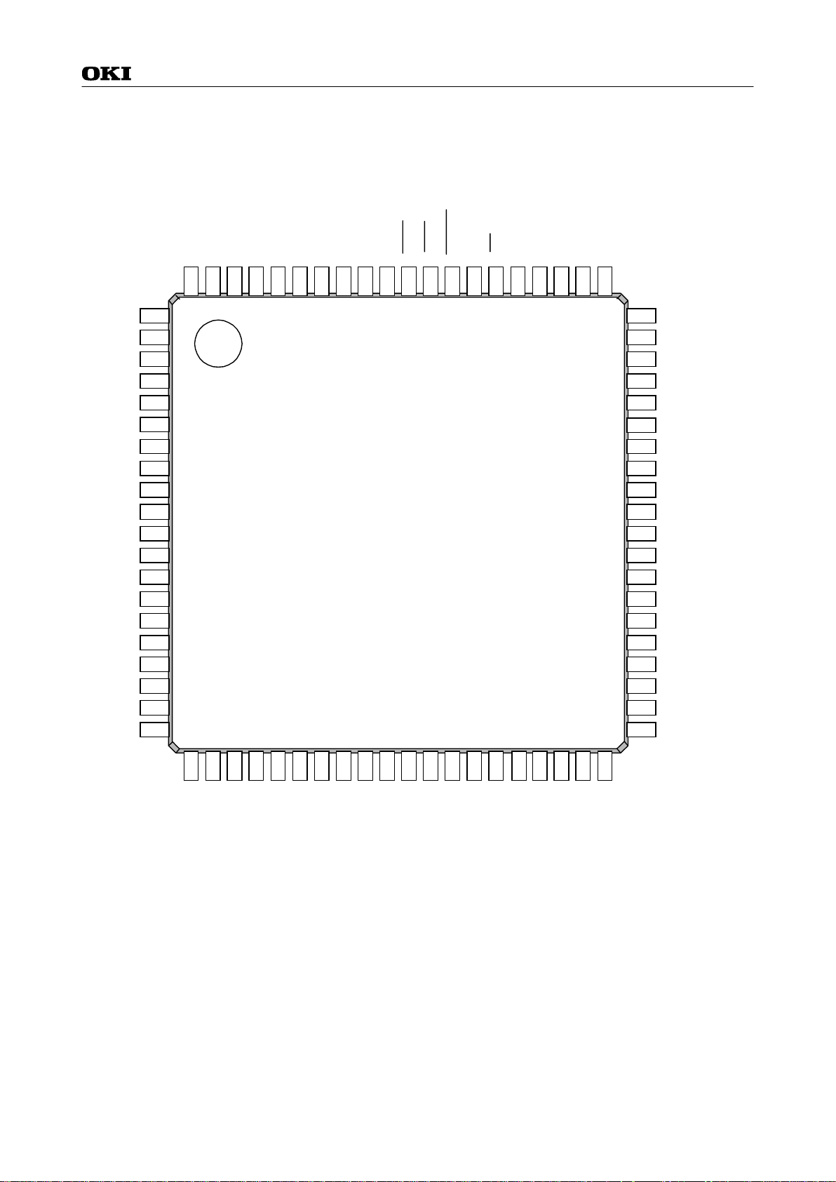
PIN CONFIGURATION (TOP VIEW) ( continued )
L1
L0
L2
L3
L4
L5
L6
L7
L8
L9
L10
L11
L12
L13
L14
L15
L16
P2.0
P2.1
P2.2
P2.3
P3.0
10
11
12
13
14
15
16
17
18
19
20
P0.3
80
79
78
1
2
3
4
5
6
7
8
9
P0.2
77
P0.1
76
P0.0
75
P1.3
74
P1.2
73
P1.1
72
P1.0
71
TST2
70
TST1
69
RESET
XT
68
67
XT
66
DD
V
65
OSC1
64
OSC2
63
L33 / P6.3
L32 / P6.2
62
61
60
59
58
57
56
55
54
53
52
51
50
49
48
47
46
45
44
43
42
41
ML64P168
L31 / P6.1
L30 / P6.0
L29 / P5.3
L28 / P5.2
L27 / P5.1
L26 / P5.0
L25
L24
L23
L22
L21
L20
L19
L18
L17
C2
C1
V
DD3
V
DD2
V
DDI
21
P3.1
22
P3.2
23
P3.3
24
P4.0
25
26
27
28
29
30
31
32
PPVSS
BD
P4.1
P4.2
P4.3
V
RT0
CRT0
( GA : QFP80-P-1414-0.65-K )
80-Pin Plastic QFP
33
RS0
34
CS0
35
IN0
36
IN1
37
CS1
38
RS1
39
RT1
40
DD1
V
6/51
Page 7

FEDL64P168-01
Semiconductor
ML64P168
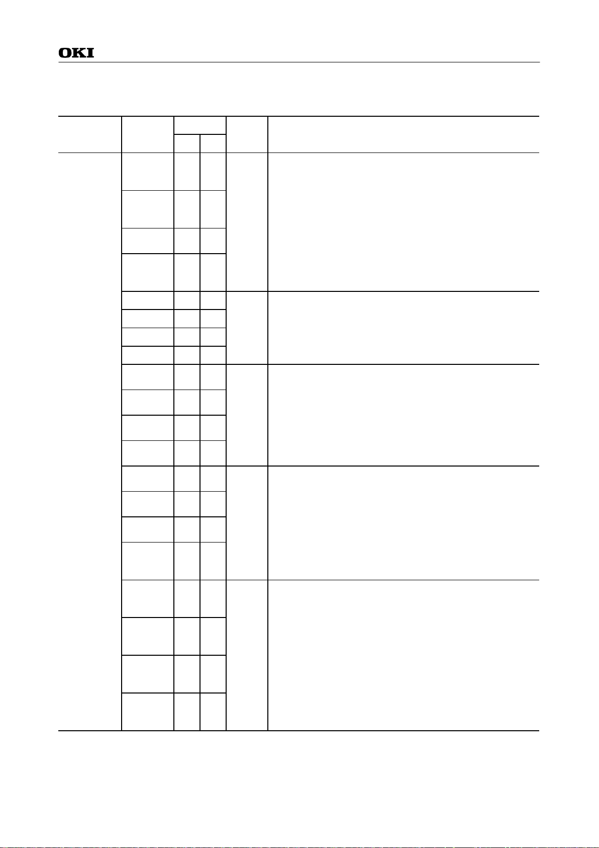
PIN DESCRIPTIONS
The basic functions of each pin of the ML64P168 is described in Table 1.
A symbol with a slash ( / ) denotes a pin that has a secondary function.
Refer to Table 2 for secondary functions.
For Type, “ - ” denotes a power supply pin, “ I ” an input pin, “O” an output pin, and “I/O” an inputoutput pin.
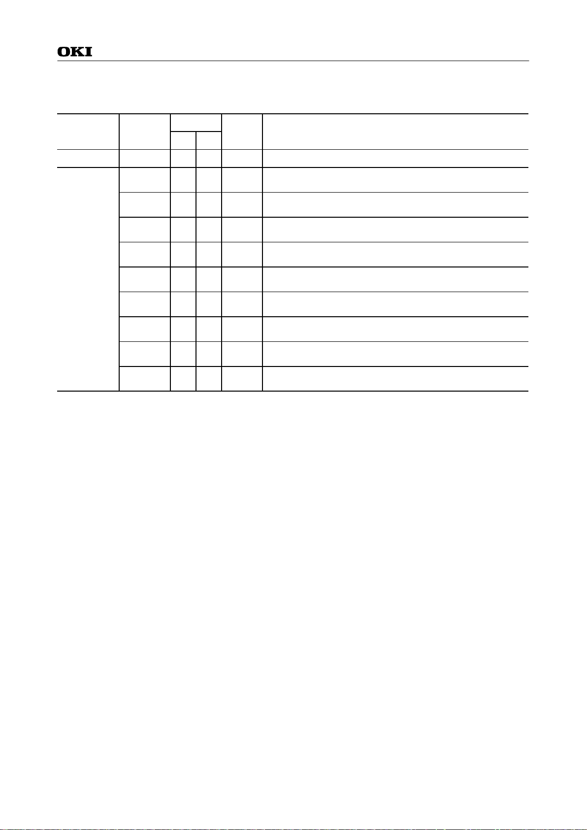
Table 1 Pin Descriptions ( Basic Functions )
Function Symbol
SS
V
DD
V
DD1
V
DD2
V
Power
Supply
DD3
V
DDI
V
Pin No.
GP GA
Type Description
32 30 - 0V power supply
67 65 - Positive power supply
42 40 -
44 42 -
45 43 -
Bias output for driving LCD (+1.5 V, +1.2 V* )
Bias output for driving LCD (+3.0 V, +2.4 V* )
Bias output for driving LCD (+4.5 V, +3.6 V* )
43 41 - Positive power supply for I/O port interface
PP
V
C1 46 44 -
C2 47 45 -
XT
XT 68 66 O
31 29 - Power supply (+12.5 V) for PROM writing
Pins for connecting a capacitor for generating LCD driving
bias
69 67 I
Low-speed clock oscillation input and output pins.
Connect to a crystal ( 32.768 kHz ).
Oscillation
Test
OSC1 66 64 I
OSC2 65 63 O
TST1
TST2
71 69 I
72 70 I
High-speed clock oscillation input and output pins.
Connect to an external resistor for oscillation ( R
Input pins for testing.
A pull-up resistor is internally connected to these pins.
System reset input pin.
Reset
RESET
70 68 I
Setting this pin to ″ L ″ level puts this device into a reset state.
Then, setting this pin to ″ H ″ level starts executing an
instruction from address 0000H.
*When the voltage regulator for LCD driver is used.
OS
).
7/51
Page 8
FEDL64P168-01
Semiconductor
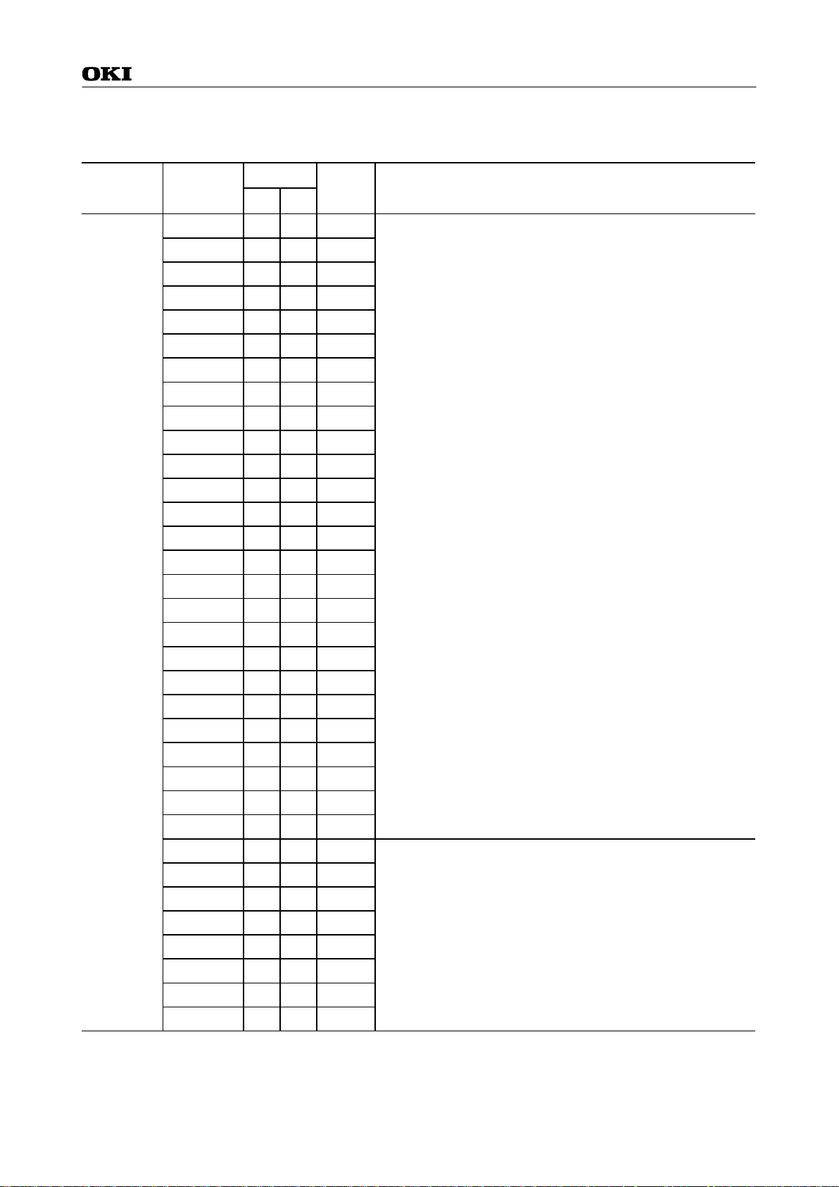
Table 1 Pin Descriptions ( Basic Functions ) ( continued )
Function Symbol
P0.0/
INT1/
CAPIN0
P0.1/
INT1/
CAPIN1
P0.2/
INT1
P0.3/
INT1/
CMP
P1.0 73 71
P1.1 74 72
P1.2 75 73
Pin No.
GP GA
77 75
78 76
79 77
80 78
Type Description
4-bit input port ( Port 0 )
Selectable as pull-up resistor input, pull-down resistor input,
or high impedance input by the port 01 control register
( P01CON ).
I
4-bit output port ( Port 1 )
Selectable as NMOS open drain output or CMOS output by
O
the port 01 control register ( P01CON ).
P1.0 is a high current drive output port.
ML64P168
Ports
P1.3 76 74
P2.0/
INT0
P2.1/
INT0
P2.2/
INT0
P2.3/
INT0
P3.0/
INT0
P3.1/
INT0
P3.2/
INT0
18 16
19 17
20 18
21 19
22 20
23 21
24 22
P3.3/
INT0/
25 23
SIN
P4.0/
INT0/
26 24
SOUT
P4.1/
INT0/
27 25
SPR
P4.2/
INT0/
28 26
SCLK
P4.3/
INT0/
29 27
MON
I/O
I/O
I/O
4-bit input-output port ( Port 2 )
Fllowing can be specified for each bit by the port 2 control
registers 0 to 3 ( P20CON to P23CON ).
(1) input or output
(2) pull-up/pull-down resistor input or high impedance input
(3) NMOS open drain output or CMOS output
4-bit input-output port ( Port 3 )
Following can be specified for each bit by the port 3 control
registers 0 to 3 ( P30CON to P33CON ).
(1) input or output
(2) pull-up/pull-down resistor input or high impedance input
(3) NMOS open drain output or CMOS output
4-bit input-output port ( Port 4 )
Following can be specified for each bit by the port 4 control
registers 0 to 3 ( P40CON to P43CON ).
(1) input or output
(2) pull-up/pull-down resistor input or high impedance input
(3) NMOS open drain output or CMOS output
8/51
Page 9
FEDL64P168-01
Semiconductor
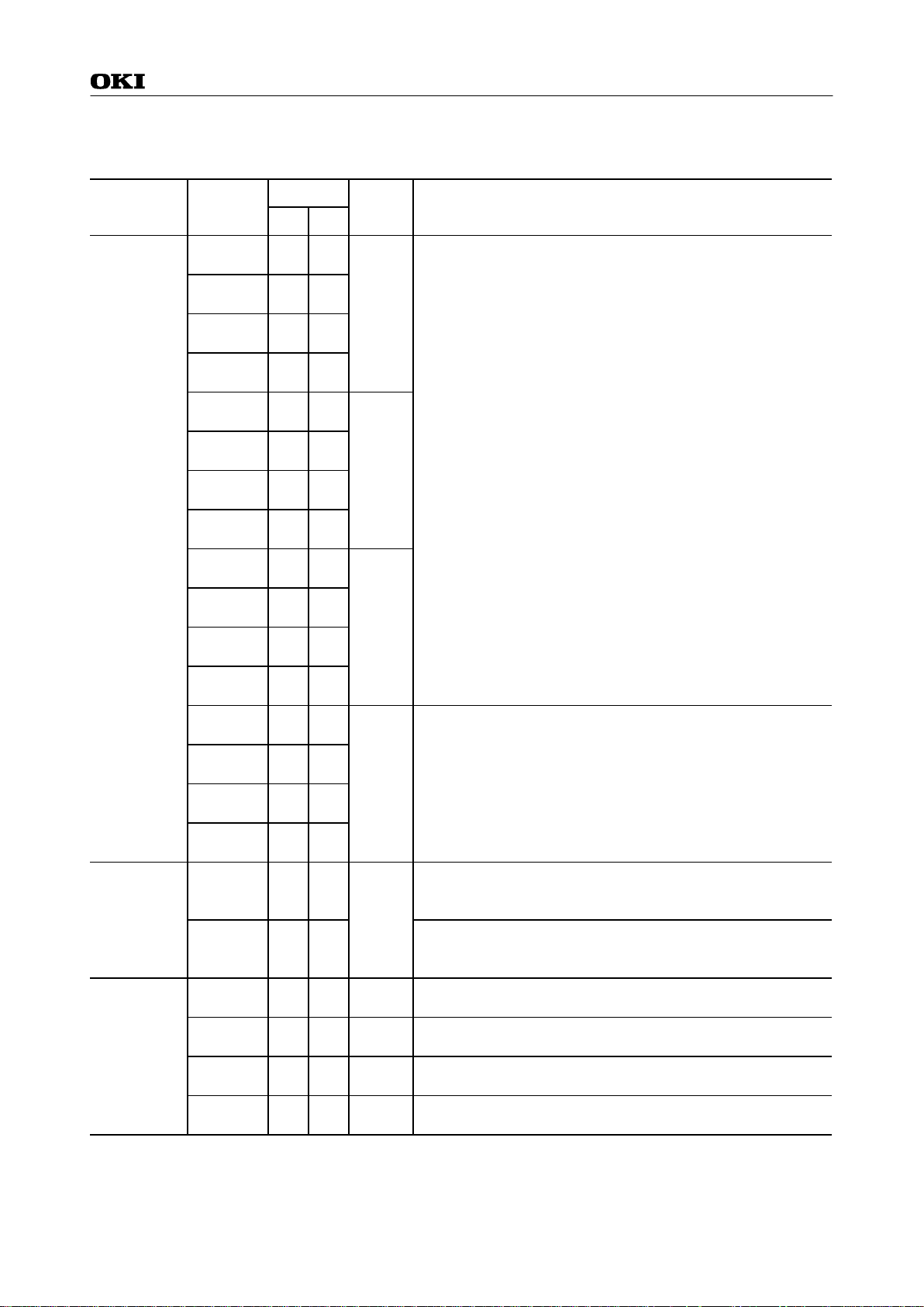
Table 1 Pin Descriptions ( Basic Functions ) ( continued )
Function Symbol
Buzzer BD 30 28 O Output pin for the buzzer driver.
RT03331O
CRT0 34 32 O
RS0 35 33 O
CS0 36 34 O
A/D
Converter
IN0 37 35 I
RT14139O
RS1 40 38 O
CS1 39 37 O
IN1 38 36 I
Pin No.
GP GA
Type Description
Resistance temperature sensor connection pin
( for channel 0 )
Resistance/capacitance temperature sensor connection pin
( for channel 0 )
Reference resistor connection pin
( for channel 0 )
Reference capacitor connection pin
( for channel 0 )
Input pin for RC oscillator circuit
( for channel 0 )
Resistance temperature sensor connection pin
( for channel 1 )
Reference resistor connection pin
( for channel 1 )
Reference capacitor connection pin
( for channel 1 )
Input pin for RC oscillator circuit
( for channel 1 )
ML64P168
9/51
Page 10
FEDL64P168-01
Semiconductor
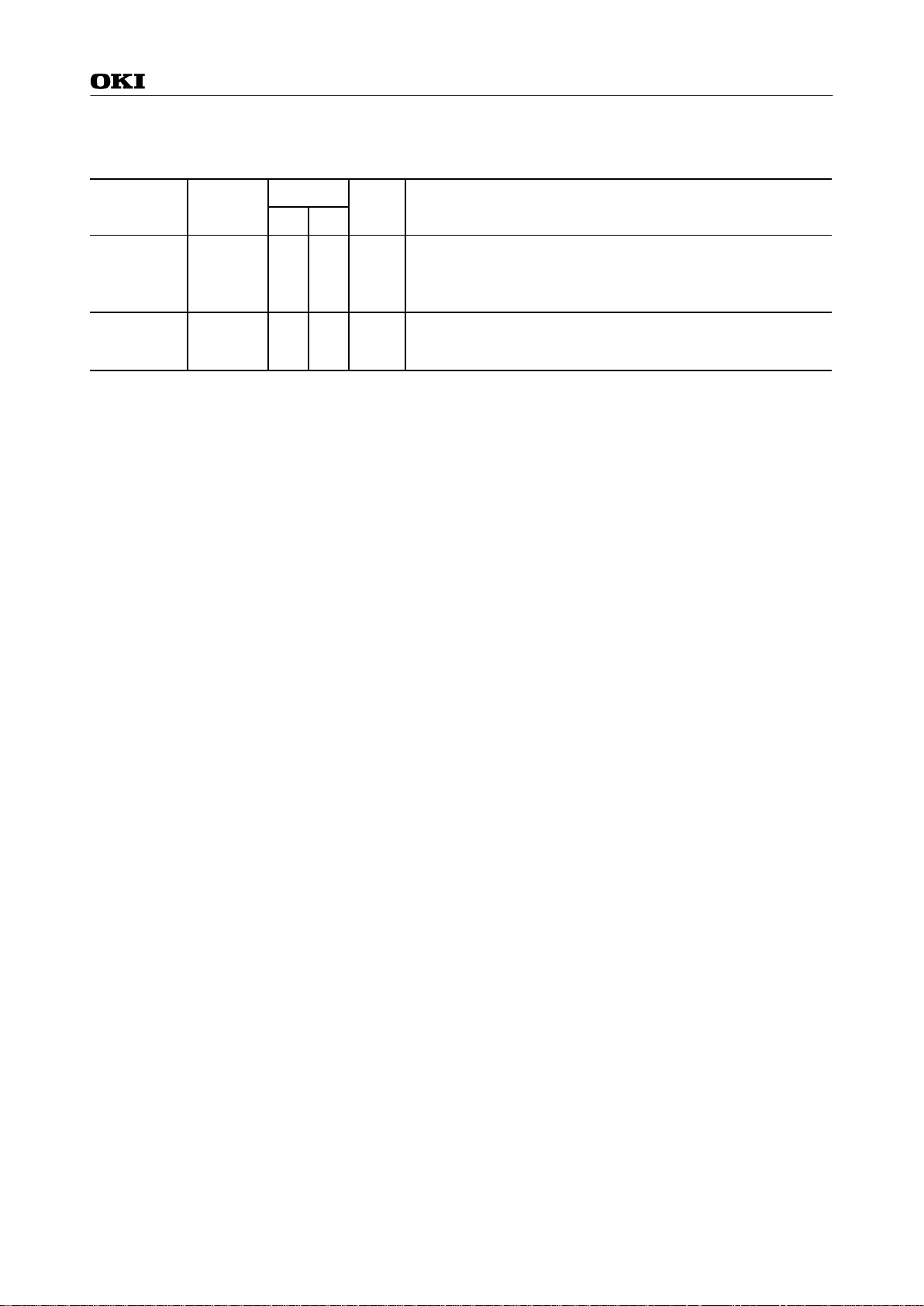
Table 1 Pin Descriptions ( Basic Functions ) ( continued )
Function Symbol
L0 1 79 O
L1 2 80 O
L2 3 1 O
L3 4 2 O
L4 5 3 O
L5 6 4 O
L6 7 5 O
L7 8 6 O
L8 9 7 O
L9 10 8 O
L10 11 9 O
Pin No.
GP GA
ML64P168
Type Description
LCD segment and common signals output pins.
LCD
Driver
L11 12 10 O
L12 13 11 O
L13 14 12 O
L14 15 13 O
L15 16 14 O
L16 17 15 O
L17 48 46 O
L18 49 47 O
L19 50 48 O
L20 51 49 O
L21 52 50 O
L22 53 51 O
L23 54 52 O
L24 55 53 O
L25 56 54 O
L26 / P5.0 57 55 O
L27 / P5.1 58 56 O
L28 / P5.2 59 57 O
LCD segment and common signals output pins.
These pins can be configured to be output ports by a mask
option.
L29 / P5.3 60 58 O
L30 / P6.0 61 59 O
L31 / P6.1 62 60 O
L32 / P6.2 63 61 O
L33 / P6.3 64 62 O
10/51
Page 11
FEDL64P168-01
Semiconductor
Function Symbol
P2.0/
INT0
P2.1/
INT0
P2.2/
INT0
P2.3/
INT0
P3.0/
INT0
P3.1/
INT0
P3.2/
INT0
P3.3/
External
Interrupt
INT0
P4.0/
INT0
P4.1/
INT0
P4.2/
INT0
P4.3/
INT0
P0.0/
INT1
P0.1/
INT1
P0.2/
INT1
P0.3/
INT1
P0.0/
Capture
trigger
CAPIN0
P0.1/
CAPIN1
P3.3/
SIN
P4.0/
Serial
port
SOUT
P4.1/
SPR
P4.2/
SCLK
Table 2 Pin Descriptions ( Secondary Functions )
Pin No.
GP GA
18 16
19 17
20 18
21 19
22 20
23 21
24 22
25 23
26 24
27 25
28 26
29 27
77 75
78 76
79 77
80 78
77 75
78 76
25 23 I
26 24 O
27 25 O
28 26 I/O
Type Description
Secondary functions of P2.0 to P2.3, P3.0 to P3.3, and P4.0
to P4.3:
Level-triggered external 0 interrupt input pins.
The change of input signal level causes an interrupt to occur.
I
I
I
Secondary functions of P0.0 to P0.3:
Level-triggered external 1 interrupt input pins.
The change of input signal level causes an interrupt to occur.
I
Secondary functions of P0.0:
This pin is assigned the capture circuit trigger input pin of
CAPR0 function .
I
Secondary functions of P0.1:
This pin is assigned the capture circuit trigger input pin of
CAPR1 function .
Secondary functions of P3.3:
This pin is assigned the data input of a serial port.
Secondary functions of P4.0:
This pin is assigned the data output of a serial port.
Secondary functions of P4.1:
This pin is assigned the ready output of a serial port.
Secondary functions of P4.2:
This pin is assigned the clock input-output of a serial port.
ML64P168
11/51
Page 12
FEDL64P168-01
Semiconductor
Table 2 Pin Descriptions ( Secondary Functions ) ( continued )
Function Symbol
RC
Oscillation
Monitor
Battery
Check
P4.3/
MON
P0.3/
CMP
Pin No.
GP GA
Type Description
29 27 O
80 78 I
ML64P168
Secondary functions of P4.3:
This pin is a monitor output of the RC oscillation clock for an
A/D converter and a 700kHz RC oscillation clock for a system
clock.
Secondary functions of P0.3:
This pin is an analog comparator input pin for battery check
circuit.
12/51
Page 13
FEDL64P168-01
Semiconductor
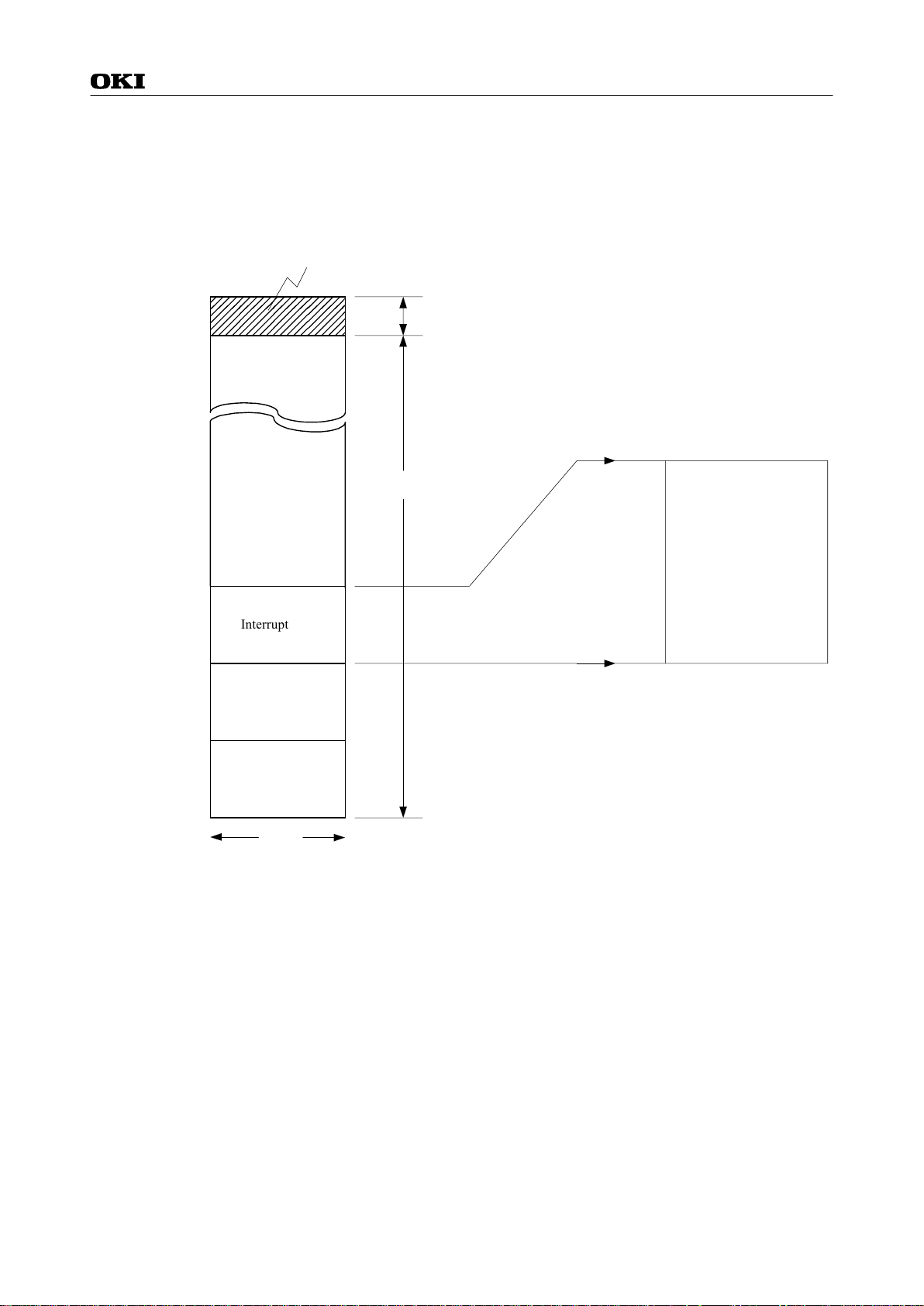
MEMORY MAPS
Program Memory ( PROM )
1FFFH
1FE0H
003EH
Interrupt area
0020H
Test program area
8160 bytes
ML64P168
32 bytes
Contents of interrupt area
003BH Watchdog interrupt
0038H External 0 interrupt
0035H Serial port interrupt
0032H External 1 interrupt
002FH A/D converter interrupt
002CH 256Hz interrupt
0029H 32Hz interrupt
0026H 16Hz interrupt
0023H 1Hz interrupt
0020H 0.1Hz interrupt
CZP area
0010H
0000H
Start address
8 bits
Program Memory Map
Address 0000H is the instruction execution start address by the system reset.
The CZP area from address 0010H to address 001FH is the start address for the CZP subroutine of 1byte call instruction.
The start address of interrupt subroutine is assigned to the interrupt address from address 0020H to
003DH.
The user area has 8160 bytes of address 0000H to 1FDFH. No program can be stored in the test
program area.
13/51
Page 14
FEDL64P168-01
Semiconductor
ML64P168
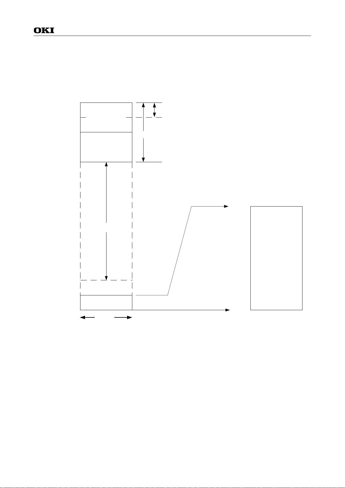
Data Memory
The data memory area consists of 8 banks and each bank has 256 nibbles ( 256 × 4 bits ).
The data RAM is assigned to BANK 6, BANK 7 and peripheral ports are assigned to BANK 0.
7FFH
780H
700H
6FFH
600H
BANK7
Data RAM area
( 256 nibbles )
512 nibbles
BANK6
Data RAM area
( 256 nibbles )
Data / Stack area ( 128 nibbles )
Contents of 000H to 07FH
07FH
Inaccessible area
SFR area
100H
0FFH
080H
07FH
000H
Unused area
BANK0
000H
4 bits
Data Memory Map
Half the BANK 7 of Data RAM area ( 128 nibbles ) is shared by the stack area. The stack is a memory
starting from address 7FFH toward the low-order addresses where 4 nibbles are used by Subroutine
Call Instruction and 8 nibbles are used by an interrupt.
The addresses 080H to 0FFH of BANK 0 are not assigned as the data memory, so access to these
addresses has no effect. Moreover, it is impossible to access BANK 1 to BANK 5.
14/51
Page 15
FEDL64P168-01
Semiconductor
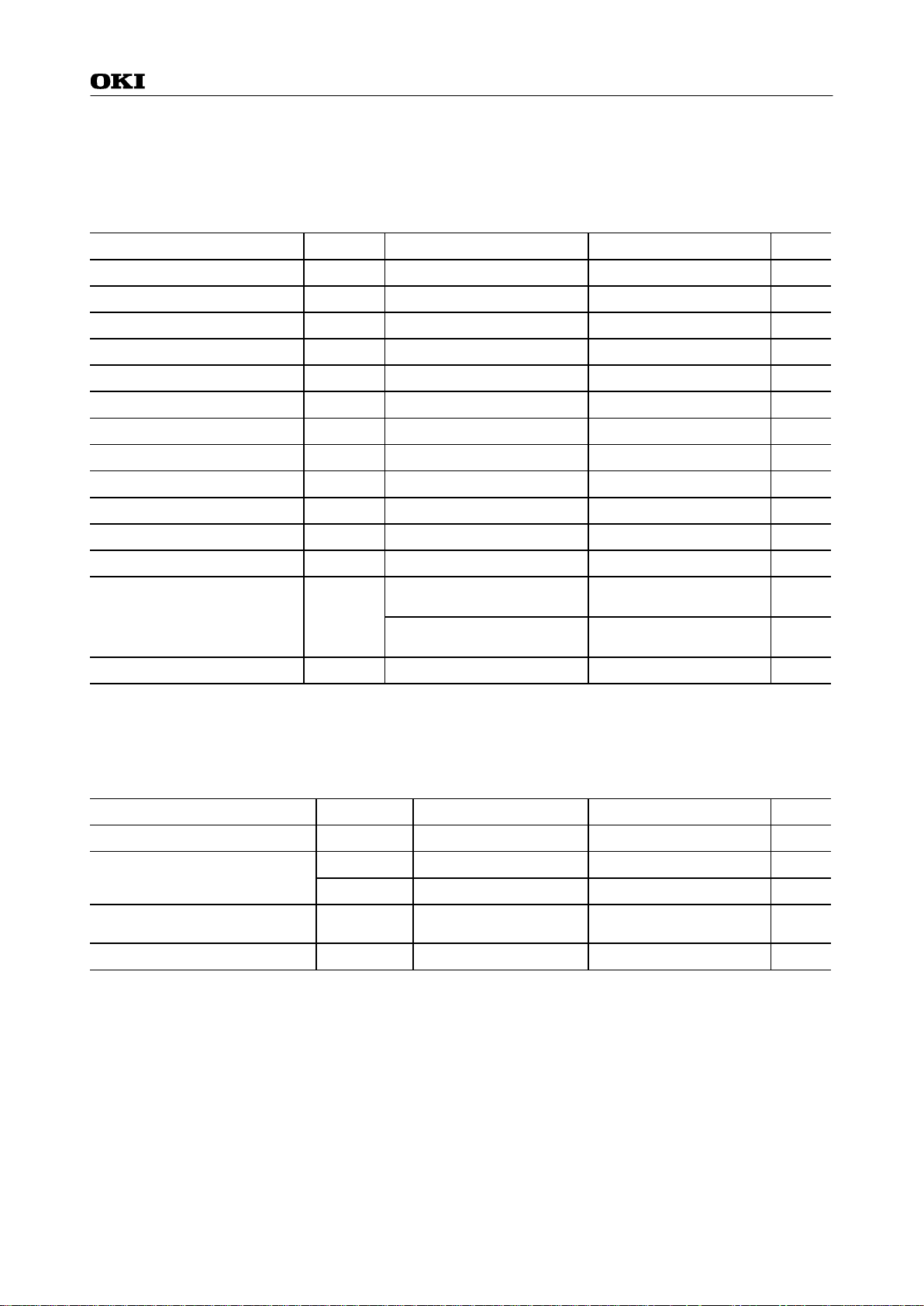
ABSOLUTE MAXIMUM RATINGS ( 1.5
Parameter Symbol Condition Rating Unit
Power supply voltage 1 V
Power supply voltage 2 V
Power supply voltage 3 V
Power supply voltage 4 V
Power supply voltage 5 V
Input voltage 1 V
Input voltage 2 V
Output voltage 1 V
Output voltage 2 V
Output voltage 3 V
Output voltage 4 V
Output voltage 5 V
Power Dissipation PD
Storage temperature T
DD1
DD2
DD3
DDI
DD
IN1
IN2
OUT1
OUT2
OUT3
OUT4
OUT5
STG
VDD input, Ta = 25°C
DDI
V
DD1
V
DD2
V
DD3
V
VDD output, Ta = 25°C
DDI
V
QFP80-P-1420-0.80-BK
QFP80-P-1414-0.65-K
V Spec. )
(VSS = 0V)
Ta = 25°C -0.3 to + 2.0 V
Ta = 25°C -0.3 to + 4.0 V
Ta = 25°C
Ta = 25°C
Ta = 25°C
-0.3 to + 5.5 V
-0.3 to + 5.5 V
-0.3 to + 2.0 V
-0.3 to VDD+ 0.3 V
input, Ta = 25°C
output, Ta = 25°C
output, Ta = 25°C
output, Ta = 25°C
-0.3 to V
-0.3 to V
-0.3 to V
-0.3 to V
DDI
+ 0.3 V
DD1
+ 0.3 V
DD2
+ 0.3 V
DD3
+ 0.3 V
-0.3 to VDD+ 0.3 V
output, Ta = 25°C
Ta = 0 to + 65°C
Ta = 0 to + 65°C
-0.3 to VDD+ 0.3 V
381 mW
334 mW
- -55 to + 150
ML64P168
°
C
RECOMMENDED OPERATING CONDITIONS ( 1.5V Spec. )
Parameter Symbol Condition Rating Unit
VDD,V
DDI
V
R
XT
op
OS
DD1
-0 to + 65
- 1.45 to 1.70 V
- 2.70 to 5.25 V
- 60 to 200
- 30 to 35 kHz
Operating Temperature* T
Operating Voltage*
External 700kHz RC Oscillator
Resistance*
Crystal oscillation frequency* f
* : At Non-regulated LCD driver.
In case of select a voltage regulated LCD driver, see P.37/51.
(VSS = 0V)
°
C
Ω
k
15/51
Page 16
FEDL64P168-01
Semiconductor
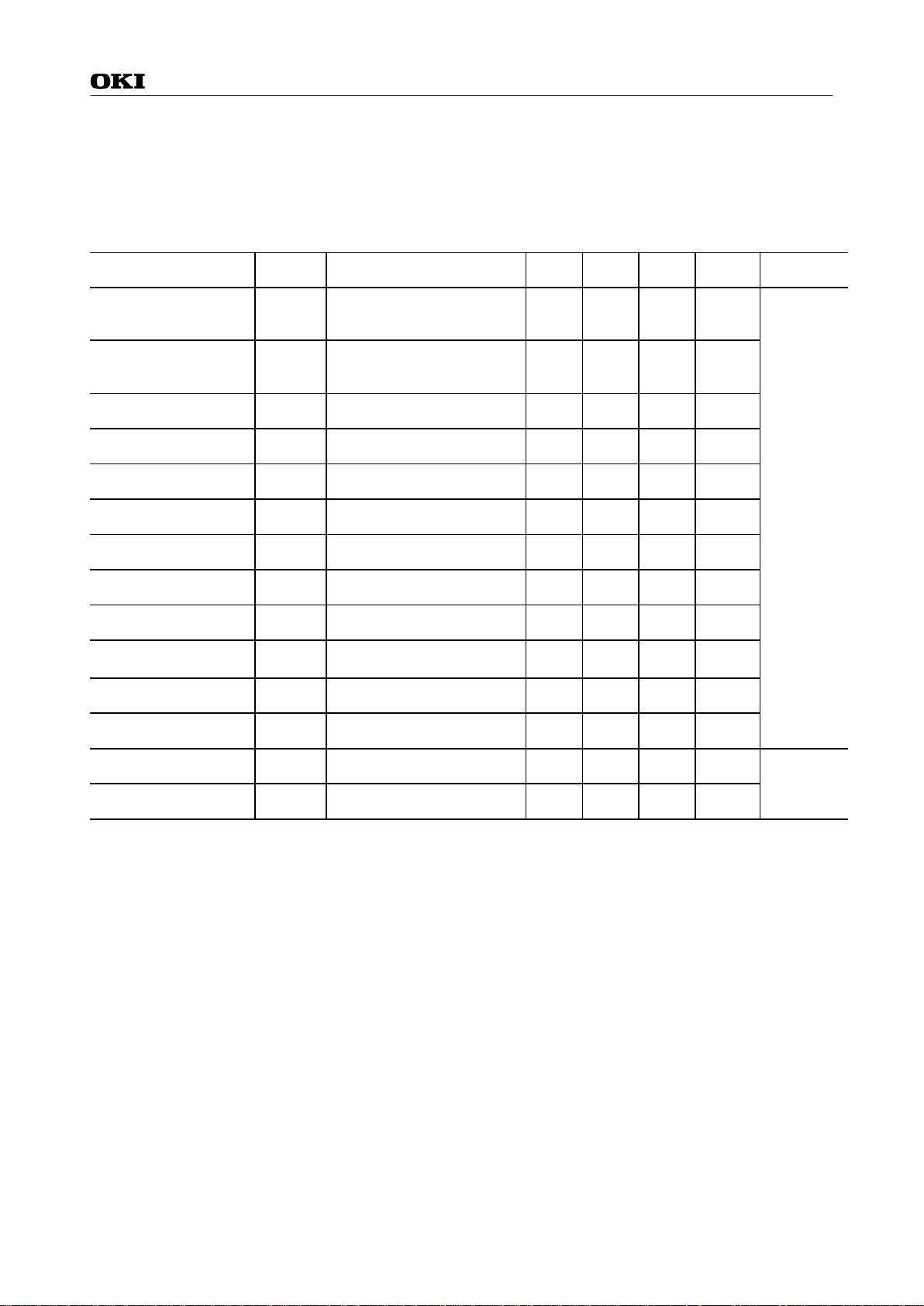
ELECTRICAL CHARACTERISTICS ( 1.5
DC Characteristics ( 1.5 V Spec. )
(VSS=0V, V
Parameter Symbol Condition Min. Typ. Max. Unit
DD2
V
Vo l t a ge * V
DD3
V
Vo l t a ge * V
Crystal Oscillation
Start Voltage
Crystal Oscillation
Hold Voltage
Crystal Oscillation
Stop Detection Time
Internal Crystal
Oscillator Capacitance
External Crystal
Oscillator Capacitance
Internal Crystal
Oscillator Capacitance
Internal 700kHz RC
Oscillator Capacitance
700kHz RC Oscillation
Frequency
POR Generation
Vo l t a g e
POR Non-generation
Vo l t a g e
Battery Check
Reference Voltage
VRB Temperature
Va r ia t i o n
V
V
T
C
V
V
∆
DD2
DD3
STA
HOLD
STOP
C
GEX
C
OS
C
OSC
f
POR1
POR2
RB
V
V
Ca, Cb, C12=0.1µF
Ca, Cb, C12=0.1µF
Oscillation start time:
within 5 seconds
G
When external CG used 10 - 30 pF
D
External resistor ROS=160k
VDD = 1.45 to 1.70V
When VDD is between
POR1
V
and 1.5V
No POR when VDD is
between V
Ta = 25°C
RB
DD1=VDD
-
-
-
-101520pF
- 8 12 16 pF
POR2
and 1.5V
-
V Spec. )
=1.5V, V
+100%
-50%
+100%
-50%
Ω
ML64P168
DDI
=2.7V, Ta=0 to +65°C unless otherwise specified )
Measuring
Circuit
2.8 3.0 3.2 V
4.3 4.5 4.7 V
1.47 - - V
1.40 - - V
0.1 - 1000 ms
10 15 20 pF
80 280 350 kHz
0-0.4V
1.4 - 1.5 V
0.50 0.60 0.70 V
--2-
mV/°C
1
2
Notes: 1.”POR” denotes Power On Reset.
STOP
2.”T
” indicates that if the crystal oscillator stops over the value of T
* : At Non-regulated LCD driver.
In case of select a voltage regulated LCD driver, see P.37/51.
STOP
, the system reset occurs.
16/51
Page 17

FEDL64P168-01
Semiconductor
DC Characteristics ( 1.5V Spec. ) ( Continued )
SCK
=300kHz,
DD1=VDD
=1.5V, V
(VSS=0V, V
Parameter Symbol Condition Min. Typ.
Supply current 1* I
Supply current 2* I
Supply current 3 I
Supply current 4 I
Supply current 5 I
Supply current 6 I
DD1
DD2
DD3
DD4
DD5
DD6
CPU in halt state
(700kHz RC oscillation stop)
CPU in operating state
(700kHz RC oscillation stop)
CPU in operating state
(700kHz RC oscillation in operation)
Serial transfer, f
CPU in operating state
(700kHz RC oscillation stop)
CPU in halt state
(700kHz RC oscillation
stop)
RC oscillation for A/D
converter is in operating
state
Battery check circuit in operating state,
CPU in operating state
(700kHz RC oscillation stop)
RT0=10k
T0
=2k
R
DDI
=2.7V, Ta=0 to +65°C unless otherwise specified )
Ω
Ω
Max
.
-25
-1530
- 200 300
- 60 100
- 150 230
- 600 900
- 25 125
ML64P168
Unit
µ
A
µ
A
µ
A
µ
A
µ
A
µ
A
µ
A
Measur-
ing
Circuit
1
* : At Non-regulated LCD driver.
In case of select a voltage regulated LCD driver, see P.37/51.
17/51
Page 18

FEDL64P168-01
Semiconductor
DC Characteristics (1.5 V Spec. ) ( Continued )
(VSS=0V, V
DD1=VDD
=1.5V, V
Parameter Symbol Condition Min. Typ. Max. Unit
Output current 1
( P1.0 )
Output current 2
( P1.1 to P1.3 )
OH1
I
OL1
I
OH1S
I
OL1S
I
OH2
I
OL2
I
OH1
V
= V
OL1
V
= 0.5V 2 5 20
DDI
V
= 5.0V, V
DDI
V
= 5.0V, V
OH2
V
= V
OL2
V
= 0.5V 0.7 2.0 6.0
( P2.0 to P2.3 )
( P3.0 to P3.3 )
( P4.0 to P4.3 )
Output current 3
( BD )
Output current 4
OH2S
I
OL2S
I
OH3
I
OL3
I
OH4
I
DDI
V
= 5.0V, V
DDI
V
= 5.0V, V
OH3
V
= VDD - 0.7V -1.8 -0.6 -0.1
OL3
V
= 0.7V 0.2 2 4
OH4
V
= VDD - 0.1V -1.1 -0.6 -0.2
( RT0, RT1, RS0,
RS1, CRT0, CS0,
CS1 )
Output current 5
( When the pins
I
I
I
OL4
OH5
OL5
OL4
V
= 0.1V 0.3 0.6 1.1
OH5
V
= V
OL5
V
= 0.5V 0.15 1.0 4
L26 to L33 are
configured as
output ports )
Output current 6
( OSC2 )
OH5S
I
OL5S
I
OH6
I
OL6
I
OH7
I
DDI
V
= 5V, V
DDI
V
= 5V, V
OH6
V
= V
OL6
V
= 0.5V 0.15 0.7 2.1
OH7
V
= V
DD2
=3.0V, V
DDI
- 0.5V -6.0 -1.7 -0.7
OH1S
OL1S
DDI
- 0.5V -6.0 -2.0 -0.7
OH2S
OL2S
DDI
- 0.5V -1.5 -0.8 -0.15
OH5S
= V
OL5S
= 0.5V 0.2 3.0 5.0
DD
- 0.5V -2.1 -0.7 -0.15
DD3
- 0.2V (V
= V
DD3
=4.5V, V
DDI
- 0.5V -9 -3.0 -1
DDI
=2.7V, Ta=0 to +65°C unless otherwise specified )
= 0.5V 4 8 25
DDI
= V
- 0.5V -9 -3 -1
= 0.5V 1 3 9
DDI
- 0.5V -2.0 -1.5 -0.2
DD3
level) - - -4
ML64P168
Measuring
Circuit
mA 2
Output current 7
( L0 to L33 )
Output Leakage
Current
( P1.0 to P1.3 )
( P2.0 to P2.3 )
( P3.0 to P3.3 )
( P4.0 to P4.3 )
(RT0, RT1, RS0,
RS1, CRT0, CS0,
CS1 )
OMH7
I
OMH7S
I
OML7
I
OML7S
I
OL7
I
OOH
I
OOL
I
OMH7
V
OMH7S
V
OML7
V
OML7S
V
OL7
V
VOH = V
VOL = V
= V
= V
= V
= V
DD2
+ 0.2V (V
DD2
- 0.2V (V
DD1
+ 0.2V (V
DD1
- 0.2V (V
DD2
level) 4 - -
DD2
level) - - -4
DD1
level) 4 - -
DD1
level) - - -4
= VSS + 0.2V (VSS level) 4 - -
DD
SS
--0.3
-0.3 - -
µ
A
-
18/51
Page 19

FEDL64P168-01
Semiconductor
DC Characteristics (1.5 V Spec. ) ( Continued )
( VSS=0V, V
DD1=VDD
=1.5V, V
Parameter Symbol Condition Min. Typ. Max. Unit
Input Current 1
( P0.0 to P0.3 )
I
I
IH1S
I
IH1
IL1
IH1
V
= V
IL1
V
= VSS ( when pulled up ) -300 -90 -30
IH1
V
= V
( P2.0 to P2.3 )
( P3.0 to P3.3 )
( P4.0 to P4.3 )
Input Current 2
( IN0, IN1 )
Input Current 3
( OSC1 )
Input Current 4
RESET, TST1,
(
TST2
)
Input Voltage 1
( P0.0 to P0.3 )
IL1S
I
IH1Z
I
IL1Z
I
I
IH2Z
I
IL2Z
I
I
IH3Z
I
IL3Z
I
I
I
V
V
IH2
IL3
IH4
IL4
IH1
IL1
L1
VI
= VSS, V
IH1
V
= V
IL1
V
= VSS (in a high impedance ) -1 - 0
IH2
V
= VDD ( when pulled down ) 2 8 60
IH2
V
= VDD ( in a high impedance ) 0 - 1
IL2
V
= VSS ( in a high impedance ) -1 - 0
IL3
V
= VSS ( when pulled up ) -60 -18 -5
IH3
V
= VDD ( in a high impedance ) 0 - 1
IL3
V
= VSS ( in a high impedance ) -1 - 0
IH
V
= V
IL4
V
= V
( P2.0 to P2.3 )
( P3.0 to P3.3 )
( P4.0 to P4.3 )
Input Voltage 2
( IN0, IN1, OSC1 )
Input Voltage 3
RESET, TST1,
(
TST2
)
V
V
V
V
V
V
IH1S
IL1S
IH2
IL2
IH3
IL3
DDI
V
= 5.0V 4 - 5
DDI
V
= 5.0V 0 - 1
DD2
=3.0V, V
DDI
( when pulled down ) 30 90 300
DDI
= 5V ( when pulled down ) 80 250 800
DDI
= 5V ( when pulled up ) -800 -250 -80
DDI
( in a high impedance ) 0 - 1
DD
SS
DD3
=4.5V, V
DDI
=2.7V, Ta=0 to +65°C unless otherwise specified )
0-1
-1.0 -0.3 -0.05 mA
- 1.2 - 1.5
-0-0.3
- 1.2 - 1.5
-0-0.3
- 1.2 - 1.5
-0-0.3
ML64P168
Measuring
Circuit
µ
A
V4
3
19/51
Page 20

FEDL64P168-01
Semiconductor
DC Characteristics (1.5 V Spec. ) ( Continued )
(VSS=0V, V
DD1=VDD
=1.5V, V
Parameter Symbol Condition Min. Typ. Max. Unit
Hysteresis Width
∆
T1
V
( P0.0 to P0.3 )
( P2.0 to P2.3 )
DDI
V
( P3.0 to P3.3 )
∆
T1S
V
= 5.0V 0.25 1.0 1.5
( P4.0 to P4.3 )
Hysteresis Width
RESET, TST1,
(
TST2
)
∆
T2
V
Input Pin
Capacitance
( P0.0 to P0.3 )
( P2.0 to P2.3 )
IN
C
( P3.0 to P3.3 )
( P4.0 to P4.3 )
DD2
=3.0V, V
DD3
=4.5V, V
DDI
=2.7V, Ta=0 to +65°C unless otherwise specified )
- 0.05 0.1 0.3
- 0.05 0.1 0.3
---5pF1
ML64P168
Measuring
Circuit
V4
20/51
Page 21

FEDL64P168-01
Semiconductor
Measuring circuit 1
OSC1
OS
R
OSC2
V
ML64P168
T0
R
S0
C
I0
R
IN0CS0RT0
XT
XT
32.768kHz
Crystal
C1
12
C
C2
V
V
DDI
A,CB,CC,C12
C
OS
R
T0
R
S0
C
I0
R
0.1µF
:
160k
:
10kΩ/2k
:
820pF
:
10k
:
Ω
Ω
Ω
V
A
DD
DD1
V
A
C
V
DD2
V
B
C
V
DD3
V
C
C
SS
Measuring circuit 2
IH
V
*1
IL
V
INPUT
SS
V
V
DD1
V
DD2
V
DD3
V
DD
V
*2
OUTPUT
A
DDI
21/51
Page 22

FEDL64P168-01
Semiconductor
Measuring circuit 3
*3
A
INPUT
SS
V
V
DD1
V
DD2
V
DD3
V
DD
V
ML64P168
OUTPUT
DDI
Measuring circuit 4
IH
V
*3
IL
V
Waveform
OUTPUT
Monitoring
INPUT
V
V
DD1
SS
V
DD2
V
DD3
V
DD
V
DDI
*1 Input logic circuit to determine the specified measuring conditions.
*2 Measured at the specified output pins.
*3 Measured at the specified input pins.
22/51
Page 23

FEDL64P168-01
Semiconductor
A/D Converter Characteristics (1.5 V Spec. )
( VSS=0V, V
Parameter Symbol Condition Min. Typ. Max. Unit
DD1=VDD
=1.5V, V
RS0,
S1
R
Resistor
for Oscillation
Input Current
Limiting
Resistor
Oscillation
Frequency
RS•RT Oscillation
Frequency Ratio (*)
T0
R
T0-1
R
T1
R
I0
R
I1
R
OSC1
f
OSC2
f
OSC3
f
Kf1
Kf2
Kf3
,
,
CS0, CT0, CS1 ≥ 740pF
,
,
Resistor for oscillation =2 k
Resistor for oscillation =10 k
Resistor for oscillation =200 k
T0-1
RT0, R
RT0, R
T0
R
, R
T0-1
T0-1
, RT1 = 2 k
, RT1 = 10 k
, RT1 = 200 k
-110-
Ω
Ω
Ω
DDI
=2.7V, Ta=0 to +65°C unless otherwise specified
2- -
Ω
Ω
Ω
165 221 256 kHz
41.8 52.2 60.6 kHz
2.55 3.04 3.53 kHz
3.89 4.18 4.35 -
0.990 1.000 1.010
0.0561 0.0584 0.0637
ML64P168
Measur-
Circuit
Ω
k
Ω
k
-
-
)
ing
5
* Kfx is the ratio of the oscillation frequency by a sensor resistor to the oscillation frequency by a
reference resistor in the same condition.
f
Kfx=
(RT0 - CS0 Oscillation) f
OSCX
f
(RS0 - CS0 Oscillation) , f
OSCX
(X = 1, 2, 3)
(RT0-1 - CS0 Oscillation) f
OSCX
(RS0 - CS0 Oscillation) , f
OSCX
(RT1 - CS1 Oscillation)
OSCX
(RS1 - CS1 Oscillation)
OSCX
23/51
Page 24

FEDL64P168-01
Semiconductor
Measuring circuit 5
(CROSC1)
T1
R
RT1 RS1 CS1 IN1
RESET
TST1
TST2
P0.0
P0.1
P0.2
P0.3
Oscillation Mode Designation
SS
V
S1CS1
R
ML64P168
(CROSC0)
I1
R
I0
R
IN0 CS0 RS0
D.U.T
S0RS0
C
T0
C
T0-1
R
T0
R
RT0CRT0
P4.3
R
RS0,RS1=10k
DD
V
V
RI0,RI1=10k
DDI
CS0,CT0,CS1=820pF
Frequency
Measurement
OSCX
(f
T0,RT0-1,RT1
)
=2kΩ/10kΩ/200k
Ω
Ω
Ω
24/51
Page 25

FEDL64P168-01
Semiconductor
AC Characteristics (1.5 V Spec. ) ( Serial Interface )
( VSS=0v, VDD=1.5V , V
Parameter Symbol Condition Min. Typ. Max. Unit
SCLK Input Fall Time t
SCLK Input Rise Time t
SCLK Input “L” Level Pulse Width t
SCLK Input “H” Level Pulse Width t
SCLK Input Cycle Time t
SCLK Output Cycle Time t
SCLK Output Cycle Time t
SOUT Output Delay Time t
SIN Input Setup Time t
SIN Input Hold Time t
f
r
CWL
CWH
CYC
CYC1(O)
CYC2(O)
DDR
DS
DH
CPU is operating at
32.768kHz
CPU is operating at 700kHz - 1.43 -
ML64P168
DDI
=2.7V, Ta=0 to +65°C unless otherwise specified
)
- - 15 50 ns
- - 15 50 ns
-0.8--
-0.8--
-2.0--
- 30.5 -
---0.4
-0.5--
-0.8--
µ
s
µ
s
µ
s
µ
s
µ
s
µ
s
µ
s
µ
s
Synchronous communication timing
( “H” level = 4.0V, “L” level = 1.0V )
t
SCLK
(P4.2)
DDR
t
SOUT
(P4.0)
DS
t
SIN
(P3.3)
CYC
5V
t
r
CWH
t
DDR
t
t
f
CWL
t
5V
DH
t
DS
t
5V
25/51
Page 26

FEDL64P168-01
Semiconductor
ABSOLUTE MAXIMUM RATINGS (3.0
Parameter Symbol Condition Rating Unit
Power supply voltage 1 V
Power supply voltage 2 V
Power supply voltage 3 V
Power supply voltage 4 V
Power supply voltage 5 V
Input voltage 1 V
Input voltage 2 V
Output voltage 1 V
Output voltage 2 V
Output voltage 3 V
Output voltage 4 V
Output voltage 5 V
Power Dissipation PD
Storage temperature T
DD1
DD2
DD3
DDI
DD
IN1
IN2
OUT1
OUT2
OUT3
OUT4
OUT5
STG
VDD input, Ta = 25°C
V
DD1
V
DD2
V
DD3
V
VDD output, Ta = 25°C
DDI
V
QFP80-P-1420-0.80-BK
QFP80-P-1414-0.65-K
V Spec. )
Ta = 25°C -0.3 to + 2.0 V
Ta = 25°C -0.3 to + 4.0 V
Ta = 25°C
Ta = 25°C
Ta = 25°C
-0.3 to + 5.5 V
-0.3 to + 5.5 V
-0.3 to + 4.0 V
-0.3 to VDD + 0.3 V
DDI
input, Ta = 25°C
output, Ta = 25°C
output, Ta = 25°C
output, Ta = 25°C
-0.3 to V
-0.3 to V
-0.3 to V
-0.3 to VDD+ 0.3 V
DDI
+ 0.3 V
DD2
+ 0.3 V
DD3
+ 0.3 V
-0.3 to VDD+ 0.3 V
output, Ta = 25°C
Ta = 0 to + 65°C
Ta = 0 to + 65°C
-0.3 to VDD+ 0.3 V
381 mW
334 mW
- -55 to + 150
ML64P168
SS
(V
= 0V)
°
C
RECOMMENDED OPERATING CONDITIONS ( 3.0V Spec. )
Parameter Symbol Condition Rating Unit
Operating Temperature*1 T
Operating Voltage*1
External 700kHz RC oscillator
Resistance*1
Crystal oscillation frequency*1 f
*1: At Non-regulated LCD driver.
In case of select a voltage regulated LCD driver, see P.37/51.
op
DD
V
DDI
V
OS
R
XT
-0 to + 65
- 2.7 to 3.5 V
-V
- 60 to 200
- 30 to 66 kHz
(VSS = 0V)
DD
to 5.25 V
°
C
Ω
k
26/51
Page 27

FEDL64P168-01
Semiconductor
ELECTRICAL CHARACTERISTICS ( 3.0V Spec. )
DC Characteristics ( 3.0V Spec. )
(VSS=0V, V
Parameter Symbol Condition Min. Typ. Max. Unit
DD1
V
Vo l t a ge * V
DD3
V
Vo l t a ge * V
Crystal Oscillation
Start Voltage
Crystal Oscillation
Hold Voltage
Crystal Oscillation
Stop Detection Time
Internal Crystal
Oscillator Capacitance
External Crystal
Oscillator Capacitance
Internal Crystal
Oscillator Capacitance
Internal 700kHz RC
Oscillator Capacitance
700kHz RC Oscillation
Frequency
POR Generation
Vo l t a g e
POR Non-generation
Vo l t a g e
Battery Check
Reference Voltage
VRB Temperature
Va r ia t i o n
V
V
T
C
V
V
∆
DD1
DD3
STA
HOLD
STOP
G
C
GEX
D
C
OS
C
OSC
f
POR1
POR2
RB
V
V
Ca, Cb, C12=0.1µF
Ca, Cb, C12=0.1µF
Oscillation start time:
within 5 seconds
When external CG used 10 - 30 pF
External resistor ROS=60k
VDD = 2.7 to 3.5V
When VDD is between
POR1
V
and 3.0V
No POR when VDD is
between V
POR2
Ta = 25°C
RB
DD2=VDDI=VDD
+100%
-50%
+100%
-50%
-
-
-
-101520pF
- 8 12 16 pF
Ω
and 3.0V
ML64P168
=3.0V, Ta=0 to +65°C unless otherwise specified )
Measuring
Circuit
1.3 1.5 1.7 V
4.3 4.5 4.7 V
2.7 - - V
2.7 - - V
0.1 - 1000 ms
10 15 20 pF
600 700 1000 kHz
0-0.7V
2.7 - 3 V
0.50 0.60 0.70 V
--2-
mV/°C
1
2
Notes: 1.”POR” denotes Power On Reset.
STOP
2.”T
” indicates that if the crystal oscillator stops over the value of T
*: At Non-regulated LCD driver.
In case of select a voltage regulated LCD driver, see P.37/51.
STOP
, the system reset occurs.
27/51
Page 28

FEDL64P168-01
Semiconductor
DC Characteristics ( 3.0V Spec. ) ( Continued )
(VSS=0V, V
Parameter Symbol Condition Min. Typ. Max. Unit
Supply current 1* I
Supply current 2* I
Supply current 3 I
Supply current 4 I
Supply current 5 I
Supply current 6 I
DD1
DD2
DD3
DD4
DD5
DD6
CPU in halt state
(700kHz RC oscillation stop)
CPU in operating state
(700kHz RC oscillation stop)
CPU in operating state
(700kHz RC oscillation in operation)
Serial transfer, f
CPU in operating state
(700kHz RC oscillation stop)
CPU in halt state
(700kHz RC oscillation stop)
RC oscillation for A/D
converter is in operating state
Battery check circuit in operating state,
CPU in operating state
(700kHz RC oscillation stop)
SCK
=300kHz,
DD2=VDDI=VDD
RT0=10k
R
Ω
Ω
T0
=2k
=3.0V, Ta=0 to +65°C unless otherwise specified )
-712
-3550
- 800 1400
-4070
- 300 450
- 1200 1800
- 55 150
ML64P168
µ
A
µ
A
µ
A
µ
A
µ
A
µ
A
µ
A
Measuring
Circuit
1
*: At Non-regulated LCD driver.
In case of select a voltage regulated LCD driver, see P.37/51.
28/51
Page 29

FEDL64P168-01
Semiconductor
DC Characteristics (3.0 V Spec. ) ( Continued )
( VSS=0V, V
DD1
=1.5V, V
Parameter Symbol Condition Min. Typ. Max. Unit
Output current 1
( P1.0 )
Output current 2
( P1.1 to P1.3 )
OH1
I
OL1
I
OH1S
I
OL1S
I
OH2
I
OL2
I
OH1
V
= V
OL1
V
= 0.5V 2 5 20
DDI
V
= 5.0V, V
DDI
V
= 5.0V, V
OH2
V
= V
OL2
V
= 0.5V 0.7 2.0 6.0
( P2.0 to P2.3 )
( P3.0 to P3.3 )
( P4.0 to P4.3 )
Output current 3
( BD )
Output current 4
OH2S
I
OL2S
I
OH3
I
OL3
I
OH4
I
DDI
V
= 5.0V, V
DDI
V
= 5.0V, V
OH3
V
= VDD - 0.7V -6.0 -2.0 -0.7
OL3
V
= 0.7V 0.7 6.0 10.0
OH4
V
= VDD - 0.1V -2.5 -0.8 -0.3
( RT0, RT1, RS0,
RS1, CRT0, CS0,
CS1 )
Output current 5
( When the pins
I
I
I
OL4
OH5
OL5
OL4
V
= 0.1V 0.7 1.3 2.5
OH5
V
= V
OL5
V
= 0.5V 0.15 2.0 4.0
L26 to L33 are
configured as
output ports )
OH5S
I
OL5S
I
V
V
DDI
DDI
= 5V, V
= 5V, V
DD2=VDDI=VDD
DDI
- 0.5V -6.0 -1.7 -0.7
OH1S
= V
OL1S
= 0.5V 4 8 25
DDI
- 0.5V -6.0 -2.0 -0.7
OH2S
= V
OL2S
= 0.5V 1 3 9
DDI
- 0.5V -1.5 -0.8 -0.15
OH5S
= V
OL5S
= 0.5V 0.2 3.0 5.0
=3.0V, V
DDI
- 0.5V -9 -3 -1
DDI
- 0.5V -9 -3 -1
DDI
- 0.5V -2.0 -1.5 -0.2
DD3
=4.5V, Ta=0 to +65°C unless otherwise specified )
ML64P168
Measuring
Circuit
mA 2
Output current 6
( OSC2 )
Output current 7
( L0 to L33 )
Output Leakage
Current
( P1.0 to P1.3 )
( P2.0 to P2.3 )
( P3.0 to P3.3 )
( P4.0 to P4.3 )
(RT0, RT1, RS0,
RS1, CRT0, CS0,
CS1 )
OH6
I
OL6
I
OH7
I
OMH7
I
OMH7S
I
OML7
I
OML7S
I
OL7
I
OOH
I
OOL
I
OH6
V
V
V
V
V
V
V
V
VOH = V
VOL = V
DD
= V
- 0.5V -4.0 -0.8 -0.3
OL6
= 0.5V 0.7 3.0 6.0
OH7
OMH7
OMH7S
OML7
OML7S
OL7
= V
= V
= V
= V
= V
DD3
- 0.2V (V
DD2
+ 0.2V (V
DD2
- 0.2V (V
DD1
+ 0.2V (V
DD1
- 0.2V (V
DD3
level) - - -4
DD2
level) 4 - -
DD2
level) - - -4
DD1
level) 4 - -
DD1
level) - - -4
= VSS + 0.2V (VSS level) 4 - -
DD
SS
--0.3
-0.3 - -
µ
A
-
29/51
Page 30

FEDL64P168-01
Semiconductor
DC Characteristics (3.0 V Spec. ) ( Continued )
(VSS=0V, V
DD1
=1.5V, V
Parameter Symbol Condition Min. Typ. Max. Unit
Input Current 1
( P0.0 to P0.3 )
I
I
IH1S
I
IH1
IL1
IH1
V
= V
IL1
V
= VSS ( when pulled up ) -300 -90 -30
IH1
V
= V
( P2.0 to P2.3 )
( P3.0 to P3.3 )
( P4.0 to P4.3 )
Input Current 2
( IN0, IN1 )
Input Current 3
( OSC1 )
Input Current 4
RESET, TST1,
(
TST2
)
Input Voltage 1
( P0.0 to P0.3 )
IL1S
I
IH1Z
I
IL1Z
I
I
IH2Z
I
IL2Z
I
I
IH3Z
I
IL3Z
I
I
I
V
V
IH2
IL3
IH4
IL4
IH1
IL1
IL1
V
= VSS, VDD = 5V ( when pulled up ) -800 -250 -80
IH1
V
= V
IL1
V
= VSS (in a high impedance ) -1 - 0
IH2
V
= V
IH2
V
= VDD ( in a high impedance ) 0 - 1
IL2
V
= VSS ( in a high impedance ) -1 - 0
IL3
V
= VSS ( when pulled up ) -300 -110 -10
IH3
V
= VDD ( in a high impedance ) 0 - 1
IL3
V
= VSS ( in a high impedance ) -1 - 0
IH4
V
= V
IL4
V
= V
( P2.0 to P2.3 )
( P3.0 to P3.3 )
( P4.0 to P4.3 )
Input Voltage 2
( IN0, IN1, OSC1 )
Input Voltage 3
RESET, TST1,
(
TST2
)
V
V
V
V
V
V
IH1S
IL1S
IH2
IL2
IH3
IL3
DDI
V
= 5.0V 4 - 5
DDI
V
= 5.0V 0 - 1
DD2=VDDI=VDD
DDI
( when pulled down ) 30 90 300
DDI
= 5V ( when pulled down ) 80 250 800
DDI
( in a high impedance ) 0 - 1
DD
when pulled down )
(
DD
SS
=3.0V, V
DD3
=4.5V, Ta=0 to +65°C unless otherwise specified )
30 90 300
0-1
-3.00 -1.50 -0.75 mA
- 2.4 - 3.0
-0-0.6
- 2.4 - 3.0
-0-0.6
- 2.4 - 3.0
-0-0.6
ML64P168
Measuring
Circuit
µ
A
V4
3
30/51
Page 31

FEDL64P168-01
Semiconductor
DC Characteristics (3.0 V Spec. ) ( Continued )
(VSS=0V, V
DD1
=1.5V, V
Parameter Symbol Condition Min. Typ. Max. Unit
Hysteresis Width
∆
T1
V
( P0.0 to P0.3 )
( P2.0 to P2.3 )
DDI
V
( P3.0 to P3.3 )
∆
T1S
V
=5.0V 0.25 1.00 1.50
( P4.0 to P4.3 )
Hysteresis Width
RESET, TST1,
(
TST2
)
∆
T2
V
Input Pin
Capacitance
( P0.0 to P0.3 )
( P2.0 to P2.3 )
IN
C
( P3.0 to P3.3 )
( P4.0 to P4.3 )
DD2=VDDI=VDD
=3.0V, V
DD3
=4.5V, Ta=0 to +65°C unless otherwise specified)
- 0.2 0.5 1.0
- 0.2 0.5 1.0
---5pF1
ML64P168
Measuring
Circuit
V4
31/51
Page 32

FEDL64P168-01
Semiconductor
Measuring circuit 1
OSC1
OS
R
OSC2
V
ML64P168
T0
R
S0
C
I0
R
IN0CS0RT0
XT
XT
32.768kHz
Crystal
C1
12
C
C2
SS
V
A
DD
DD1
V
A
C
V
DD2
V
B
C
V
DD3
V
C
C
V
V
DDI
A,CB,CC,C12
C
OS
R
T0
R
S0
C
I0
R
0.1µF
:
60k
:
10kΩ/2k
:
820pF
:
10k
:
Ω
Ω
Ω
Measuring circuit 2
IH
V
*1
IL
V
INPUT
SS
V
V
DD1
V
DD2
V
DD3
V
DD
V
*2
OUTPUT
A
DDI
32/51
Page 33

FEDL64P168-01
Semiconductor
Measuring circuit 3
*3
A
INPUT
SS
V
V
DD1
V
DD2
V
DD3
V
DD
V
ML64P168
OUTPUT
DDI
Measuring circuit 4
IH
V
*3
IL
V
Waveform
OUTPUT
Monitoring
INPUT
V
V
DD1
SS
V
DD2
V
DD3
V
DD
V
DDI
*1 Input logic circuit to determine the specified measuring conditions.
*2 Measured at the specified output pins.
*3 Measured at the specified input pins.
33/51
Page 34

FEDL64P168-01
Semiconductor
A/D Converter Characteristics (3.0 V Spec. )
Ω
Ω
DDI=VDD
Ω
Ω
Ω
=3.0V, Ta=0 to +65°C unless otherwise specified
1--
200 239 277 kHz
46.5 55.4 64.3 kHz
2.79 3.32 3.85 kHz
4.272 4.380 4.490 -
0.990 1.000 1.010
0.0573 0.0616 0.0659
( VSS=0V, V
Parameter Symbol Condition Min. Typ. Max. Unit
RS0,
S1
R
Resistor for
Oscillation
Input Current
Limiting Resistor
Oscillation
Frequency
RS•RT Oscillation
Frequency Ratio(*)
T0
R
T0-1
R
T1
R
RI0,
I1
R
OSC1
f
OSC2
f
OSC3
f
Kf1
Kf2
Kf3
,
,
CS0, CT0, CS1 ≥ 740pF
,
Resistor for oscillation =2 k
Resistor for oscillation =10 k
Resistor for oscillation =200 k
T0-1
RT0, R
RT0, R
T0
R
, R
T0-1
T0-1
, RT1 = 2 k
, RT1 = 10 k
, RT1 = 200 k
-110-
Ω
ML64P168
Measur-
Ω
k
Ω
k
-
-
)
ing
Circuit
5
* Kfx is the ratio of the oscillation frequency by a sensor resistor to the oscillation frequency by a
reference resistor in the same condition.
f
Kfx=
(RT0 - CS0 Oscillation) f
OSCx
(RS0 - CS0 Oscillation) , f
f
OSCx
(x=1, 2, 3)
(RT0-1 - CS0 Oscillation) f
OSCx
(RS0 - CS0 Oscillation) , f
OSCx
(RT1 - CS1 Oscillation)
OSCx
(RS1 - CS1 Oscillation)
OSCx
34/51
Page 35

FEDL64P168-01
Semiconductor
Measuring circuit 5
(CROSC1)
T1
R
RT1 RS1 CS1 IN1
RESET
TST1
TST2
P0.0
P0.1
P0.2
P0.3
Oscillation Mode Designation
SS
V
S1CS1
R
ML64P168
(CROSC0)
I1
R
I0
R
IN0 CS0 RS0
D.U.T
S0RS0
C
T0
C
T0-1
R
T0
R
RT0CRT0
P4.3
R
RS0,RS1=10k
DD
V
V
RI0,RI1=10k
DDI
CS0,CT0,CS1=820pF
Frequency
Measurement
OSCX
(f
T0,RT0-1,RT1
)
=2kΩ/10kΩ/200k
Ω
Ω
Ω
35/51
Page 36

FEDL64P168-01
Semiconductor
AC Characteristics ( 3.0V Spec. ) ( Serial Interface )
f
r
CWL
CWH
CYC
DDR
DS
DH
DD2=VDD
=3.0V, V
CPU is operating at
32.768kHz
CPU is operating at 700kHz - 1.43 -
( VSS=0V, V
Parameter Symbol Condition Min. Typ. Max. Unit
SCLK Input Fall Time t
SCLK Input Rise Time t
SCLK Input “L” Level Pulse Width t
SCLK Input “H” Level Pulse Width t
SCLK Input Cycle Time t
SCLK Output Cycle Time t
SCLK Output Cycle Time t
CYC1(O)
CYC2(O)
SOUT Output Delay Time t
SIN Input Setup Time t
SIN Input Hold Time t
Synchronous communication timing
( “H” level = 4.0V, “L” level = 1.0V )
CYC
t
SCLK
(P4.2)
ML64P168
DDI
=5.0V , Ta=0 to +65°C unless otherwise specified
)
- - 15 50 ns
- - 15 50 ns
-0.8--
-0.8--
-2.0--
- 30.5 -
---0.4
-0.5--
-0.8--
µ
s
µ
s
µ
s
µ
s
µ
s
µ
s
µ
s
µ
s
5V
SOUT
(P4.0)
SIN
(P3.3)
DDR
t
t
r
CWH
t
DDR
t
t
f
CWL
t
5V
DS
t
DH
t
DS
t
5V
36/51
Page 37

FEDL64P168-01
Semiconductor
RECOMMENDED OPERATING CONDITIONS
( When Voltage Regulator for LCD Driver Used )
Parameter Symbol Condition Rating Unit
Operating Temperature T
Operating Voltage V
Crystal oscillation frequency f
op
DD
XT
ELECTRICAL CHARACTERISTICS
( When Voltage Regulator for LCD Driver Used )
DC Characteristics
ML64P168
(VSS = 0V)
-0 to + 65
°
C
- 2.7 to 3.5 V
- 30 to 66 kHz
(VSS=0V, VDD=3.0V, Ta=0 to +65°C unless otherwise specified )
Parameter Symbol Condition Min. Typ. Max. Unit
DD1
V
Vo l t a ge
DD2
V
Vo l t a ge V
DD3
V
Vo l t a ge V
V
∆
V
DD2
DD3
VDD=2.7 to 3.5, Ta=25
---4-
DD1
VDD=2.7 to 3.5
VDD=2.7 to 3.5
°
C
1.00 1.2 1.4 V
Typ. - 0.1
Typ. - 0.2
V
2
×
V
3
×
DD1
DD1
Typ. + 0.1
Typ. + 0.2
mV/°C
V
DD1
VDD=1.5V , CPU in halt state - 2 5
Supply Current 1 I
DD1
VDD=3.0V, CPU in halt state - 7 12
µ
A
Supply Current 2 I
DD2
VDD=1.5V, CPU in operating state - 15 30
VDD=3.0V, CPU in operating state - 35 50
Notes: The other electrical characteristics are the same as those for the 1.5V and 3.0V specifications.
Measur-
ing
Circuit
1
37/51
Page 38

FEDL64P168-01
Semiconductor
Power Supply Circuit
ML64P168
ML64P168 1.5V Version
ML64P168
ML64P168
V
DDI
V
DD
C1
C2
V
DD3
C
C
V
DD2
C
B
V
DD1
V
SS
V
DDI
V
DD
C1
C2
V
DD3
C
C
V
DD2
C
B
V
DD1
C
A
V
SS
C
S
C
12
C
S
C
12
C
1.5V
C
1.5V
I
2.7 to 5V
I
2.7 to 5V
ML64P168 1.5V Version (The LCD bias is regulated.)
V
DDI
V
DD
ML64P168
C1
C2
V
DD3
C
C
V
DD2
V
DD1
C
A
V
SS
C
S
C
12
C
I
3.0V
ML64P168 3.0V Version
V
DDI
V
DD
ML64P168
C1
C2
V
DD3
C
C
V
DD2
C
B
V
DD1
C
A
V
SS
C
S
C
12
C
3.0V
I
ML64P168 3.0V Version (The LCD bias is regulated.)
Note:CA,CB,CC,CS,CI,C12:0.1µF
+100%
-50%
38/51
Page 39

FEDL64P168-01
Semiconductor
PROM MODE
ABSOLUTE MAXIMUM RATINGS
Parameter Symbol Condition Rating Unit
PROM power supply voltage V
Program voltage V
PROM input voltage V
PROM output voltage V
Storage temperature T
RECOMMENDED OPERATING CONDITIONS
Parameter Symbol Condition Rating Unit
Operating Temperature T
VCC power supply voltage V
CC
PP
O
STG
VCC=VDD, Ta=25°C
Ta = 25°C -0.3 to + 14.0 V
I
VCC system input, Ta=25°C
VCC system output, Ta=25°C
- -55 to + 150
op
CC
VCC=VDD=V
ML64P168
(VSS = 0V)
-0.3 to + 6.7 V
-0.3 to VCC + 0.3 V
-0.3 to VCC + 0.3 V
°
C
(VSS = 0V)
-0 to + 65
DDI
4.75 to 5.25 V
°
C
VPP power supply voltage V
V
Input voltage
PP
In write 12.0 to 13.0 V
In read 4.75 to 5.25 V
IH
IL
V
VCC=VDD=V
DDI
4 to V
CC
V
-0 to 1V
39/51
Page 40

FEDL64P168-01
Semiconductor ML64P168
READ OPERATION ( PROM MODE )
DC Characteristics
Parameter Symbol Condition Min. Typ. Max. Unit
=V
=V
DD
IH
DD
IL
DD
DD
CC
- 0.5V
VCC power supply current
(standby)
VCC power supply current
(operation)
Input voltage
Output voltage
I
I
V
V
CC1
CC2
OH
I
OL
I
VCC = V
CE
VCC = V
CE
IH
VCC = V
IL
VCC = V
VOH = V
VOL = 0.5V 0.2 0.7 2.0 mA
(VDD=VPP=5.0V±5%, Ta=25 ±5°C unless otherwise specified )
--35mA
- - 100 mA
4-V
-0-1
CC
V
V
-2.0 -0.7 -0.2 mA
AC Characteristics
(VCC =5.0V±5%, VPP=VCC, Ta=0 to 65°C unless otherwise specified
Parameter Symbol Condition Min. Typ. Max. Unit
Address access time t
access time
CE
access time
OE
Output disable time t
ACC
CE
t
OE
t
DF
OE=CE
=V
OE
=V
CE
=V
CE
=V
IL
IL
IL
IL
Measurement conditions: Input pulse level 0.45 to 4.55V
Input rise / fall time 5ns
Timing judgement level Input 0.8V, 2V / Output 0.8V , 2V
Timing chart
Address Input
CE
)
- - 120 ns
- - 120 ns
- - 50 ns
0 - 40 ns
OE
Data output
tACC
tCE
tOE
tDF
40/51
Page 41

FEDL64P168-01
Semiconductor ML64P168
WRITE OPERATION ( PROM MODE )
DC Characteristics
( VSS=0V, VDD=5.0V ± 5%, VPP=12.5V ± 5V, Ta=25 ± 5°C unless otherwise specified )
Parameter Symbol Condition Min. Typ. Max. Unit
VPP power supply current I
VCC power supply current I
PP
CC
IL
=V
CE
VCC = V
DD
--50mA
- - 100 mA
IH
Input voltage
V
V
I
Output voltage
I
VCC = V
IL
VCC = V
OH
VOH = V
OL
VOL = 0.5V 0.2 0.7 2.0 mA
AC Characteristics
( VSS=0V, VDD=5.0V ± 5%, VPP=12.5 ± 5V, Ta=25 ± 5°C unless otherwise specified
Parameter Symbol Condition Min. Typ. Max. Unit
Address set-up time t
set-up time
OE
Data set-up time t
Address hold time t
Data hold time t
output floating delay time
OE
VPP power supply set-up time t
Initial program pulse width t
Additional program pulse width t
output effective delay time
OE
AS
OES
t
DS
AH
DH
DEP
t
VS
PW
OPW
OE
t
DD
DD
CC
- 0.5V
4-V
-0-1
-2.0 -0.7 -0.2 mA
CC
V
V
)
-2--
-2--
-2--
-0--
-2--
- 0 - 130 ns
-2--
VDD=V
6V ± 0.25V
V
6V ± 0.25V
DDI
DD1=VDD2
0.95 1.0 1.05 ms
2.85 - 78.75 ms
- - - 150 ns
µs
µs
µs
µs
µs
µs
Measurement conditions: Input pulse level 0.45 to 4.55V
Input rise / fall time Less than 20ns
Timing judgement level Input 0.8V, 2V / Output 0.8V , 2V
41/51
Page 42

FEDL64P168-01
Semiconductor ML64P168
Program timing chart
Address Input
AS
t
Data Input/Output Data Input
DS
t
PP
V
VS
t
CE
PW
t
OPW
t
OE
DH
t
Address N
OES
t
Data Output
OE
t
AH
t
DEP
t
42/51
Page 43

FEDL64P168-01
Semiconductor ML64P168
FUNCTIONAL DESCRIPTION
CPU Peripheral Function
∙ A/D converter ( ADC )
The ML64P168 has a built-in two-channel RC oscillation A/D converter. The A/D converter is
composed of a two-cannel oscillation circuit, Counter A ( CNTA0-4, a 4.8-digit decade counter ),
Counter B ( CNTB0-3, a 14-bit binary counter ), and A/D Converter Control Registers 0 and 1
( ADCON0, ADCON1 ).
By counting oscillation frequencies that vary depending on a resistor or capacitor connected to the
RC oscillation circuit, the A/D converter converts resistance values or capacitance values to
corresponding digital values. By using a thermistor or humidity sensor as a resistance, a
thermometer or a hygrometer can be constructed. By applying a separate sensor to each cannel of
the 2-channel RC oscillation circuit, it is also possible to extend measure ranges or measure at two
places.
∙ Serial port ( SIOP )
The ML64P168 has an 8-bit synchronous serial port. Receive/transmit operation of the serial port is
performed simultaneously and the serial transfer clock can select either internal or external mode.
Direction of transfer data can be big endian or little endian. Each pin of the serial port is assigned as
secondary functions of P3.3 and P4.0 to P4.2. Setting each bit of SIN,SOUT, SPR and SCLK of
P33CON and P40CON to P42CON to “1” makes each pin valid.
∙ LCD driver ( LCD )
The ML64P168 has a built-in LCD driver for 34 outputs.
The LCD driver consists of 31× 4-bit display registers ( DSPR0-30 ), the Display Control Register
( DSPCON ), a 34-output LCD driver circuit, and a bias generation circuit ( BIAS ).
The bias generation circuit for LCD driver ( BIAS ) generates bias voltages for the LCD driver by
rising or dropping the power supply voltage by externally installing capacitors. Alternatively, it
generates bias voltages by rising the constant voltage ( V
DD1
= 1.2V ) generated by the voltage
regulator for LCD driver. Which way is to be used is specified by mask option.
There are three types of driving methods: 1/4duty, 1/3duty and 1/2duty. Software selects the duty
mode.
A mask option can select either a common driver or a segment driver for each LCD driver pin. A
mask option can also specify assignment of each bit of the display register to each segment. All the
display registers must be selected by a mask option.
L26 to L33 of the LCD driver can be configured to be output ports by a mask option.
The relationship between the duty, the bias method, and the maximum segment number follows:
1/4duty, 1/3 bias method ----------- 120 segments
1/3duty, 1/3 bias method ----------- 93 segments
1/2duty, 1/2 bias method ----------- 64 segments
∙ Buzzer driver ( BD )
The ML64P168 has a built-in buzzer driver with 15 buzzer output frequencies and 4 buzzer output
modes. Each buzzer output is selected by the Buzzer Control Register ( BDCON ) and the Buzzer
Frequency Control Register ( BFCON ).
43/51
Page 44

FEDL64P168-01
Semiconductor ML64P168
∙ Capture circuit ( CAPR )
The ML64P168 captures 32Hz to 256Hz output of the time base counter at the falling of Port 0.0 or
Port 0.1 ( P0.0 or P0.1 ) to “L” level when the pull-up resistor input is chosen, or at the rising to “H”
level when the pull-down resistor input is chosen. The capture circuit is composed of the Capture
Control Register ( CAPCON ) and the Capture Registers ( CAPR0, CAPR1 ) that fetch output from
the time base counter.
∙ Watchdog timer ( WDT )
The ML64P168 has a built-in watchdog timer to detect CPU malfunction. The watchdog timer is
composed of a 6-bit watchdog timer counter ( WDTC ) to count a 16Hz output and a watchdog
timer control register ( WDTCON ) to reset WDTC.
∙ Clock generation circuit ( 2CLK )
The clock generation circuit ( 2CLK ) in the ML64P168 contains a 32.768kHz crystal oscillation
circuit, a 700kHz RC oscillation circuit, and a clock control port. This circuit generates the system
clock ( CLK ) and the time base clock ( 32.768kHz ).
The system clock drives the CPU while the time base clock drives the time base counter and the
buzzer driver.
Via the contents of the Frequency Control Register ( FCON ), the system clock can be switched
between 32.768kHz ( the output of the crystal oscillation circuit ) and 700kHz ( the output of the RC
oscillation circuit ).
Note: The oscillation frequency of the RC oscillation circuit varies depending on the value of an
external resistor ( R
OS
), operating power supply voltage ( VDD ), and ambient temperatures
(Ta).
∙ Time base counter ( TBC )
The ML64P168 has a built-in time base counter ( TBC ) that generates clocks to be supplied to
internal peripheral circuit. The time base counter is composed of 15 binary counters, and a 1/10
frequency dividing circuit. The count clock of the time base is driven by the oscillation clock
( 32.768kHz ) of the crystal oscillation circuit. The output of the time base counter is used for the
buzzer driver, the system reset circuit, the watchdog timer, the time base interrupt, the sampling
clocks of each port, and the capture circuit.
∙ I/O port
Input-output ports ( P2, P3, P4 ) : 3 ports× 4bits
Pull-up ( pull-down ) resistor input or high-impedance input, CMOS output or NMOS open
drain output: these can be specified for each bit; external 0 interrupt
Input port ( P0 ) : 1 port× 4bits
Pull-up ( pull-down ) resistor input or high-impedance input; external 1 interrupt
Output port ( P1 ) : 1 port× 4bits
CMOS output or NMOS open drain output
44/51
Page 45

FEDL64P168-01
Semiconductor ML64P168
∙ Interrupt ( INTC )
The ML64P168 has 10 interrupt sources ( 10 vector address ), of which two are external interrupts
from ports and eight are internal interrupts.
Of the ten interrupt sources, only the watchdog timer interrupt cannot be disabled ( non-maskable
interrupt ). The other nine interrupts are controlled by the master interrupt enable flag ( MI ) and the
interrupt enable registers ( IE0, IE1, and IE2 ). When an interrupt condition is met, the CPU
branches to a vector address corresponding to the interrupt source.
∙ Battery check circuit ( BC )
The battery check circuit ( BC ) detects the level of the supply voltage by comparing the voltage
generated by an external supply-voltage dividing resistor ( R
rb
( V
).
BLD
) with the internal reference voltage
45/51
Page 46

FEDL64P168-01
Semiconductor ML64P168
APPLICATION CIRCUITS (1.5
V Spec. )
I
C
S
C
DD
DDI
C2
V
V
12
C
C1
5V
1.5V
C
C
DD3VDD2
V
of crystal oscillator : External
GEX
- 5V Interface
- Temperature measurement by two
thermistors
- Battery check circuit is used.
- C
B
C
SS
PP
DD1
V
V
V
TST2
TST1
IN0
RI0CS0RS0RT0RI1CS1RS1RT1
CS0
RS0
CRT0
RT0
LCD
L33 L0
OS
R
OSC2
OSC1XTXT
32.768 kHz
CS1
RS1
RT1
ML 64P168-xxxGA/GP
ML 64P168-xxx
(1.5V Spec.)
P4.3
P4.2
P4.1
P4.0
P3.3
P3.1
RESET
P1.0
P1.1
P1.2
P1.3
P0.0
P0.1
P0.2
GEX
C
IN1
BD
P0.3
Switch matrix ( 4 x 4 )
BLD
R
Buzzer
1.5V Spec. Application Circuit ( Voltage Regulator for LCD Driver not Used )
46/51
Page 47

FEDL64P168-01
Semiconductor ML64P168
APPLICATION CIRCUITS (1.5
V Spec. ) ( continued )
5V
I
DDI
V
C
1.5V
S
C
C
B
A
C
C
C
12
C
DD
C2
C1
DD3VDD2
V
DD1
V
V
SS
PP
V
V
- 5V Interface
TST2
of crystal oscillator : External
GEX
- Temperature measurement by two
thermistors
- Battery check circuit is used.
- C
TST1
IN0
RI0CS0RS0RT0RI1CS1RS1RT1
CS0
RS0
CRT0
RT0
LCD
L33 L0
OS
R
OSC2
OSC1XTXT
32.768 kHz
(1.5V Spec.)
ML 64P168-xxxGA/GP
RESET
P1.0
P1.1
P1.2
P1.3
P0.0
P0.1
GEX
C
IN1
CS1
RS1
RT1
BD
P4.3
P4.2
P4.1
P4.0
P3.3
P3.1
P0.2
P0.3
Switch matrix ( 4 x 4 )
BLD
R
Buzzer
1.5V Spec. Application Circuit ( Voltage Regulator for LCD Driver Used )
47/51
Page 48

FEDL64P168-01
Semiconductor ML64P168
APPLICATION CIRCUITS (3.0
DD
DDI
V
V
LCD
L33 L0
V Spec. )
5V
I
C
3V
S
C
C
A
C
C
12
C
C2
C1
DD3VDD2
V
DD1
V
SS
V
(3.0V Spec.)
ML 64P168-xxxGA/GP
of crystal oscillator : External
GEX
- 5V Interface
- Temperature measurement by two
thermistors
- Battery check circuit is used.
- C
PP
V
TST2
TST1
IN0
CS0
RS0
CRT0
RT0
IN1
CS1
RS1
RT1
BD
P4.3
P4.2
P4.1
P4.0
P3.3
P3.1
RI0CS0RS0RT0RI1CS1RS1RT1
BLD
R
Buzzer
) system )
DDI
To the serial communication interface
( 5V ( V
SIN
SPR
OSC monitor
SCLK
SOUT
OSC2
OS
R
OSC1XTXT
RESET
P1.0
P1.1
P1.2
P1.3
P0.0
P0.1
P0.2
P0.3
32.768 kHz
GEX
C
Switch matrix ( 4 x 4 )
3.0V Spec. Application Circuit ( Voltage Regulator for LCD Driver not Used )
48/51
Page 49

FEDL64P168-01
Semiconductor ML64P168
APPLICATION CIRCUITS (3.0
DD
DDI
V
V
LCD
L33 L0
V Spec. ) ( continued )
5V
I
C2
C
3V
S
C
B
C
A
C
C
C
12
C
C1
DD3VDD2
DD1
V
V
SS
PP
V
V
- 5V Interface
- Temperature measurement by two
TST2
TST1
(3.0V Spec.)
ML 64P168-xxxGA/GP
of crystal oscillator : External
GEX
thermistors
- Battery check circuit is used.
- C
IN0
RI0CS0RS0RT0RI1CS1RS1RT1
CS0
RS0
CRT0
RT0
IN1
CS1
RS1
RT1
BD
P4.3
P4.2
P4.1
P4.0
P3.3
P3.1
BLD
R
Buzzer
) system )
DDI
To the serial communication interface
( 5V ( V
SIN
SPR
OSC monitor
SCLK
SOUT
OSC2
OS
R
OSC1XTXT
RESET
P1.0
P1.1
P1.2
P1.3
P0.0
P0.1
P0.2
P0.3
32.768 kHz
GEX
C
Switch matrix ( 4 x 4 )
3.0V Spec. Application Circuit ( Voltage Regulator for LCD Driver Used )
49/51
Page 50

FEDL64P168-01
Semiconductor ML64P168
PACKAGE DIMENSIONS
ML64P168-
XXXGP
25.0±0.2
20.0±0.2
0.17±0.05
41
24
0.32
+0.08
-0.07
40
25
1.0TYP.
0.16 M
2.1±0.2
2.5MAX.
0.05~0.35
0.12
2.5TYP.
0.25
SEATING PLANE
0~10°
1.3TYP.
1.38±0.15
19.0±0.2
INDEX MARK
65
14.0±0.2
80
0.8TYP.
64
1
0.8
Figure C-1 80-Pin QFP:GP Package Dimension Diagram
Notes for Mounting the Surface Mount Type Package
The SOP, QFP, TSOP, SOJ, QFJ (PLCC), SHP and BGA are surface mount type packages, which are
very susceptible to heat in reflow mounting and humidity absorbed in storage.
Therefore, before you perform reflow mounting, contact Oki’s responsible sales person for the product
name, package name, pin number, package code and desired mounting conditions (reflow method,
temperature and times).
50/51
Page 51

FEDL64P168-01
Semiconductor ML64P168
PACKAGE DIMENSIONS
ML64P168-
XXXGA
14.0±0.1
16.8±0.2
INDEX MARK
0.83TYP.
60
61
80
1
0.65
0.32
41
+0.08
-0.07
20
40
21
0.17±0.05
0.83TYP.
0.13 M
2.1±0.2
2.4MAX.
0~0.25
0.10
1.4±0.2
0.25
SEATING PLANE
0~10°
0.6TYP.
0.67±0.15
Figure C-2 80-Pin QFP:GA Package Dimension Diagram
Notes for Mounting the Surface Mount Type Package
The SOP, QFP, TSOP, SOJ, QFJ (PLCC), SHP and BGA are surface mount type packages, which are
very susceptible to heat in reflow mounting and humidity absorbed in storage.
Therefore, before you perform reflow mounting, contact Oki’s responsible sales person for the product
name, package name, pin number, package code and desired mounting conditions (reflow method,
temperature and times).
51/51
 Loading...