

Page 1
February 1999
PRELIMINARY
ML6461
CCIR656 NTSC Video Encoder
GENERAL DESCRIPTION
The ML6461 is a multi-standard CCIR656 (4:2:2) video
(input) composite and S-video (outputs) encoder for NTSC
systems. It is designed to provide a low cost, single-chip
output interface for a variety of video applications
including set-top decoders, DVD players, and other YCrCb
to Y/C equipment.
The ML6461 accepts 8-bit YCrCb video in either CCIR656
or Square Pixel format and generates analog Y, C and CV
waveforms complete with Closed Caption encoding.
The ML6461 includes output analog reconstruction filters,
phase equalizer , and 6dB (2X gain) drivers. Gain scaling,
sync, and Y+C mixing are performed at the output of the
relevant 10-bit D AC, eliminating the gain mapping stages
that require additional DAC bits. The result is Y SNR and
granularity remain precisely the same as the source.
The ML6461 supports both master and sla v e timing
operations. S-Video and multiple composite signals can be
driven simultaneously into 75Ω loads.
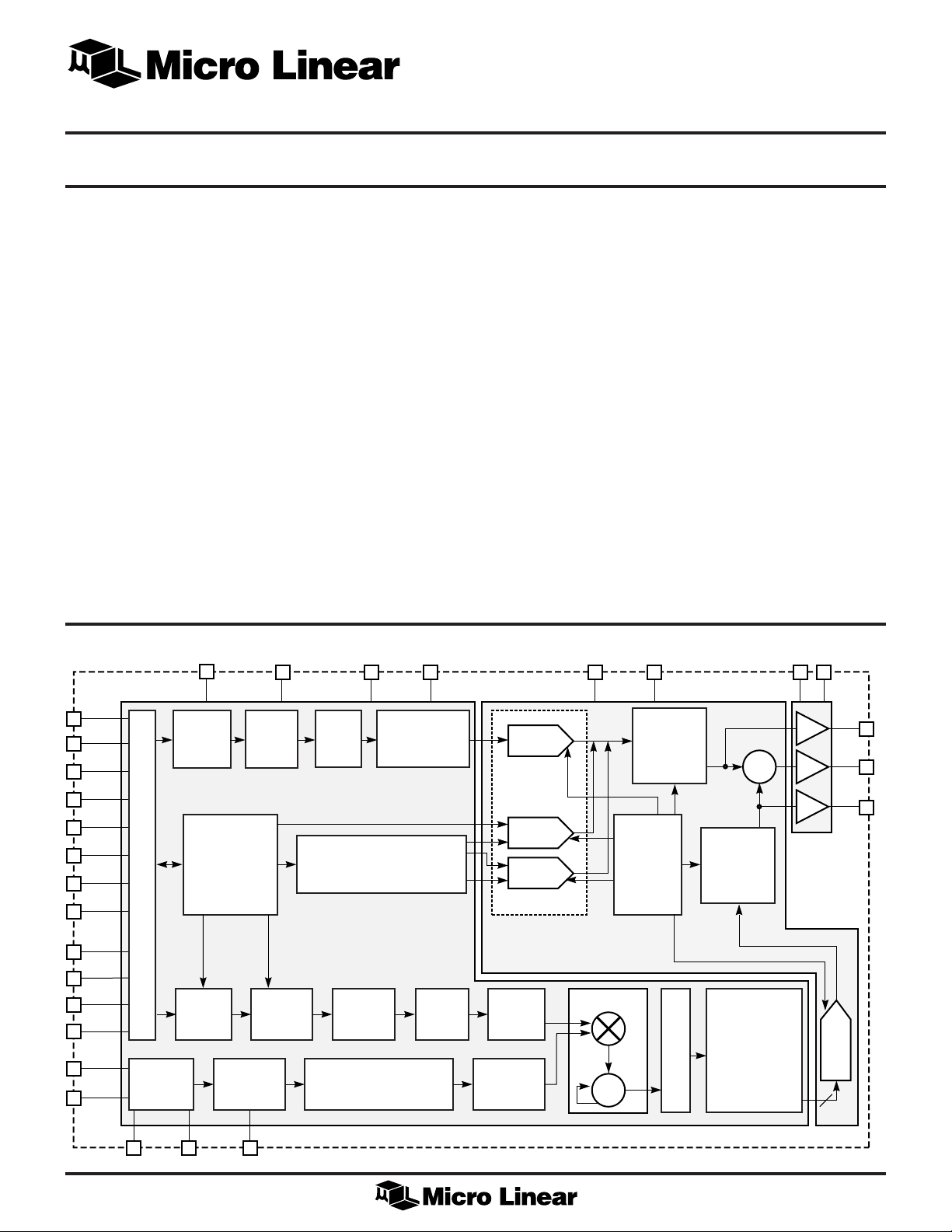
BLOCK DIAGRAM
YCRCB0
21
YCRCB1
20
YCRCB2
19
YCRCB3
18
YCRCB4
17
YCRCB5
13
YCRCB6
12
YCRCB7
11
7
DV
CC1
LUMA
BLANKING
INPUT Y/C DEMUX & CLOCK GENERATOR
TIMING
GENERATOR
(SAV/EAV)
DGNDI
DELAY
COMPEN-
SATION
8
SAMPLER
DV
CC2
UP
CAPTIONING
14
CLOSED
15
DGND2
LUMA
RECONSTRUCTION
FILTER
(FIR)
FEATURES
■ Closed Caption VBI encoder for line 21 and 284
■ Handles SAV/EAV codes for CCIR656 Video
■ Single clock input: 27MHz CCIR656, 24.54MHz Sq. Pix.
■ Color subcarrier correction for overlay applications
■ Onboard analog 7th-order reconstruction filters and
6dB drivers with differential gain/phase of 0.5%/0.5º
■ Y, C, CV outputs drive both AC or DC coupled loads
■ Multiple 75Ω line drivers for two composite outputs,
channel modulator, and S-Video
■ 2-wire serial control bus, or selectable presets for stand-
alone operation
■ Handles Japanese NTSC signals
10 BIT
YDAC
NEGATIVE
SYNC DAC
POSITIVE
SYNC DAC
AV
CC1
1
2
AGND1
7th ORDER
ANALOG
FILTER
WITH
GROUP DELAY
EQUALIZATION
REFERENCE
GENERATOR
+
Σ
+
7th ORDER
ANALOG
FILTER
WITH
GROUP DELAY
EQUALIZATION
AV
CC2
24
25
AGND2
Y
OUT
6dB
6dB
6dB
CV
C
27
OUT
26
OUT
28
16
9
10
5
22
23
CLK
VSYNC
HSYNC
FIELD
SCLK
SDATA
PRESET1
SERIAL
INTERFACE
PRESET0
4
CHROMA
BLANKING
OVERLAY
INTERFACE
PHERR
3 6
BURST
INSERTION
COLOR
SPACE
CONVERTER
PHASE
ACCUMULATOR
UP
SAMPLER
CHROMA
BANDLIMIT
FILTER
SUBCARRIER
GENERATION
MULTIPLYING
ACCUMULATOR
Σ
SAMPLER
UP
CHROMA
RECONSTRUCTION
FILTER
(FIR)
CDAC
8
1
Page 2

ML6461
PIN CONFIGURATION
AV
CC1
AGND1
PRESET0
PRESET1
FIELD
PHERR
DV
CC1
DGND1
VSYNC
HSYNC
YCRCB7
YCRCB6
YCRCB5
DV
CC2
ML6461
28-Pin SOIC (S28)
1
2
3
4
5
6
7
8
9
10
11
12
13
14
TOP VIEW
28
27
26
25
24
23
22
21
20
19
18
17
16
15
C
OUT
Y
OUT
CV
OUT
AV
CC2
AGND2
SDATA
SCLK
YCRCB0
YCRCB1
YCRCB2
YCRCB3
YCRCB4
CLK
DGND2
2
Page 3

PIN DESCRIPTION
ML6461
PIN NAME FUNCTION
1AV
2 AGND1 Analog ground pin
3 PRESET0 Preset input pin for stand alone
4 PRESET1 Preset input pin for stand alone
5 FIELD T his pin can be configured as an input
6 PHERR External chroma lock input
7DV
8 DGND1 Digital ground pin
9 VSYNC Vertical sync hronization signal. Pin is
10 HSYNC Horizontal synchronization signal. Pin
CC1
CC1
Analog 5V supply pin
operation
operation
or output via the control register (bits
B8 and B9). If configured as output, it
can be programmed to give analog or
digital (even/odd) field information. If
configured as input, it can be used to
set analog fields (1 and 2) or (3 and 4).
Digital 5V supply pin
configured as input in external slave
mode and as output in master and
internal slave (CCIR656) modes.
Polarity and function are programmed
in control register in bits B10, B17,
B26, and B28.
is configured as input in external slave
mode and as output in master and
internal slave (CCIR656) modes.
Polarity and function are programmed
in control register in bits B15, B25,
B28, and B29.
PIN NAME FUNCTION
11 YCRCB7 YCRCB digital input bit 7
12 YCRCB6 YCRCB digital input bit 6
13 YCRCB5 YCRCB digital input bit 5
14 DV
15 DGND2 Digital ground pin
16 CLK System clock: 27Mhz (CCIR656 rate),
17 YCRCB4 YCRCB digital input bit 4
18 YCRCB3 YCRCB digital input bit 3
19 YCRCB2 YCRCB digital input bit 2
20 YCRCB1 YCRCB digital input bit 1
21 YCRCB0 YCRCB digital input bit 0
22 SCLK Serial control bus clock input
23 SDATA Serial control bus data input
24 AGND2 Analog ground pin
25 AV
26 CV
27 Y
28 C
CC2
CC2
OUT
OUT
OUT
Digital 5V supply pin
24.54Mhz (Square Pixel rate)
Analog 5V supply pin
Composite video output
Luma output
Chroma output
3
Page 4
ML6461
ABSOLUTE MAXIMUM RATINGS
Absolute maximum ratings are those values beyond which
the device could be permanently damaged. Absolute
Storage Temperature .................................... –65 to 150ºC
Junction T emperature..............................................120ºC
maximum ratings are stress ratings only and functional
device operation is not implied.
OPERATING CONDITIONS
AVCC, DVCC.................................................... –0.3 to 7V
Analog and Digital Inputs/Outputs....–0.3 to AVCC + 0.3V
Input current per pin................................... –25 to 25mA
Temperature Range........................................0°C to 70°C
Operating Supply Range...............................4.5V to 5.5V
ELECTRICAL CHARACTERISTICS
Unless otherwise specified, AVCC = DVCC = 4.5V to 5.5V, TA = Operating Temperature Range (Note 1)
SYMBOL PARAMETER CONDITIONS MIN TYP MAX UNITS
POWER PERFORMANCE
Power Dissipation 750 mW
SUPPLIES
AV
DV
I
I
DIGITAL INPUT SIGNALS
Analog Supply Voltage 4.5 5.5 V
CC
Digital Supply Current 4.5 5.5 V
CC
Analog Supply Current 125 mA
SA
Digital Supply Current Max. Programmed Clock Rates 35 mA
SD
V
V
I
I
DIGITAL OUTPUT SIGNALS
V
V
ENCODER AND DAC (Note 2)
Input Low Voltage 0.8 V
IL
Input High Voltage 2.0 V
IH
Low Level Input Current VIN = at 0.1V 1 µA
IL
High Level Input Current VIN = at DVCC – 0.1V 1 µA
IH
Input Capacitance 2pF
Low Level Output Voltage I
OL
High Level Output Voltage I
OH
Output Capacitance 50 pF
Output Amplitude Accuracy SMPTE Color Bars 2 5 %
CV Output Amplitude SMPTE Color Bars, Peak-to-Peak 0.95 1.05 V
C Output Amplitude SMPTE Color Bars, Peak-to-Peak 0.594 0.657 V
Y Analog/Digital Bandlimit Swept Multiburst 5.7 MHz
C Analog/Digital Bandlimit Swept Multiburst 1.5 MHz
Vector Phase Accuracy (Note 3) Swept Multiburst –2.5 1 2.5 º
Vector Amplitude Accuracy (Note 3) SMPTE Color Bars –2.5 2.5 %
= 2mA 0.4 V
OUT
= 100µA VCC-0.4 V
OUT
Chroma Phase Linearity NTC7 Stepped Subcarrier –2 2 º
Chroma Amplitude Linearity NTC7 Stepped Subcarrier –1 1 IRE
Differential Gain NTC7 Modulated Staircase (Note 2) 0.5 1 %
Differential Phase NTC7 Modulated Staircase (Note 2) 0.5 1 º
4
Page 5
ML6461
ELECTRICAL CHARACTERISTICS (Continued)
SYMBOL PARAMETER CONDITIONS MIN TYP MAX UNITS
ENCODER AND DAC (Continued) (Note 2)
Luma Nonlinearity –1 1 IRE
FSC Phase Jitter (RMS) SMPTE Color Bars 1 º
Quadrature Error SMPTE Color Bars 1 º
SERIAL BUS
SYMBOL PARAMETER CONDITIONS MIN TYP MAX UNITS
INPUT
V
V
I
I
Z
C
Low Level Input Voltage 0 0.8 V
IL
High Level Input Voltage VCC – 0.8 V
IH
Low Level Input Current VIN = 0V 1.0 µA
IL
High Level Input Current VIN = DV
IH
Input Impedance f
IN
Input Capacitance 2pF
IN
SYSTEM TIMING
f
CLOCKSCLK
V
HYS
t
SPIKE
t
WAIT
Input Hysteresis 0.2 V
Spike Suppression Max Length for Zero Response 50 ns
Wait Time From STOP to START
On S
t
HD/START
t
SU/START
t
LOW
t
t
HD/DATA
t
SU/DATA
Hold Time for START On S
Setup Time for START On S
Min LOW Time On S
Min HIGH Time On S
HI
Hold Time On S
Setup Time On Fast mode 100 ns
CC
CC
= 100kHz 1 MΩ
CLK
1.0 µA
V
Frequency 100 kHz
DATA
DATA
CLK
CLK
DATA
DATA
1.3 µs
0.6 µs
1.3 µs
0.6 µs
0.6 µs
5.0 µs
Slow mode 250 ns
t
t
t
SU/STOP
Note 1: Limits are guaranteed by 100% testing, sampling, or correlation with worst case test conditions.
Note 2: All specifications include reconstruction filter and line driver.
Note 3: Normalized to burst.
Rise Time for S
LH
Fall Time for S
HL
Setup Time for STOP On S
CLK
CLK
& S
& S
DATA
DATA
DATA
30 300 ns
30 300 ns
0.6 µs
5
Page 6
ML6461
FUNCTIONAL DESCRIPTION
INTRODUCTION
The ML6461 is a single-chip NTSC video encoder for
generating analog composite (CV) and S-video (Y/C)
outputs from YCrCb digital inputs. The ML6461 is a mixed
signal processor optimizing SNR and distortion by
performing subcarrier generation, sync generation,
modulation and upsampling in the digital domain, while
performing mixing, reconstruction and gain scaling in the
analog domain. In particular , the Y channel requires no
digital scaling, eliminating the need for higher precision
digital solutions. All timing is based on an external clock
source either 27MHz for CCIR656 clock rate or
24.54MHz for square pixel clock rate.
Additionally , the ML6461 allo ws the inclusion of Closed
Captioning codes in the vertical blanking interval (VBI).
Both lines 21 and 284 support Closed Captioning.
DEVICE FUNCTIONAL DESCRIPTION
Video Formats Clock DAC Closed Macrovision Reconstruction 75
Rates Caption Filter Cable
Other special functions include: programmable polarity
and relative position of sync pulses, master and slav e
modes of which includes the ability to handle ITU-R656compliant digital TV or ITU-R/SMPTE specifications,
chroma subcarrier phase and frequency adjustments from
external source; Japanese NTSC support; 100% color bars
processing; and internal 7th order reconstruction filters
with group delay equalization and 6dB line drivers for
direct TV output.
The ML6461 can be programmed and controlled via a
two-wire serial bus or preset modes. A summary of the
features of the ML6461 are listed in Table 1.
VIDEO STANDARDS SUPPORTED
The ML6461 supports NTSC only. The video standards
and clock rates are listed in Table 2.
ΩΩ
Ω
ΩΩ
Encoder Driver
NTSC PAL CCIR656 Square
ML6460 Yes. Input: 8-Bit No Yes Yes Yes. Yes Yes Yes. 7th-order Yes.
YCrCb digital 10-bit Butterworth, with
Outputs: Y , C, DAC group delay
and CV analog equalization
ML6461 Yes. Input: 8-Bit No Yes Yes Yes. Yes No Yes. 7th-order Yes.
YCrCb digital 10-bit Butterworth, with
Outputs: Y , C, DAC group delay
and CV analog equalization
Table 1. Video Encoder Functional Selection
INPUT CLOCK RATE LINES PER FRAME HORIZONTAL LINE
NTSC CCIR656 27 MHz 525 858
NTSC Square Pixel 24.54 MHz 525 780
Table 2: Video Standards and Clock Rates
MODE VSYNC PIN HSYNC PIN FIELD PIN
Master Mode OUT OUT IN/OUT
External Slave Mode IN IN IN/OUT
Internal Slave Mode (SAV/EAV CCIR656) OUT OUT IN/OUT
Pixel
HORIZONTAL PIXELS PER
Table 3: Pin Assignments for Various Master/Slave Modes
6
Page 7

FUNCTIONAL DESCRIPTION (Continued)
ML6461
VIDEO TIMING AND INPUTS
The clock source for the ML6461 can be either 27MHz
(CCIR656) or 24.54MHz (NTSC Square Pixel). The
ML6461 internal timing generator also provides necessary
horizontal and vertical syncs, video blanking, burst, and
closed caption timing. The internal clock is derived
through buffering and inverting the external CLK signal.
The inputs YCRCB<7:0>, VSYNC, and HSYNC are
registered at the rising edge of CLK and PHERR is
registered at the falling edge of CLK. All inputs must be
valid for the minimum setup time of 5ns. The outputs
VSYNC, HSYNC, and FIELD are clocked at the rising edge
of CLK and are valid 10ns following the edge of the clock.
The ML6461 can operate in master and slave modes. In
master mode, the ML6461 internally generates the vertical
reset (VSYNC pin is an output) and horizontal reset
(HSYNC pin is an output). In the slave modes, there are
two alternatives. External sla v e mode allo ws the user to
provide an external vertical reset (VSYNC pin is an input)
and an external horizontal reset (HSYNC pin is an input).
Internal slave mode (CCIR656) uses the SAV and EAV
codes to generate the vertical and horizontal resets. The
master/slave modes are selected via register program.
Table 3 provides a description of the various modes and
the assignments of the VSYNC, HSYNC, and FIELD pins.
MASTER MODE
A logical 0 in the SLAVE/MASTER bit (bit B28) will
configure the ML6461 in the master mode. Multiplexed Y ,
Cr , Cb data is streamed through the YCRCB <7:0> input
pins. VSYNC and HSYNC pins are configured as outputs
and provide vertical and horizontal sync information. The
polarity of the active edge of the HSYNC and VSYNC
pulses can be programmed through the control register via
the SENSE_HSYNC bit (bit B15) and the SENSE_VSYNC
bit (bit B10), respectively. Coincident active edges of the
horizontal and vertical syncs at the start of the line 4
indicates the beginning of an odd field, whereas, the
active edge of the vertical sync pulse when the horizontal
sync is non-active at the middle of line 266, indicates the
beginning of an even field (Figure 1). The FIELD pin can be
configured either as an input or output through the
FRAME_MODE bit (bit B8). If configured as output (B8
=0) it can be set to provide either even/odd field
information (B9 = FLD_FRM_MODE = 0) or analog field
information (B9 = 1). For the former case, a logical 1 on
the FIELD pin indicates odd fields and a logical 0 even
fields. For the latter,(on the FIELD pin), a logical 1 is held
during analog fields 1 and 2, and a logical 0 during analog
fields 3 and 4. If the FIELD pin is configured as an input
(B8 = FRAME_MODE = 1) it must be held low and high on
alternating frames and it should change state at the
beginning of vertical sync during fields 1 and 3. The
internal subcarrier oscillator is reset to make the frame —
for which FIELD pin is held 1 — correspond to analog
fields 1 and 2 (Figure 2). In master mode, a composite
blanking signal is also available thru the HSYNC pin. This
can be activated via the CBLANK bit (B29=1). The
polarity of the composite blanking signal is programmable
from the SENSE_HSYNC bit (B15). When the
SENSE_HSYNC bit is set (B15=1), the ML6461 will output
a logic 0 at the HSYNC pin during the pixels which are
blanked. Conversely, when the SENSE_HSYNC bit is
cleared (B15=0), the ML6461 will output a logic 1 at the
HSYNC pin during the pixels which are blanked.
Consequently, the YCRCB<7:0> inputs will be ignored and
a constant blanking level will be output to the analog
channels YOUT, COUT, and CVOUT. T he operation of the
VSYNC and FIELD pins are not affected by the settings of
CBLANK and SENSE_HSYNC.
SLAVE MODES
A logical 1 in the SLAVE/MASTER bit (B28) will configure
the ML6461 for slave mode. Based on what timing
information is provided, there are two slave modes:
internal and external. Composite blanking—similar to that
described in Master Mode—is also available. Note that in
the internal slave mode, vertical and horizontal sync
pulses and/or composite blanking signals are output for
monitoring purposes only. All timing is derived from SA V/
EAV codes.
Internal Slave Mode for CCIR656 with SAV/EAV codes
In this mode (B26 = SLAVE_MODE=1), all the horizontal
and vertical timing information including odd/even field
selection is embedded in the multiplexed Y, Cr , Cb data
stream input through the YCRCB <7:0> pins. VSYNC and
HSYNC pins are configured as outputs to give vertical and
horizontal sync pulses respectively. The operation of the
FIELD pin is similar to that in the master mode. Composite
blanking — similar to the one described in the master
mode — is also available. Note that in the internal slave
mode, vertical and horizontal sync pulses and / or
composite blanking signal is output for monitoring
purposes only. As mentioned above, all timing is derived
from SAV/EAV codes.
External Slave Mode
In this mode: Where (B26 = SLAVE_MODE=0), horizontal
and vertical reset pulses must be provided externally
through HSYNC and VSYNC pins which are configured as
inputs. The polarity of these pulses is programmed
through bits SENSE_HSYNC (B15) and SENSE_VSYNC
(B10). A horizontal reset pulse on the HSYNC pin can be
given either at the beginning of active video
(B25=HRESET_MODE=1) or at the beginning of horizontal
blanking (B25=HRESET_MODE=0). Once per frame, the
active edge of a vertical reset pulse coincident with the
active edge of a horizontal reset pulse initializes the
internal vertical line counter to the beginning of an odd
field at line 4. Non-coincident vertical reset pulses, for
example, the ones which fall outside of the interval (see
Figure 3) determined by the activ e edge of the horizontal
reset pulse, will be ignored. The FIELD pin, as explained
above can be configured as an input to dictate analog
fields or as an output to monitor odd/even fields or analog
7
Page 8
ML6461
FUNCTIONAL DESCRIPTION (Continued)
fields (1-2) and (3-4). The ML6461 also supports a frame
based synchronization mode (B17 = FSYNC = 1) where a
vertical reset pulse unconditionally resets the vertical line
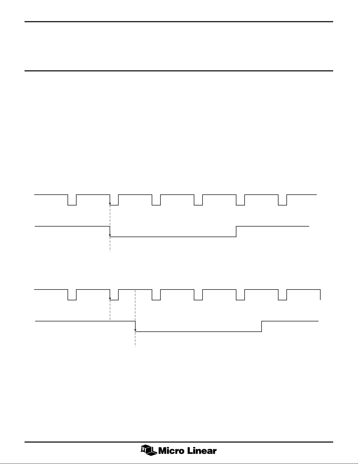
Line 3
HSYNC
Line 4
Coincident
Active Edges
counter to line 4. For proper operation only one acti ve
edge should be sent per frame. The polarity is controlled
by SENSE_VSYNC (B10).
Line 5
Line 6
VSYNC
Beginning of
an Odd Field
HSYNC
VSYNC
Line 265
Line 266
Beginning of
an Even Field
Line 267
Line 268
Line 269
Figure 1. Example of the Beginning of the Odd And Even Fields vs. HSYNC and VSYNC in Master Mode.
(SLAVE/MASTER = 0, SENSE_HSYNC = 0, SENSE_VSYNC
==
= 0)
==
8
Page 9
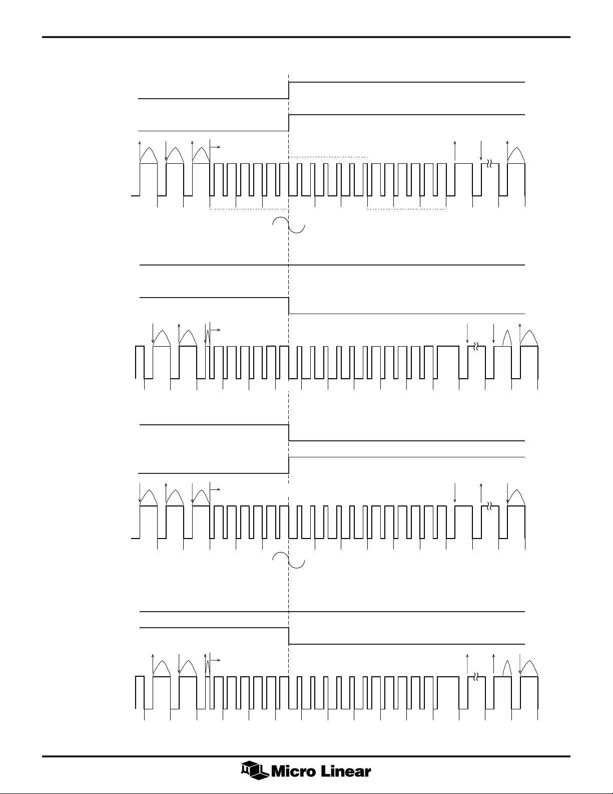
ML6461
FIELD (1,2 and 3,4)
FIELD (ODD/EVEN)
FIELD (1,2 and 3,4)
FIELD (ODD/EVEN)
H
L
H
L
ANALOG
FIELD 1
523 524 525 1 2 3 4 5 6 7 8
EQUALIZING
PULSES
H
L
H
L
ANALOG
FIELD 2
SERRATION
PULSES
BURST PHASE
EQUALIZING
910 22
PULSES
FIELD (1,2 and 3,4)
FIELD (ODD/EVEN)
FIELD (1,2 and 3,4)
FIELD (ODD/EVEN)
261 262 263 264 265 267 268 269 270 271
H
L
H
L
ANALOG
FIELD 3
523 524 525 1 2 3 4 5 6 7 8
H
L
H
L
ANALOG
FIELD 4
266
START
OF VSYNC
BURST PHASE
272 286285
910 22
261 262 263 264 265 267 268 269 270 271
266
Figure 2. Four Fields (M) NTSC Format FIELD Pin Out
272 286285
9
Page 10

ML6461
FUNCTIONAL DESCRIPTION (Continued)
PIXEL SYNCHRONIZATION
Master Mode
In this mode, the active edge of horizontal sync pulse
through the HSYNC pin (configured as an output)
indicates the beginning of an active video line (or the
beginning of the horizontal blanking) and the multiplexed
YCrCb pixel data must be synchronized to this edge for
FIELD (1,2 and 3,4)
FIELD (ODD/EVEN)
H
L
H
L
ANALOG FIELDS 1 & 2
ODD
EVEN
Figure 2a. FIELD Pin Output Summary
proper video location, as well as the proper
demultiplexing of YCrCb values. This synchronization, as
shown in Figures 4 through 5a, is controlled by
SEL_HSYNC1 (B14) and SEL_HSYNC0 (B13). Figures 4
and 4a show synchronization for activ e edge at the
beginning of active video for positive or negative HSYNC
polarity while Figures 5 and 5a show sync hronization for
active edge at the beginning of horizontal blanking for
positive or negative HSYNC polarity.
ANALOG FIELDS 3 & 4 ANALOG FIELDS 1 & 2
ODD
EVEN
ODD
EVEN
HSYNC
VSYNC
HSYNC
VSYNC
active edge of HSYNC
active edge of VSYNC
64 pixels–32 pixels
coincident interval
for HRESET_MODE=0
active edge of HSYNC
active edge of VSYNC
64 pixels
10
coincident interval
for HRESET_MODE=1
Figure 3. Coincident Valid Sync Intervals for External Slave Mode
Page 11

CLK
HSYNC
(output)
ML6461
(0,0) or (0,1) or (1,0) or (1,1) via (SEL_HSYNC1, SEL_HSYNC0)
(0,0) (0,1) (1,0) (1,1)
YCrC
b
CLK
HSYNC
(output)
YCrC
b
BL
BL
BL
BL
BL
Beginning of Active Line
CB0
Y0
T
Selectable Delay Synchronization
CR0
2T
Y1
3T
CB2
Y2
Figure 4. Pixel Synchronization. For Master Mode, Active Edge at Beginning of Active Video.
(CBLANK = 1, SENSE_HSYNC = 0) (BL = Blanked Pixel)
(0,0) or (0,1) or (1,0) or (1,1) via (SEL_HSYNC1, SEL_HSYNC0)
(0,0) (0,1) (1,0) (1,1)
BL
BL
BL
BL
BL
CB0
Y0
CR0
Y1
CB2
Y2
CR2
CR2
Y3
Y3
Beginning of Active Line
T
Selectable Delay Synchronization (SEL_HSYNC1, SEL_HSYNC0)
2T
3T
Figure 4a. Pixel Synchronization. For Master Mode, Active Edge at Beginning of Active Video.
(CBLANK = 1, SENSE_HSYNC = 1) (BL = Blanked Pixel)
11
Page 12

ML6461
CLK
HSYNC
(output)
(0,0) or (0,1) or (1,0) or (1,1) via (SEL_HSYNC1, SEL_HSYNC0)
(0,0) (0,1) (1,0) (1,1)
YCrC
b
Beginning
of Horizontal
Blanking
if ANALOG_HBLANK = 0
if ANALOG_HBLANK = 1
Figure 5. Pixel Synchronization. For Master Mode, Active Edge at Beginning of Horizontal Blanking.
CLK
BL
T2T3T
Q Clock Cycles
# of Clock Cycles, Q
if SELCCIR = 1 if SELCCIR = 0
244 214
252 214
BL
(CBLANK = 0, SENSE_HSYNC = 0) (BL = Blanked Pixel)
BL
BL
BL
BL
CB0
Y0
CR0 Y1
(0,0) or (0,1) or (1,0) or (1,1) via (SEL_HSYNC1, SEL_HSYNC0)
HSYNC (output)
YCrC
b
Beginning
of Horizontal
Blanking
if ANALOG_HBLANK = 0
if ANALOG_HBLANK = 1
(0,0) (0,1) (1,0) (1,1)
BL
T2T3T
Q Clock Cycles
# of Clock Cycles, Q
if SELCCIR = 1 if SELCCIR = 0
244 214
252 214
BL
BL
BL
BL
BL
CB0
Y0
Figure 5a. Pixel Synchronization. For Master Mode, Active Edge at Beginning of Horizontal Blanking.
(CBLANK = 0, SENSE_HSYNC = 1) (BL = Blanked Pixel)
CR0
Y1
12
Page 13

FUNCTIONAL DESCRIPTION (Continued)
ML6461
Internal Slave Mode
Embedded in the YCrCb data stream, the timing code
0xFF, 0x00, 0x00, 0x(SAV) must be inserted before the
samples of the first active pixel. Figures 6 through 6b
illustrate timing for CCIR656 video with SAV and EAV
codes for CCIR or Square Pixel clocking.
External Slave Mode
A horizontal reset pulse can be used either at the beginning
of active video or the beginning of horizontal blanking to
provide synchronization of the YCrCb data to the internal
clock. Bits SEL_HSYNC1(B14) and SEL_HSYNC0 (B13) are
provided to achieve some degree of programmability in this
synchronization. Figures 7 and 7a show synchronization for
active edge at the beginning of active video for positi ve or
negative HSYNC polarity while F igures 8 and 8a sho w
synchronization for active edge at the beginning of
horizontal blanking for positive or negative HSYNC polarity.
Polarity of HSYNC and VSYNC
In both the Master and Slave modes, the HSYNC and
VSYNC polarity can be selected via bit SENSE_HSYNC and
SENSE_VSYNC. When the SENSE_HSYNC bit is set to
logical 1, the HSYNC pulse is on the rising edge. When the
SENSE_HSYNC bit is cleared to logical 0, the HSYNC pulse
is on the falling edge. Similarly, when the SENSE_VSYNC bit
is set logical 1, the VSYNC pulse is on the rising edge.
When the SENSE_VSYNC bit is cleared to logical 0, the
VSYNC pulse is on the falling edge.
HSYNC Timing Delay
In both Master and Slave modes, the SEL_HSYNC1(B14)
and SEL_HSYNC0 (B13) bits of the control register can be
programmed to delay the HSYNC active edge up to three
clock periods, 3T, where T is one period of the clock.
CHROMA AND LUMA PROCESSING
Refer to Figures 9 through 12.
VIDEO OUTPUT STAGE
Reconstruction filtering, clamping, and line drivers
The ML6461 can simultaneously provide outputs for Svideo, two composite video, and a TV modulator.
Differential gain and phase are guaranteed at the outputs
of the line drivers. Two internal 7th-order Butterworth
filters and a group delay equalizer are used as
reconstruction filters on S-video (NTSC). The composite
signal is generated after reconstruction. The S-video (Y and
C) and composite video (CV) are then fed into 75Ω line
drivers.
Each of the filter/drivers are designed to guar antee a
differential phase of 0.5º and differential gain of 0.5%.
01234567 270
0000E
4
Y0
8010801
A
V
0
BLANKING ACTIVE
CR0
Y1
F
F
CB0
In CCIR format, there are
• • • • • • •
268
CB1
CR1
Y2
ACTIVE
720 Y
360 Cb
{}
360 Cr
801
CB2
Y3
in the active portion of a line.
Y4
Figure 6. CCIR Format: CLK = 27MHz
272
FF0000S
0
4
• • • • • • •
1440
274
276
CBYCRY
A
V
278
280
CBYCRY
Y715
282
CB358
Y716
• • • • • • •
1440
CR358
LINE
Y717
CB359
LINE
Y718
1711
Y
1713
Y
C
B
CR359
1715
CRY
Y719
13
Page 14

ML6461
01234567 276
0000E
4
Y0
8010801
A
V
0
BLANKING ACTIVE LINE
CR0
Y1
F
F
CB0
In SQPIX format, there are
• • • • • • •
272
CB1
CR1
Y2
ACTIVE
640 Y
320 Cb
{ }
320 Cr
801
• • • • • • •
in the active portion of a line.
Figure 6a. Square Pixel (SQPIX) Format: CLK = 24.54MHz
278
FF0000S
0
Y634
1280
280
4
A
V
CR317
282
284
CBYCRY
Y635
286
CBYCRY
CB318
288
Y636
CR318
LINE
• • • • • • •
1280
Y637
CB319
Y638
1555
Y
1557
C
B
CR319
Y
1559
CRY
Y639
EAV and SAV Code Format (8-bits)
1 F V H P3 P2 P1 P0
SYNCHRONIZATION
BITS
Format <1,F,V,H,P3,P2,P1,P0>
Line Number Code 1 F V H P3~P0
1 to 3 EAV 1 1 1 1 X
SAV 1 1 1 0 X
4 to 19 EAV 1 0 1 1 X
SAV 1 0 1 0 X
20 to 263 EAV 1 0 0 1 X
SAV 1 0 0 0 X
264 to 265 EAV 1 0 1 1 X
SAV 10 10 X
266 to 282 EAV 1 1 1 1 X
SAV 1 1 1 0 X
283 to 525 EAV 1 1 0 1 X
SAV 1 1 0 0 X
PROTECTION BITS
(IGNORED BY ML6461)
Figure 6b. SAV/EAV Codes for 525/60.
14
Page 15

CLK
HSYNC
(input)
ML6461
YCrC
b
BL
BL
Beginning of
Active Line
A
B
Selectable Delay Synchronization (SEL_HSYNC1, SEL_HSYNC0)
Bit
C
A
B
C
D
E
F
G
H
D
Value (SEL_HSYNC1, SEL_HSYNC0)
(0,0)
CB0
Y0
CR0
Y1
CB2
Y2
CR2
Y3
E
(0,1)
BL
CB0
Y0
CR0
Y1
CB2
Y2
CR2
F
(1,0)
BL
BL
CB0
Y0
CR0
Y1
CB2
Y2
Figure 7. Pixel Synchronization. For External Mode, Active Edge at Beginning of Active Video.
(HRESET_MODE = 1, SENSE_HSYNC = 0, BL = Blanked Pixel)
(ANALOG_HRESET = ANALOG_HBLANK = 0 OR ANALOG_HRESET = ANALOG_HBLANK = 1)
GH
(1,1)
BL
BL
BL
CB0
Y0
CR0
Y1
CB2
CLK
HSYNC
(input)
YCrC
b
BL
BL
Beginning of
Active Line
A
B
Selectable Delay Synchronization (SEL_HSYNC1, SEL_HSYNC0)
Bit
C
A
B
C
D
E
F
G
H
D
Value (SEL_HSYNC1, SEL_HSYNC0)
(0,0)
CB0
Y0
CR0
Y1
CB2
Y2
CR2
Y3
E
(0,1)
BL
CB0
Y0
CR0
Y1
CB2
Y2
CR2
F
(1,0)
BL
BL
CB0
Y0
CR0
Y1
CB2
Y2
Figure 7a. Pixel Synchronization. For External Mode, Active Edge at Beginning of Active Video.
(HRESET_MODE = 1, SENSE_HSYNC = 1, BL = Blanked Pixel)
(ANALOG_HRESET = ANALOG_HBLANK = 0 OR ANALOG_HRESET = ANALOG_HBLANK = 1)
GH
(1,1)
BL
BL
BL
CB0
Y0
CR0
Y1
CB2
15
Page 16

ML6461
CLK
HSYNC
(input)
YCrC
b
Beginning
of Horizontal
Blanking
If ANALOG_HBLANK = 0
If ANALOG_HBLANK = 1
BL
P Clock Cycles
# of Clock Cycles, P
if SELCCIR = 1 if SELCCIR = 0
244 220
252 220
BL
A
B
Selectable Delay Synchronization (SEL_HSYNC1, SEL_HSYNC0)
Bit
C
A
B
C
D
E
F
G
H
D
Value (SEL_HSYNC1, SEL_HSYNC0)
(0,0)
CB0
Y0
CR0
Y1
CB2
Y2
CR2
Y3
E
(0,1)
BL
CB0
Y0
CR0
Y1
CB2
Y2
CR2
F
(1,0)
BL
BL
CB0
Y0
CR0
Y1
CB2
Y2
(1,1)
CB0
CR0
CB2
Figure 8. Pixel Synchronization. For External Mode, Active Edge at Beginning of Horizontal Blanking.
(HRESET_MODE = 0, SENSE_HSYNC = 0, BL = Blanked Pixel)
GH
BL
BL
BL
Y0
Y1
CLK
HSYNC
(input)
YCrC
b
Beginning
of Horizontal
Blanking
If ANALOG_HBLANK = 0
If ANALOG_HBLANK = 1
BL
P Clock Cycles
# of Clock Cycles, P
if SELCCIR = 1 if SELCCIR = 0
244 220
252 220
BL
A
B
Selectable Delay Synchronization (SEL_HSYNC1, SEL_HSYNC0)
Bit
C
A
B
C
D
E
F
G
H
D
Value (SEL_HSYNC1, SEL_HSYNC0)
(0,0)
CB0
Y0
CR0
Y1
CB2
Y2
CR2
Y3
E
(0,1)
BL
CB0
Y0
CR0
Y1
CB2
Y2
CR2
F
(1,0)
BL
BL
CB0
Y0
CR0
Y1
CB2
Y2
GH
(1,1)
BL
BL
BL
CB0
Y0
CR0
Y1
CB2
Figure 8a. Pixel Synchronization. For External Mode, Active Edge at Beginning of Horizontal Blanking.
(HRESET_MODE = 0, SENSE_HSYNC = 1, BL = Blanked Pixel)
16
Page 17

ML6461
10
0
–10
–20
(dB)
–30
–40
–50
–60
13 64
02 7
INPUT FREQUENCY (MHz)
5
(dB)
1
0
–1
–2
–3
–4
0.25
0
INPUT FREQUENCY (MHz)
1.751.250.75
1.5120.5
Figure 9. Chroma Bandlimit Filter: Stopband (FIR Filter) Figure 10. Chroma Bandlimit Filter: Passband (FIR Filter)
ANALOG RECONSTRUCTION FILTER
DIGITAL FIR FILTER
TOTAL FILTER AND BUFFER RESPONSE
10
0
–10
–20
(dB)
–30
–40
–50
–60
515 3020
110 25
INPUT FREQUENCY (MHz)
TOTAL FILTER AND BUFFER RESPONSE
1
0
–1
–2
(dB)
–3
–4
–5
–6
13 64
02 7
INPUT FREQUENCY (MHz)
DIGITAL FIR FILTER
5
Figure 11. Reconstruction Filter: Stopband (Normalized) Figure 12. Reconstruction Filter: Passband (Normalized)
17
Page 18

ML6461
FUNCTIONAL DESCRIPTION (Continued)
PHASE ERROR INPUT AND CHROMA SUBCARRIER
CORRECTION (FOR OVERLAY APPLICATIONS)
The chroma oscillator phase and frequency can be altered
in real time using the PHERR input. This pin can receive a
signal that corrects chroma variations for signals with
unstable time base errors. T o properly initialize the ML6461
overlay interface, follow the steps belo w:
1. Set the control register bit OVERLAY_ON (B16) to logical
0. T his will disable the interface and let the c hroma
subcarrier oscillator run free.
2. Force the PHERR input to logical 0 (idle state) for at least
128 clock cycles and set the control register bit
OVERLAY_ON (B16) to logical 1 while PHERR is held
low . This will enable the interface.
3. Clock in the startup code of 101 and then serially (LSB
first) the 32-bit frequency value FSQ (frequenc y number)
followed by the 12-bit phase value PHQ (phase number).
Equation 1 calculates color subcarrier frequency:
F
F
SQ
=×
F
SC
Where F
clock and FSC is the actual color subcarrier frequency.
CLK
32
2
2
is the 27 MHz (or 24.54MHz) as the system
CLK
(1)
4. Repeat STEP 2 as many times as needed.
Note that CC data is transmitted once (twice if both lines
are used) per frame. Hence attempts to transmit CC data
at a rate faster than four bytes per frame will result on
overwriting some of the previously entered data before the
encoder has a chance to transmit. To prevent ov erwriting
of data, the CC controller and the ML6461 need to be
synchronized. This can be easily achieved by polling the
vertical blanking pulse and updating the CC data registers
once per frame during the vertical blanking interval or any
appropriate interval which does not include lines 21 or
284. Also, activ e video information is blanked on lines for
which closed caption transmission is enabled. Note that
the last data written on the CC registers will be sent
continuously once per frame (on line 21 or line 284
depending on the mode chosen) until the interface is
disabled. Figure 13 shows Closed Caption wa v eforms for
various modes. See Table 7 and F igure 17 for more Closed
Caption information. Note that parity bits A7, A15, A23,
and A31 must be generated externally.
PROGRAMMING INTERFACE
The ML6461 can be programmed either through PRESET
modes or through SERIAL BUS mode.
REGISTER INFORMATION
4. To turn-off the interface and have the subcarrier oscillator
on free run, the control register bit OVERLAY_ON (B16)
must be reset to logical 0.
5. When this function is disabled, the internal default values
for FSQ are:
0X 43E0F7AD for CCIR656
0X 4AAAAA0B for Square Pixel.
CLOSED CAPTIONING
The ML6461 enables the transmission of VBI Closed
Caption codes on lines 21 and 284. To properly initialize
the closed caption interface, follow the steps below:
1. Set the control register bits CC_21 (B19) and CC_284
(B18) to logical 0. This will disable transmission of
Closed Caption (CC) data.
2. F or each line, write the two byte closed caption (CC)
data, including the parity bit, to the CC data register
through the serial bus interface. Note that the ML6461
does not generate the parity bits. If only line 21 or line
284 transmission is desired, only two bytes of data are
needed per frame. If both lines are used for
transmission, then four bytes (the first two bytes
corresponding to line 21) must be entered all at once
into the closed caption data register (CC register).
3. Set the control register bits CC_21 (B19) and/or CC_284
(B18) to logical 1. This will enable CC transmission at
the desired lines.
See Table 6 for ML6461 register summary information.
CONTROL REGISTERS: DESCRIPTION OF FUNCTION
Reserved, B31:B30 These bits are reserved and must be
set to 1 (B31=B30=1) for normal operation.
CBLANK, B29 In master mode, and internal slave mode,
a composite blanking signal is also available thru the
HSYNC pin. This can be activated via the CBLANK bit
(B29=1). T he polarity of the composite blanking signal is
programmable thru the SENSE_HSYNC bit (B15). When
the SENSE_HSYNC bit is set (B15=1), the ML6461 will
output a logic 0 at the HSYNC pin during the pixels
which are blanked. Conversely, when the
SENSE_HSYNC bit is cleared (B15=0), the ML6461 will
output a logic 1 at the HSYNC pin during the pixels
which are blanked. Consequently, the YCRCB<7:0>
inputs will be ignored and a constant blanking level will
be output to the analog channels YOUT, COUT , and
CVOUT. T he oper ation of the VSYNC and FIELD pins are
not affected by the settings of CBLANK and
SENSE_HSYNC.
SLAVE/MASTER, B28 T his bit determines if device
operates in master or slave modes. Configuration of
HSYNC, VSYNC and FIELD are determined upon
selection of this bit. Table 3 provides a summary of Slave /
Master modes. When this bit is set (B28=1), the ML6461
is in slave mode. When this bit is cleared (B28=0), the
ML6461 is in master mode. Special note for slave modes:
this bit (B28) along with the SLAVE_MODE bit (B26)
18
Page 19

FUNCTIONAL DESCRIPTION (Continued)
ML6461
selects between internal (B26=1) and external slave
modes (B26=0).
SELCCIR, B27 This bit determines the frequency of
choice between CCIR656 clock rate(27MHz) and Square
Pixel clock rate (24.54MHz). When this bit is set (B27=1),
CCIR656 clock rate is selected. When this bit is cleared
(B27=0), the Square Pixel clock rate is selected.
SLAVE_MODE, B26 This bit determines the choice of
two slave modes: internal sla ve mode or external slave
mode. In internal slave mode (B26=1), horizontal and
vertical timing information is embedded in the YCrCb
data (via SAV / EAV codes); while the HSYNC and
VSYNC pins can be used as outputs. In external slave
mode (B26=0), horizontal and vertical sync pulses must
12.91µs
7 CYCLES
TWO: 7 BIT + PARITY BIT
S
T
A
R
T
A0 ~ A6
A7
LINE 21
A8 ~ A14
A15
50 ±2 IRE
BLANK
LEVEL
40 IRE
10.5
±0.25µs
3.58MHz
COLOR
BURST
be provided for timing and synchronization;in this case
HSYNC and VSYNC pins are inputs. See T able 3.
HRESET_MODE, B25 This bit determines whether the
HSYNC is given at the beginning of active video (B25=1)
or HSYNC is given at the beginning of blanking (B25=0).
This bit (B25) is only a v ailable for external sla ve modes.
ANALOG_HBLANK, B24 This bit determines whether
the ML6461 is to encode for ITU_R656_compliant
"digital" or ITU_/SMPTE_compliant "analog" encoding
specifications. When this bit is cleared (B24=0), the
ML6461 is optimized for full "digital" line encoding,
where the number of active pixels is 720 for CCIR656
rates and 640 for square pixel rates. No tapering (edge
12.91µs
7 CYCLES
TWO: 7 BIT + PARITY BIT
S
T
A
R
T
A0 ~ A6
A7
LINE 284
A8 ~ A14
50 ±2 IRE
BLANK
LEVEL
40 IRE
10.5
±0.25µs
3.58MHz
COLOR
BURST
A15
SYNC
LEVEL
50 ±2 IRE
BLANK
LEVEL
SYNC
LEVEL
10.003
±0.25µs
27.382µs
Closed Caption on Line21
[CC_21 = 1 and CC_284 = 0]
10.5
±0.25µs
3.58MHz
COLOR
BURST
40 IRE
10.003
±0.25µs
12.91µs
7 CYCLES
27.382µs
33.764µs
TWO: 7 BIT + PARITY BIT
S
T
A
R
T
A0 ~ A6
A7
LINE 21
33.764µs
A8 ~ A14
A15
SYNC
LEVEL
50 ±2 IRE
BLANK
LEVEL
40 IRE
SYNC
LEVEL
10.003
±0.25µs
27.382µs
Closed Caption on Line284
[CC_21 = 0 and CC_284 = 1]
7 CYCLES
27.382µs
12.91µs
TWO: 7 BIT + PARITY BIT
S
T
A16 ~ A22
A
R
T
10.5
±0.25µs
3.58MHz
COLOR
BURST
10.003
±0.25µs
33.764µs
A23
LINE 284
33.764µs
A24 ~ A30
A31
Closed Caption on Line21 and Line 284
[CC_21 = 1 and CC_284 = 1]
Figure 13. Closed Caption on Line 21 and Line 284.
19
Page 20

ML6461
FUNCTIONAL DESCRIPTION (Continued)
smoothing) is done to the beginning and end of the active
portion of the line. When this bit is set (B24=1), the
ML6461 is optimized for "analog" line encoding, where
the number of active pixels is 712 for CCIR656 rates and
640 for square pixel rates. The beginning and end of the
active video portion of the line is tapered (smoothed) to
minimize ringing introduced due to fast transitions. Figure
14 below illustrates the timing comparisons.
Note: For the square pixel rate the only difference
between "analog" and "digital" encoding is the tapering
(smoothing) at the beginning and end of the active video
portion of the line. T he number of pixels encoded during
the active video portion is the same in both cases. The
positioning of the active portion is the same as in "analog"
line encoding.
ANALOG_HRESET, B23 This bit is acti v e only in
external slave mode and when the external sync is gi v en
at the beginning of active video. In this mode,
ANALOG_HRESET (B23) must be used in conjunction
with ANALOG_HBLANK (B23) to choose between
"analog" and digital" line encoding. T he possible
approaches are summarized in Table 4 below.
FULL_BAR, B22 This bit is used to program the ML6461
to encode in normal modes or 100% amplitude video
(100% color bar). When this bit is set (B22=1), the
ML6461 is ready to handle 100% color bars. W ith 75%
amplitude signals, this bit should be cleared (B22=0) for
optimum signal to noise performance.
JAPAN_BLANK, B21 This bit is used to program the
ML6461 to encode Japanese NTSC by removing the 7.5
IRE setup in blanking and thus boosting the gain of luma
and chroma D A Cs. This bit is set (B21=1) to handle
Japanese NTSC modes.
WIDE_VBLANK, B20 Determines which lines to blank
at the beginning of each field. For wide blanking, this bit
is set (B20=1), the ML6461 provides 15 lines of blanking.
For narrow blanking, this bit is cleared (B20=0), the
ML6461 provides 9 lines of blanking.
CC_21, B19 T his bit enables (B19=1) and disables
(B19=0) the transmission of closed captioning data on
line 21.
5.3µs 9 CYCLES
4.7µs
CCIR656 DIGITAL LINE ENCODING: 720 PIXELS, 1440 TCLKs
1.56µs
9µs
9µs + 4 PIXELS
CCIR656 ANALOG LINE ENCODING: 712 PIXELS, 1424 TCLKs
SQUARE PIXEL ANALOG AND
DIGITAL ENCODING: 640 PIXELS, 1280 TCLKs
Figure 14. Timing of Horizontal Blanking Interval and Active Video
ANALOG_ ANALOG_ RECOMMENDED TIME BETWEEN PIXELS EDGE
HRESET HBLANK ENCODING H_SYNC AND ENCODED SMOOTHING
B23 B24 ACTIVE VIDEO CCIR 656 SQUARE PIXEL (B24 = 1)
0 0 ITU-R656 9µs 720 640 none
Digital TV Line
0 1 Optional 9µs + 4pixels 712 640 Yes
= 9.3µs See Note 1
1 0 Not
Recommended
1 1 ITU-R/SMPTE 9µs + 4pixels 712 64 0 Y es
Analog = 9.3µs See Note 2
Note 1: Ignore first four and last four pixels.
Note 2: Ignore last eight pixels.
Table 4. Video Encoding Standards and Horizontal/Active Video Timing
20
Page 21

FUNCTIONAL DESCRIPTION (Continued)
ML6461
CC_284, B18 This bit enables (B18=1) and disables
(B18=0) the transmission of closed caption data on line
284.
FSYNC, B17 T his bit enables (B17=1) and disables
(B17=0) frame syncing.
OVERLAY_ON, B16 T his bit enables (B16=1) and
disables (B17=0) the PHERR pin to be used as an
interface to set the internal subcarrier oscillator’ s phase
and frequency.
SENSE_HSYNC, B15 This bit selects the polarity of the
HSYNC active edge to a rising edge (if B15=1) or a falling
edge (if B15=0). T his bit is acti v e in master modes or in
external slave modes. In internal sla v e modes HSYNC is
configured as an output to be used for monitoring
purposes. T he polarity is still affected b y this bit.
SEL_HSYNC1, B14 This bit, in conjunction with
SEL_HSYNC0 (B13), is used to facilitate pixel
synchronization. Figures 4, 5, 7, and 8 provide a detailed
description. This bit is only active in master modes or in
external slave modes. This bit is de-activated in internal
slave modes.
SEL_HSYNC0, B13 This bit, in conjunction with
SEL_HSYNC1 (B14), is used to facilitate pixel
synchronization. Figures Figures 4, 5, 7, and 8 pro vide a
detailed description. T his bit is only acti ve in master
modes or in external slave modes. This bit is de-activated
in internal slave modes.
SWITCH_UV, B12 This bit is used to switch Cr and Cb
internally when set (B12=1). This bit is cleared (B12=0)
for normal operation. T his bit is intended for debug
purposes only . If used, there may be some slight artifacts
at the end of active line.
SWITCH_FIELD, B11 This bit is used to switch even/odd
fields when set (B11=1). T his bit is cleared (B12=0) for
normal operation. This bit is only active in internal slave
mode.
SENSE_VSYNC, B10 This bit selects the polarity of the
VSYNC active edge to a rising edge (if B10=1) or a falling
edge (if B10=0). In internal slave modes VSYNC is
configured as an output to be used for monitoring
purposes. T he polarity is still affected b y this bit.
FLD_FRM_MODE, B9 When set (B9=1), it causes the
ML6461 FIELD pin to give analog field information if the
FIELD pin is configured as an output (see B8). When
cleared (B9=0), it causes the field pin to give odd/even
field information if the FIELD pin is configured as an
output (see B8).
FRAME_MODE, B8 T his bit configures the FIELD pin of
the ML6461 as an input (if B8=1) or as an output (if
B8=0).
YDEL1, B7 This bit, in conjunction with YDEL0 (B6), is
used to select luma delay in order to align luma and
chroma data. See Table 5.
YDEL0, B6 This bit, in conjunction with YDEL1 (B7), is
used to select luma delay in order to align luma and
chroma data. See Table 5.
BURST_ON, B5 When active (B5=1) this bit provides
burst at all times for testing purposes only . For normal
operation this bit is cleared (B5=0).
ACTIVE_ON, B4 When acti v e (B4=1) this bit eliminates
horizontal and vertical blanking intervals. Burst is
suppressed. For testing purposes only. For normal
operation this bit is cleared (B4=0).
FIX_SCH, B3 When activ e (B3=1) this bit maintains SCH
phase. In this condition known as a “coherent
subcarrier” such that the subcarrier has a known phase
relative to the activ e edge of HSYNC pulse. When this
bit is cleared (B3=0), the subcarrier generation block is in
free run mode. T his condition is known as “incoherent
subcarrier” where the phase of the subcarrier relative to
the HSYNC is not fixed.
CC_ALL, B2 When active (B2=1) this bit enables closed
caption transmission on every line. For testing purposes
only . For normal operation this bit is cleared (B2=0) and
closed caption is enabled through control register bits
CC_21 (B19) and CC_284 (B18).
SUBCARRIER_OFF, B1 When active (B1=1) this bit
disables the internal subcarrier oscillator . Used for test
purposes only . For normal operation this bit is cleared
(B1=0).
AC_DC, B0 This bit configures the output buffers for A C
coupled drive (if B0=1) and DC couple drive (if B0=0).
YDEL1 YDEL0 OPERATION
(B7) (B6)
0 0 Normal
0 1 Delay Luma Channel by 1 TCLK
1 0 Advance Luma Channel by 1 TCLK
1 1 Advance Luma Channel by 2 TCLK
Table 5. Luma Delay Selection
21
Page 22

ML6461
DATA BIT NAME DESCRIPTION BIT CODE RANGE
B0 AC_DC Configures analog output buffers for AC or DC drive 0 = DC, 1 = AC
B1 SUBCARRIER_OFF Disable internal subcarrier oscillator - for test only 0 = Normal, 1= Disable oscillator
B2 CC_ALL Enables Closed Caption transmission on every line 0 = Normal, 1 = Enable
B3 FIX_SCH Enable reset of subcarrier oscillator every other frame 0 = Not reset, 1 = Oscillator reset
to maintain SCH phase
B4 ACTIVE_ON Eliminate H & V intervals, suppress burst — for test only 0 = Normal, 1 = Test Mode
B5 BURST ON Burst Available at all time — For test only 0 = Normal, 1 = Test Mode
B6 YDEL0 Delay/Advance luma channel <YDEL1, YDEL0> = 00 = Normal
<YDEL1, YDEL0> = 01= Delay luma 1 clock cycle
B7 YDEL1 Delay/Advance luma channel <YDEL1, YDEL0> = 10 = Advance luma 1 clock cycle,
<YDEL1, YDEL0> = 11= Advance luma 2 clock cycles
B8 FRAME_MODE Configure FIELD pin as input or output 0 = output, 1= input
B9 FLD_FRM_MODE Configure FIELD pin to give odd/even or 1,2 and 3,4 info 0 = odd/even, 1= 1,2 or 3,4
B10 SENSE_VSYNC Set vertical reset pulse polarity 0 = Falling edge, 1= Rising edge
B11 SWITCH_FIELD Switches even/odd fields 0 = Normal, 1= switch even/odd
B12 SWITCH_UV Switch Cr and Cb internally 0 = Normal, 1= Switch Cr & Cb
B13 SEL_HSYNC0 Used to facilitate pixel synchronization See Figures 4, 5, 7, 8
B14 SEL_HSYNC1 Used to facilitate pixel synchronization See Figures 4, 5, 7, 8
B15 SENSE_HSYNC Set horizontal reset pulse polarity 0 = Falling edge, 1= Rising edge
B16 OVERLAY_ON Enables use of PHERR pin 0 = Disable, 1= Enable PHERR pin
B17 FSYNC Enable frame syncing 0 = Disable, 1= Enable
B18 CC_284 Enable transmission of Closed Caption data on line 284 0 = Disable, 1= Enable transmission
B19 CC_21 Enable transmission of Closed Caption data on line 21 0 = Disable, 1= Enable transmission
B20 WIDE_BLANK Select wide or narrow blanking 0 = 9 lines of blanking, 1= 15 lines
B21 JAPAN_BLANK Removes 7.5 IRE setup in blanking and boosts Y & C gain 0 = Normal, 1= Japanese NTSC
B22 FULL_BAR To handle 100% amplitude video (100% colorbars) 0 = Normal, 1 handles 100%Amp. Video
B23 ANALOG_HRESET Selects position of horizontal reset 0 = Digital H blank edge,
1= Analog H blank edge
B24 ANALOG_HBLANK Select analog blanking with smooth transition at the edges 0 = Digital blanking,
or digital blanking 1= Analog blanking
B25 HRESET_MODE Select H reset at start of active video or start of H blanking 0 = Start of blanking,
1= Start of active
B26 SLAVE_MODE Select external H/V reset or embedded H/V reset
0=External H/V reset (H/V ext. source)
1=Embedded H/V reset (SAV/EAV codes)
B27 SELCCIR Select CCIR656 rate or Square Pixel rate 0 = Square Pixel, 1= CCIR656
B28 SLAVE/MASTER Select slave or master mode 0 = Master mode, 1= Slave mode
B29 CBLANK Composite Blanking 0 = Disable, 1= Enable
B30 Reserved Set to 1 for Proper Operation
UPPER BYTE UPPER MIDDLE BYTE LOWER MIDDLE BYTE LOWER BYTE
B31 Reserved Set to1 for Proper Operation
Note: B31 is MSB
Table 6: Control Register (CNTR) Summary
22
Page 23

ML6461
DATA BIT NAME DESCRIPTION CC-21=1; CC-284=0 CC21=0; CC-284=1 CC21=1; CC-284=1
A0 CC0 Closed Caption bit 0 line 21 line 284 line 21
A1 CC1 Closed Caption bit 1 line 21 line 284 line 21
A2 CC2 Closed Caption bit 2 line 21 line 284 line 21
A3 CC3 Closed Caption bit 3 line 21 line 284 line 21
A4 CC4 Closed Caption bit 4 line 21 line 284 line 21
A5 CC5 Closed Caption bit 5 line 21 line 284 line 21
A6 CC6 Closed Caption bit 6 line 21 line 284 line 21
A7 CC7 Closed Caption bit 7 line 21 line 284 line 21
A8 CC8 Closed Caption bit 8 line 21 line 284 line 21
A9 CC9 Closed Caption bit 9 line 21 line 284 line 21
A10 CC10 Closed Caption bit 10 line 21 line 284 line 21
A11 CC11 Closed Caption bit 11 line 21 line 284 line 21
A12 CC12 Closed Caption bit 12 line 21 line 284 line 21
A13 CC13 Closed Caption bit 13 line 21 line 284 line 21
A14 CC14 Closed Caption bit 14 line 21 line 284 line 21
A15 CC15 Closed Caption bit 15 line 21 line 284 line 21
A16 CC16 Closed Caption bit 0 X X line 284
A17 CC17 Closed Caption bit 1 X X line 284
A18 CC18 Closed Caption bit 2 X X line 284
A19 CC19 Closed Caption bit 3 X X line 284
A20 CC20 Closed Caption bit 4 X X line 284
A21 CC21 Closed Caption bit 5 X X line 284
A22 CC22 Closed Caption bit 6 X X line 284
A23 CC23 Closed Caption bit 7 X X line 284
A24 CC24 Closed Caption bit 8 X X line 284
A25 CC25 Closed Caption bit 9 X X line 284
A26 CC26 Closed Caption bit 10 X X line 284
A27 CC27 Closed Caption bit 11 X X line 284
A28 CC28 Closed Caption bit 12 X X line 284
A29 CC29 Closed Caption bit 13 X X line 284
A30 CC30 Closed Caption bit 14 X X line 284
A31 CC31 Closed Caption bit 15 X X line 284
UPPER BYTE UPPER MIDDLE BYTE LOWER MIDDLE BYTE LOWER BYTE
Note: A31 is MSB
Table 7. Closed Caption (CC) Register Summary
23
Page 24

ML6461
FUNCTIONAL DESCRIPTION (Continued)
PRESET PIN CONTROL
The ML6461 can be controlled by a pair of preset mode
pins. These pins do not allow access to all of the
programmable features of the ML6461, but are intended to
provide a simpler interface for most applications. Refer to
Table 8 for preset modes.
SERIAL BUS OPERATION
The serial bus control in the ML6461 has two lev els of
addressing: Device Addressing and Functional Addressing.
Device Addressing: Figures 15, 16, and 17 show the
physical waveforms generated in order to address the
ML6461. There are six basic parts of the waveform:
1. Start Indication: Clock Cycle 0
2. Device Address Shifted in: Clock Cycle 1 through 8
3. Device Address Strobed and Decoded: Clock Cycle 9
4. Function Address Shifted in: Cloc k Cycle 10 through 17
5. Function Address Strobed and Decoded: Clock Cycle 18
6. Data Shifted in 8 bits at a time, MSB first: Clock
Cycle 19 through 26
7. Data Shifted: Clock Cycle 27
8. Repeat strep 6 & 7 until all data is clocked in.
9. Stop indication: After Last Clock Cycle
(54 for CC, 54 for CNTR)
Device Address (8 bit)
1011 0100 (Hex = B4)
Function Address (8 bit)
Closed Caption Data Registers (CC): 0000 0000
Control Registers (CNTR): 0000 0011
Number of Data Bits
Closed Caption Data Registers (CC): 4 x 8 bits
Control Registers (CNTR): 4 x 8 bits
CONTROL REGISTER DEFAULT SETTINGS
At Power up, the ML6461 default settings are as follo ws:
• Control Register is undefined when the serial
bus mode is enabled.
• Chip is ready to process video
• Preset Pins are available and if used will
configure the control register .
• Must write logic “0” (zero) to A30 to get
video
To get black at power up will require logic “1” in A30.
(Hex =
(Hex =
03)
00)
Note: data at SDATA is ignored at steps 3, 5, and 7.
Device & Function Addressing: Figures 15, 16, an17
show the register address procedure of the ML6461.
MODE PRESET1 PRESET0 CC CNTR
A 0 0 XX XXXXXXXX
B 0 1 XX 09080209
C 1 0 XX 1C080209
D 1 1 XX 11080209
X = don't care
Mode Description
Mode A: All register contents are programmed through serial interface.
Mode B: Master mode, CCIR656 rate, analog blanking.
Mode C: Slave mode, SAV and EAV codes, CCIR656 rate, digital blanking.
Mode D: Slave mode, external sync at start of line, Square pixel rate, analog blanking
24
Table 8. Preset Modes and Register Values
Page 25

S
ML6461
START
DATA
t
RISE
t
SET/START
S
CLK
START: A Falling Edge on the S
STOP: A Rising Edge on the S
DATA
DATA
While S
While S
is Held High
CLK
is Held High
CLK
All Other S
Transitions Must Occur While S
DATA
CLK
is Low
Figure 15. Definition of START & STOP on Serial Data Bus
t
FALL
STOP
START
S
DATA
S
CLK
DEVICE ADDRESS FUNCTION ADDRESS
MSB
A1 A0A6A7
0
1 2 7 8 9 10 11 16 17 18
9th pulse strobes dummy bit for ACK
S
:
CLK
Rising edge enables data transfer
S
:
CLK
Value set to A6, Device Address (MSB-1)
S
:
DATA
Falling edge disables data transfer
S
:
CLK
Rising edge enables data transfer
S
:
CLK
Value set to A7, Device Address MSB
S
:
DATA
Falling edge in prep for first address transfer
S
:
CLK
Falling edge with S
S
DATA
;
Hi means start of sequence
CLK
MSB
A7 A6 A1 XXA0
S
9th pulse strobes dummy bit for ACK
:
CLK
Rising edge enables data transfer
S
:
CLK
Value set to D6, Data MSB-1
S
:
DATA
Falling edge disables data transfer
S
:
CLK
Rising edge enables data transfer
S
:
CLK
Value set to D7, Data MSB
S
:
DATA
Figure 16. Definition of ADDRESS FORMAT on Serial Data Bus
25
Page 26

ML6461
S
FROM DEVICE
AND FUNCTION
ADDRESS
DATA
MSB
BIT
XXXXX
BIT
31
30
BIT
24
BIT
23
BIT
16
BIT
15
BIT
8
BIT
7
LSB
BIT
0
STOP
19
20
Pulse Strobes Dummy
Bit for ACK
UPPER BYTE
CLOSED CAPTION REGISTER
MSB
A31 A30 A29 A28 A27 A26 A25 A24
UPPER BYTE
UPPER MIDDLE BYTE
LOWER MIDDLE BYTE
2726
28
UPPER MIDDLE
X
XA23 A22 A21 A20 A19 A18 A17 A16
XA15 A14 A13 A12 A11 A10 A9 A8
35
BYTE LOWER BYTE
37
36
LOWER MIDDLE
BYTE
CONTROL REGISTER
MSB
45
44
UPPER MIDDLE BYTE
LOWER MIDDLE BYTE
46
UPPER BYTE
53
54
XB31 B30 B29 B28 B27 B26 B25 B24
XB23 B22 B21 B20 B19 B18 B17 B16
XB15 B14 B13 B12 B11 B10 B9 B8
26
X = DUMMY BIT
LOWER BYTE
LSB
XA7 A6 A5 A4 A3 A2 A1 A0
X = DUMMY BIT
Figure 17. Register Organization and Timing
LOWER BYTE
LSB
XB7 B6 B5 B4 B3 B2 B1 B0
Page 27

TYPICAL APPLICATIONS
DATA
DVD
FROM
DISK
SERVO
PROTECTION
COPY
MPEG-2
VIDEO DECODER
MPEG2 VIDEO OUT
PROCESSOR
VIDEO
YCrCb
16MB
SDRAM
ML6460
OR
ML6461
VIDEO
ANALOG OUT
CV
Y
C
ML6461
BNC
MINI DIN
AC-3
DECODER
AUDIO OUTAC-3 I/F
Figure 18. Typical Encoding Application (DVD Systems)
COMPOSITE VIDEO
RS - 170
Y/C
S-VHS
VIDEO
DECODER
AUDIO
ANALOG OUT
CV
VIDEO
ANALOG
Y
OUT
C
PCI BUS
PCI
CONTROLLER
WAVELET
COMPRESSION
YCrCb
ML6460
OR
ML6461
Figure 19. Typical Encoding Application (Low Cost Video Capture or Camera Systems)
27
Page 28

ML6461
TYPICAL APPLICATIONS
CAMCORDER
OR VCR
DVD
DAUGHTER CARD
DECODER
VIDEO
YcRcB
RGB
VMI/VIP PORT
YCrCb
ML6460
ML6461
ENCODER
CV
Y
C
RF DEMODULATOR
TERRESTRIAL SIGNAL
CV
MPEG2 DECODER
OSD
ALPHAKEY
MPEG VIDEO
DECODER
YUV
NTSC/PAL
ENCODER
RGB
MONITOR
3D GRAPHICS
PROCESSOR
AGP OR PCI CONNECTOR
Figure 20. Typical Encoding Application (PC/TV DVD on Graphics Card)
GENLOCK OVERLAY
PROCESSOR
FADER
BANDSPLIT
SYNC SEPARATOR/
GENLOCK
CHROMA
LOCK
DIGITAL
ANALOG
ML6460
ML6461
NTSC
ENCODER
ALPHAKEY
CV
Y/C AGC
Y/C
Y/C
CV
ANALOG
28
Figure 21. Typical Encoding Application (MPEG2/Overlay Systems)
Page 29

ML6461
R521
470k
Y0—Y7
V
CC
D1
1N4148
NC
NC
C304
1µF
1
2
3
4
5
6
7
8
9
10
11
12
13
14
AV
CC1
AGND1
PRESET0
PRESET1
FIELD
PHERR
DV
CC1
DGND1
VSYNC
HSYNC
YCRCB7
YCRCB6
YCRCB5
DV
CC2
ML6461
U301
C
OUT
Y
OUT
CV
OUT
AV
CC2
AGND2
SDATA
SCLK
YCRCB0
YCRCB1
YCRCB2
YCRCB3
YCRCB4
CLK
DGND2
R525
75Ω
R524
75Ω
28
27
26
25
24
23
22
21
20
19
18
17
16
15
R523
75Ω
C520
220µF
C519
220µF
C518
220µF
FB301
FERRITE BEAD
C302
0.1µF
S VIDEO
RCA
J302
V
CC
C030
47µF
CV
OUT
CLK
SCL
SDA
Figure 22. Typical Application Schematic
29
Page 30

ML6461
PHYSICAL DIMENSIONS inches (millimeters)
0.699 - 0.713
(17.75 - 18.11)
28
Package: S28
28-Pin SOIC
0.024 - 0.034
(0.61 - 0.86)
(4 PLACES)
0.090 - 0.094
(2.28 - 2.39)
0.291 - 0.301
(7.39 - 7.65)
PIN 1 ID
1
0.050 BSC
(1.27 BSC)
0.012 - 0.020
(0.30 - 0.51)
0.095 - 0.107
(2.41 - 2.72)
SEATING PLANE
0.398 - 0.412
(10.11 - 10.47)
0.005 - 0.013
(0.13 - 0.33)
0º - 8º
0.022 - 0.042
(0.56 - 1.07)
0.009 - 0.013
(0.22 - 0.33)
ORDERING INFORMATION
PART NUMBER MACROVISION
ML6461CS YES 0°C to 70°C 28 Pin SOIC (S28)
© Micro Linear 1999. is a registered trademark of Micro Linear Corporation. All other trademarks are the property of their respective owners.
Products described herein may be covered by one or more of the following U.S. patents: 4,897,611; 4,964,026; 5,027,116; 5,281,862; 5,283,483;
5,418,502; 5,508,570; 5,510,727; 5,523,940; 5,546,017; 5,559,470; 5,565,761; 5,592,128; 5,594,376; 5,652,479; 5,661,427; 5,663,874; 5,672,959;
5,689,167; 5,714,897; 5,717,798; 5,742,151; 5,747,977; 5,754,012; 5,757,174; 5,767,653; 5,777,514; 5,793,168; 5,798,635; 5,804,950; 5,808,455;
5,811,999; 5,818,207; 5,818,669; 5,825,165; 5,825,223; 5,838,723; 5.844,378; 5,844,941. Japan: 2,598,946; 2,619,299; 2,704,176; 2,821,714. Other
patents are pending.
Micro Linear reserves the right to make changes to any product herein to improve reliability, function or design. Micro Linear does not assume any
liability arising out of the application or use of any product described herein, neither does it convey any license under its patent right nor the rights of
others. The circuits contained in this data sheet are offered as possible applications only. Micro Linear makes no warranties or representations as to
whether the illustrated circuits infringe any intellectual property rights of others, and will accept no responsibility or liability for use of any application
herein. The customer is urged to consult with appropriate legal counsel before deciding on a particular application.
®
TEMPERATURE RANGE PACKAGE
30
2092 Concourse Drive
San Jose, CA 95131
T el: (408) 433-5200
Fax: (408) 432-0295
www .microlinear.com
DS6461-01
 Loading...