

Page 1
July 1999
PRELIMINARY
ML6440*
Multi-Standard 8-bit Adaptive Digital Input Comb Filter
GENERAL DESCRIPTION
The ML6440 SmartComb™ is a single-chip, 8-bit digital
comb filter that incorporates line delays and adaption
algorithms for NTSC and PAL at both CCIR601 and square
pixel rates. The ML6440 implements bandsplit filters and
a proprietary adaption and decision logic block that
allows for optimum combing over a wide range of video
sources.
The ML6440 contains all the necessary circuitry to provide
high quality combed output of luminance and
chrominance in the Y/C format. Internal filters with
integrated adaption and compensation circuits provide
filtered outputs with optimal video bandwidth and
resolution while suppressing cross-color (rainbow), crossluminance (dot crawl) and other corrupting artifacts that
can reduce video compression efficiency.
BLOCK DIAGRAM
YI0/CV0
18
19
20
21
22
23
24
25
7
6
8
9
10
11
12
13
14
15
YI1/CV1
YI2/CV2
YI3/CV3
YI4/CV4
YI5/CV5
YI6/CV6
YI7/CV7
CLK
RST
CI0/DI0
CI1/DI1
CI2/DI2
CI3/DI3
CI4/DI4
CI5/DI5
CI6/DI6
CI7/DI7
CLOCK BUFFER
DIGITAL
RESET LOGIC
PAL/NTSC MODE
CCIR601/SQ. PIXEL MODE
COMB MODE 0
COMB MODE 1
THRESHOLD CONTROL 0
THRESHOLD CONTROL 1
THRESHOLD CONTROL 2
Y+C/CV INPUT MODE
S/P
1HDL
D0
D1
D2
D3
D4
D5
D6
D7
S DATA
MUX
FILTER
AND
COMB
CONTROL
S CLK
LUMA BYPASS
1HDL
CONTROL
292826
BANDSPLIT
(NOTCH/DELAY)
FILTERS
FEATURES
■ SmartComb algorithm for automatic or manual
selection adaption thresholds
■ 3-line comb with 60+ line frame adjust
■ Comb/notch thresholds set dynamically over 60+ lines
automatically
■ 12-bit processing minimizes truncation errors and
maintains signal-to-noise performance
■ Optional 8-bit composite or separated Y/C digital inputs
■ Applications: digital TV, line doubler, imaging
■ Separate comb/notch filter thresholds for Luma and
Chroma channels
■ Optional pin controls or two-wire serial control
interface
■ Operating power dissipation less than 700mW
■ No external components, except diode and caps
* This Part Is End Of Life As Of August 1, 2000
39 16
V
CC
CC
CHROMA
BYPASS
DIGITAL
Y7
Y6
Y5
Y4
Y3
LUMINANCE
OUTPUT BUFFER
CHROMINANCE
OUTPUT BUFFER
Y2
Y1
Y0
OE
DIGITAL
C7
C6
C5
C4
C3
C2
C1
C0
30
31
32
33
34
35
36
37
27
40
41
42
43
44
1
2
3
V
HIGH BAND
LOW BAND
HIGH BAND
LOW BAND
TOTAL BAND
HIGH BAND
LOW BAND
GND GND GND
38174
5
AV
CC
SmartComb™
COMB
ADAPTION
AND
DECISION
LOGIC
1
Page 2
ML6440
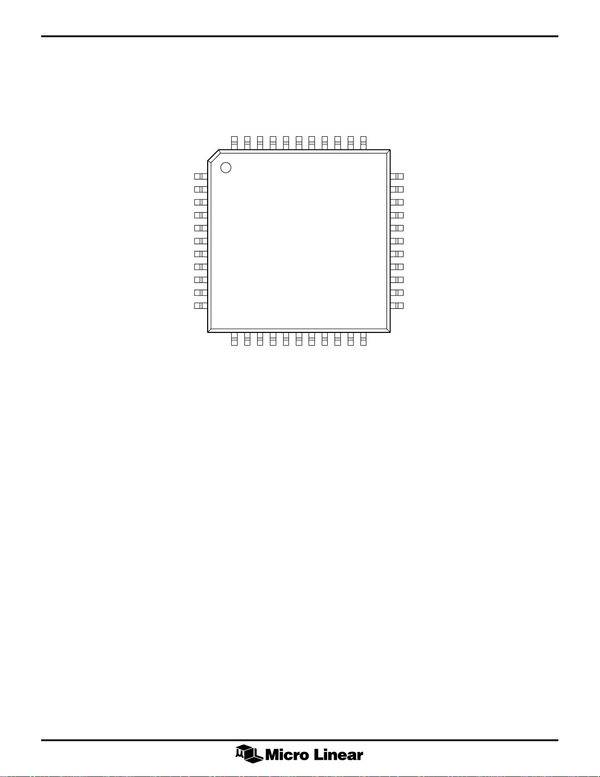
PIN CONFIGURATION
ML6440
44-Pin TQFP (H44-14)
C2
C1
C0
GND
V
CC
RST
CLK
CI0/DI0
CI1/DI1
CI2/DI2
CI3/DI3
C3C4C5C6C7
44 43 42 41 40
44 43 42 41 40
1
1
2
2
3
3
4
4
5
5
6
6
7
7
8
8
9
9
10
10
11
11
12 13 14 15 16
12 13 14 15 16 17 18 19 20 21 22
CI4/DI4
CI5/DI5
CI6/DI6
VCCGNDY0Y1Y2Y3
39 38 37 36 35 34
39 381937203621352234
17 18
CC
GND
AV
CI7/DI7
YI0/CV0
YI1/CV1
TOP VIEW
YI2/CV2
YI3/CV3
33
33
32
32
31
31
30
30
29
29
28
28
27
27
26
26
25
25
24
24
23
23
YI4/CV4
Y4
Y5
Y6
Y7
S CLK
S DATA
OE
S/P
YI7/CV7
YI6/CV6
YI5/CV5
2
Page 3

PIN DESCRIPTION
ML6440
PIN NAME FUNCTION
1 C2 Chrominance output
2 C1 Chrominance output
3 C0 Chrominance output
4 GND Digital ground pin
5V
6 RST Reset input active low. Resets comb
7 CLK TTL compatible clock reference
8 CI0/DI0 (LSB) Input Chrominance signal (PAL/
9 CI1/DI1 Input Chrominance signal (Square
10 CI2/DI2 Input Chrominance signal. (Comb
11 CI3/DI3 Input Chrominance signal (Comb
CC
Digital supply pin
logic including the internal data
register. Required at power up.
NTSC control pin in control pin mode:
register bit D0)
Pixel/CCIR control pin in control pin
mode: register bit D1)
mode 0 control pin in control pin
mode: register bit D2)
mode 1 control pin in control pin
mode: register bit D3)
PIN NAME FUNCTION
20 YI2/CV2 Luma or composite video input signal
21 YI3/CV3 Luma or composite video input signal
22 YI4/CV4 Luma or composite video input signal
23 YI5/CV5 Luma or composite video input signal
24 YI6/CV6 Luma or composite video input signal
25 YI7/CV7 Luma or composite video (MSB) input
signal
26 S/P Serial/Parallel program mode. If high,
allows 8-bit parallel control using the
eight digital chrominance input pins.
Data clocks in on the positive edge
transition. If low, serial port active.
27 OE Output enable. (Y[7:0] and C[7:0]) If
low, outputs high impedance.
28 S DATA Serial data input
29 S CLK Serial clock input. Positive-edge
clocks.
30 Y7 TTL compatible luminance output
(MSB)
31 Y6 Luminance output
12 CI4/DI4 Input Chrominance signal (Adaption
Threshold 0 control pin in control pin
mode: register bit D4)
13 CI5/DI5 Input Chrominance signal (Adaption
Threshold 1 control pin mode: register
bit D5)
14 CI6/DI6 Input Chrominance signal (Adaption
Threshold 2 control pin mode: register
bit D6)
15 CI7/DI7 (MSB) Input Chrominance
(Y+C/YI control pin in control pin
mode: register bit D7)
16 AV
17 GND Ground pin for analog delay line
18 YI0/CV0 TTL compatible (LSB) Input composite
19 YI1/CV1 Luma or composite video input signal
CC
Analog supply pin. Bypass to ground
with 1µF ceramic capacitor
video signal or Y in the Y+C bypass
mode
32 Y5 Luminance output
33 Y4 Luminance output
34 Y3 Luminance output
35 Y2 Luminance output
36 Y1 Luminance output
37 Y0 Luminance output (LSB)
38 GND Digital ground pin
39 V
40 C7 TTL compatible chrominance output
41 C6 Chrominance output
42 C5 Chrominance output
43 C4 Chrominance output
44 C3 Chrominance output
CC
Digital supply pin
(LSB)
3
Page 4
ML6440
ABSOLUTE MAXIMUM RATINGS
Absolute maximum ratings are those values beyond which
the device could be permanently damaged. Absolute
maximum ratings are stress ratings only and functional
device operation is not implied.
VCC............................................................................. 7V
Junction Temperature ............................................. 150°C
Storage Temperature Range...................... –65°C to 150°C
Lead Temperature (Soldering, 10 sec) ..................... 260°C
Thermal Resistance (
qJA) ...................................... 67°C/W
OPERATING CONDITIONS
Analog & Digital I/O ............. GND – 0.3V to VCC + 0.3V
Input Current .......................................................... 20µA
Temperature Range ........................................ 0°C to 70°C
VCC Range ...............................................4.75V to 5.25V
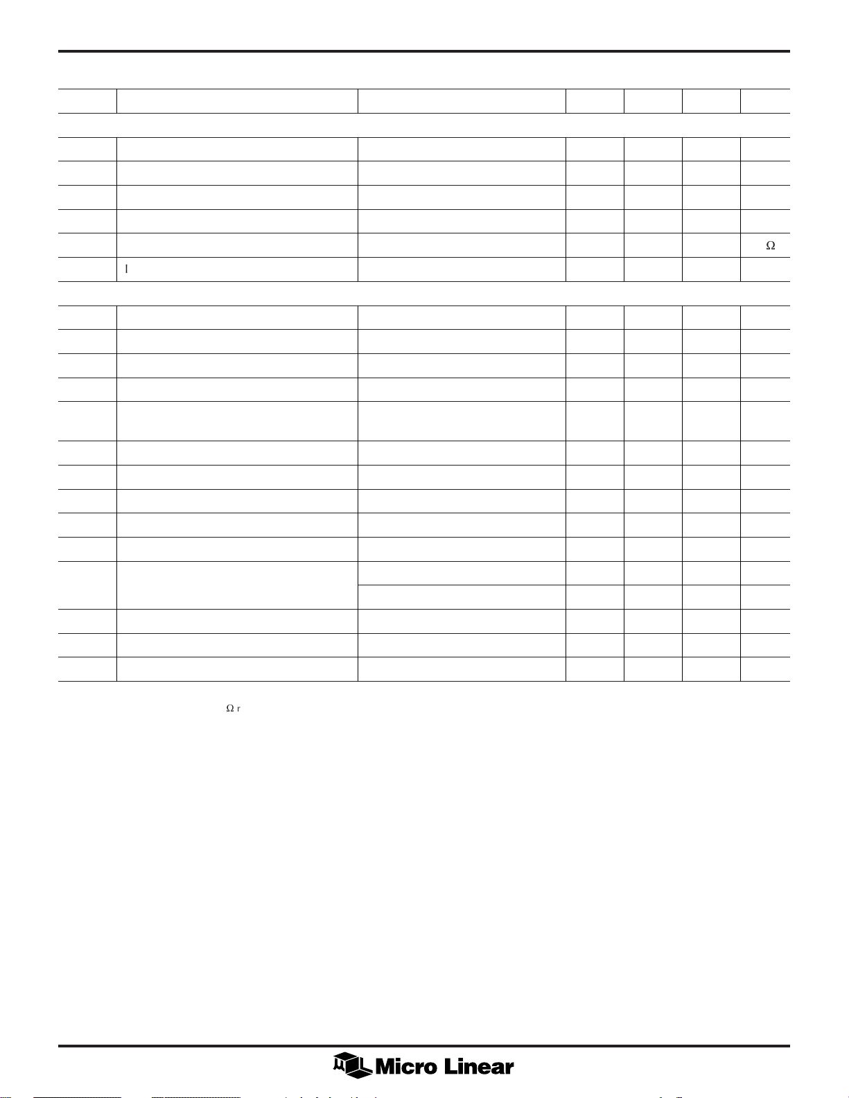
ELECTRICAL CHARACTERISTICS
Unless otherwise specified, VCC = 5V ±5%, CL = 50pF, TA = Operating Temperature Range (Notes 1, 2)
SYMBOL PARAMETER CONDITIONS MIN TYP MAX UNITS
SUPPLY
I
CC
AV
LOGIC
V
V
I
I
C
V
V
Supply Current VCC=5.25V, CLK=14.75 MHz, 60 90 mA
PAL Square Pixel
Analog Supply Voltage Recommend Operation VCC–0.6 VCC–0.4 V
CC
Low Level Input Voltage 0.8 V
IL
High Level Input Voltage V
IH
Low Level Input Current 10 µA
IL
High Level Input Current 10 µA
IH
Input Capacitance 5pF
IN
Low Level Output Voltage IOL = –2mA 0.4 V
OL
High Level Output Voltage IOH = 2mA VCC – 1.0 V
OH
Output Current 3-state Mode 10 µA
– 1.5 V
CC
C
OUT
SYSTEM TIMING
f
CLK
t
SU
Output Capacitance 3-state Mode 5 pF
CLK Input Frequency Square Pixel PAL 14.75 MHz
Setup Time to Rising CLK Edge f
Clock Low Duration f
Clock High Duration f
Input Rise Time f
Input Fall Time f
Data Valid after Rising CLK Edge f
3-state Delay Time, Output Enable f
3-state Delay Time, Output Disable f
Output Rise time f
Output Fall time f
4
Square Pixel NTSC 12.70 MHz
CCIR601 13.50 MHz
= 14.75MHz 10 ns
CLK
= 14.75MHz 30 ns
CLK
= 14.75MHz 45 ns
CLK
= 14.75MHz, 10% to 90% 20 ns
CLK
= 14.75MHz, 90% to 10% 20 ns
CLK
= 14.75MHz 20 ns
CLK
= 14.75MHz 20 ns
CLK
= 14.75MHz 20 ns
CLK
= 14.75MHz, 10% to 90% 20 ns
CLK
= 14.75MHz, 90% to 10% 20 ns
CLK
Page 5
ML6440
ELECTRICAL CHARACTERISTICS (Continued)
SYMBOL PARAMETER CONDITIONS MIN TYP MAX UNITS
VIDEO SIGNAL PROCESSING
Effective Luminance Bandwidth NTSC/PAL, Comb On at –3dB (Note 3)
NTSC/CCIR601, Comb Off at –3dB 2.5 MHz
NTSC/Sq. Pixel , Comb Off at –3dB 2.5 MHz
PAL/CCIR601 , Comb Off at –3dB 2.5 MHz
PAL /Sq. Pixel, Comb Off at –3dB 2.5 MHz
Effective Chrominance Bandwidth NTSC/PAL, Comb On at –3dB (Note 3)
Centered at f
COMB FILTER CHARACTERISTICS
SNR
SNR
Signal to Noise Ratio, Chrominance Spurious Luma Artifact NTSC 48 dB
C
Signal to Noise Ratio, Luminance Spurious Subcarrier NTSC 48 dB
L
Comb Notch Depth at f
Comb Notch Bandwidth at –30dB 500 kHz
SC
SC
NTSC/CCIR601, Comb Off at –3dB 1.0 MHz
NTSC/Sq. Pixel, Comb Off at –3dB 1.0 MHz
PAL/CCIR601, Comb Off at –3dB 1.0 MHz
PAL /Sq. Pixel, Comb Off at –3dB 1.0 MHz
13.5MHz
PAL 45 dB
12.27MHz
Artifact 13.5MHz
PAL 45 dB
12.27MHz
NTSC/PAL –35 dB
5
Page 6
ML6440
ELECTRICAL CHARACTERISTICS (Continued)
SYMBOL PARAMETER CONDITIONS MIN TYP MAX UNITS
SERIAL BUS LOGIC INPUT
Low Level Input Voltage 0 0.8 V
High Level Input Voltage VCC – 0.8 V
Low Level Input Current VIN = 0V 1.0 µA
High Level Input Current VIN = VCC D 1.0 µA
Input Impedance f
Input Capacitance (CIN)2pF
SYSTEM TIMING
S
CLK
Input Hysteresis (V
Spike Suppression (t
Power Setup Time to Valid Data Inputs VCC Settled to Within 1% 10 ms
Wait Time From STOP to START
On S
Hold Time for START On S
Setup Time for START On S
Min LOW Time On S
Min HIGH Time On S
Hold Time On S
Setup Time On (t
Frequency (f
(t
DATA
WAIT
CC
= 100kHz 1 M
CLK
) 100 kHz
CLOCK
) 0.2 V
HYS
) Max length for zero response 50 ns
SPIKE
) 1.3 µs
DATA (tHD/START
DATA (tSU/START
(t
CLK
LOW
(tHI) 0.6 µs
CLK
DATA (tHD/DATA
SU/DATA
) Fast mode (Note 4) 100 ns
) 1.3 µs
) 5.0 µs
) 0.6 µs
) 0.6 µs
Slow mode (Note 4) 250 ns
V
W
Rise Time for S
Fall Time for S
Setup Time for STOP On S
Note 1: Limits are guaranteed by 100% testing, sampling, or correlation with worst case test conditions.
Note 2: Supply voltage fed through 7.5W resistor to all VCC pins.
Note 3: No bandlimiting is performed on the signal bandwidth when the comb is in the “on” state.
Note 4: Parameter is luma dependent
CLK
CLK
& S
& S
DATA (tLH
DATA (tHL
DATA (tSU/STOP
) 30 300 ns
) 30 300 ns
) 0.6 µs
6
Page 7

FUNCTIONAL DESCRIPTION
ML6440
The ML6440 is an adaptive digital comb filter that offers
automatic self-adjusting or manual thresholds to handle
vertical and horizontal contouring during Y/C separation.
The ML6440 implements a SmartComb algorithm where
full bandwidth video and artifact suppression techniques
are used to automatically select suppression thresholds for
all video content. Video artifacts such as hanging dots, dot
crawl, and cross luminance are dramatically reduced. The
algorithm functionally performs a statistical analysis of the
video content of over 60 lines. It then calculates and
selects the best threshold for artifact reduction at 12-bit
resolution.
The ML6440 is a comb for NTSC (525 lines) and PAL (625
lines) with the ability to handle CCIR601 and square pixel
sampling rates.
CCIR601 is the existing standard for digitized video of
either NTSC or PAL at a 13.5MHz rate, and is used by
MPEG encoders and decoders for image compression. The
comb algorithms in the comb filter substantially reduce
rainbow and dot-crawl artifacts which interfere with
efficient image compression.
Square pixel is video digitized at 12.27MHz for NTSC,
and 14.75MHz for PAL, so that each sample corresponds
to a single pixel in computer displays without the effort or
expense of a multi-phase image resizing filter done in
hardware or software.
Using the ML6440 comb filter requires no external
components for operation. The comb filter can be
bypassed to accommodate selection of external S-video
signals. The comb filter is controllable via parallel pin or
serial interface.
SMARTCOMB OPERATION
The user supplies 8-bit video as either digital Y/C or digital
composite video inputs and receives delayed and combed
data at the Y/C digital outputs. Use of Y/C input assumes
that combing is unnecessary and sends the data through
the same delay as the composite video path to prevent
shifting of the video position on the screen. This makes the
ML6440 useful in source selection such as S-video inputs
and composite video. Composite video (CV), applied to
the ML6440 with comb operation enabled, permits the
separation of luminance and chrominance with minimal
artifacts.
The SmartComb controls the application of the comb filter
and bandsplit-notch filters on a pixel-by-pixel basis. The
digital video image is sampled, and an analysis is
performed. SmartComb step 1: looks for differences in the
low frequency spectra (vertical detail). SmartComb step 2:
searches for changes in phase angle/saturation of the
chroma sub-carrier, which represents changes in color in
the vertical direction. Finally, SmartComb step 3: an
averaging circuit is used as "smoothing function" to
eliminate dithering in the horizontal dimension caused by
excessive filter switching.
Figure 1 provides a simplified block diagram of the
SmartComb architecture. This architecture implements
several complex computations to determine the amount of
notch vs. comb filtering. Three 8-Bit detectors are used to
examine vertical and horizontal detail for luma and
chroma signals on a pixel-by-pixel basis for 3-line
analysis. These data are then fed into a weighting function
to determine the best filtering approach over the existing
3-lines of video. Furthermore, this data is then compared
CV
IN
HI-BAND
LOW BAND
LUMA VERTICAL
DETAIL DETECTOR
8-BIT
LUMA HORIZONTAL
DETAIL DETECTOR
8-BIT
CHROMA VERTICAL
DETAIL DETECTOR
8-BIT
1H
HI-BAND
LOW BAND
COMB/NOTCH
CONTROL FUNCTION
24-BIT, 3-LINE
COMB/NOTCH
THRESHOLD SELECT
MANUAL
THRESHOLD
SELECT
1H
COMP
COMB/NOTCH
CONTROL FUNCTION
12-BIT, FRAME, 60-LINE
Figure 1. SmartComb Architecture: Simplified Block Diagram
HI-BAND
LOW BAND
FADER
VIDEO
SIGNALS
MIXER
8-BIT
AUTOMATIC
THRESHOLD
SELECT
Y
OUT
C
OUT
7
Page 8

ML6440
PREAMBLE DATA ADDRESS (B3)
HEX
DATA (D[7:0]2)
Table 1. Serial Data Format
BIT D7 D6 D5 D4 D3 D2 D1 D0
Mode—Function Y+C or CV Adaption Adaption Adaption Comb Comb Square Pixel/ PAL
Select Threshold Threshold Threshold Mode Mode CCIR601 or NTSC
2 1 0 1 0 Select Select
Value Y+C = 1 AT2 = 0 AT1 = 0 AT0 = 0 CM1 = 0 CM0 = 0 Sq. Pixel = 1 PAL = 1
CV = 0 or 1 or 1 or 1 or 1 or 1 CCIR601 = 0 NTSC = 0
Parallel Mode CI7/DI7 CI6/DI6 CI5/DI5 CI4/DI4 CI3/DI3 CI2/DI2 CI1/DI1 CI0/DI0
Input Pin
Table 2. Control Register Format D[7:0] (Serial or Parallel Mode)
STANDARD/RATE CCIR601 SQUARE PIXEL
NTSC (f
PAL (f
= 3.58MHz) 13.5MHz 12.27MHz
SC
= 4.43MHz) 13.5MHz 14.75MHz
SC
Table 3. Clock Frequency Requirements
ADAPTION THRESHOLD D[6,5,4] ADAPTION THRESHOLD LEVEL
000 Automatic threshold for minimal comb artifact generation for various video
source material.
001 Threshold for computer graphics applications, minimizing dot crawl on
bold lettering.
010 to 110 Various degrees of thresholds.
111 Threshold for better reproduction of natural photographic images.
Table 4. Adaption Threshold Bit Table
COMB MODE, D[3,2] NTSC PAL
00 Y adaptive, C comb 100% active Y adaptive, C adaptive
01 Y adaptive, C adaptive Y adaptive, C comb 100% active
10 Y 100% comb active, C 100% comb active Y 100% comb active, C 100% comb active
Not recommended due reduced performance
11 Bandsplitting only (no combing) Bandsplitting only (no combing)
Table 5. Comb Mode Bit Table
8
Page 9

S DATA
ML6440
START
t
RISE
t
SET/START
S CLK
START: A Falling Edge on the S DATA While S CLK is Held High
STOP: A Rising Edge on the S DATA While S CLK is Held High
All Other S DATA Transitions Must Occur While S CLK is Low
Figure 2. Definition of START & STOP on Serial Data Bus
S DATA
S CLK
MSB MSB
A1 A0A6A7
0 1 2 7 8 9 10 11 16 17 18
9th pulse strobes address decoder
S CLK:
Rising edge enables data transfer
S CLK:
Value set to A6, Device Address (MSB-1)
S DATA:
Falling edge disables data transfer
S CLK:
Rising edge enables data transfer
S CLK:
Value set to A7, Device Address MSB
S DATA:
Falling edge in prep for first address transfer
S CLK:
Falling edge w/S CLK high means start of sequence
S DATA:
D7 D6 D1 D0
S DATA:
S DATA:
S CLK:
S CLK:
S DATA:
S CLK:
S CLK:
S DATA:
t
FALL
STOP
STOP
Rising edge with S CLK Hi = STOP
Value set low in prep for STOP
18th pulse strobes data shift register
Rising edge enables data transfer
Value set to D6, Data MSB-1
Falling edge disables data transfer
Rising edge enables data transfer
Value set to D7, Data MSB
Figure 3. Definition of DATA FORMAT on Serial Data Bus
S DATA
‘1’ ‘0’ ‘0’ ‘1’ Ø ØD7 D6 D5 D4 D3 D2 D1 D0‘0’‘1’ ‘1’ ‘1’
S CLK
0 1 2345 9ABCD E FGH I
DEVICE ADDR = ‘B3’ CONTROL REGISTER
687
S CLK:
Address decode strobed on 9th clock
[Data is ‘don’t care’ during strobe]
‘1011 0011’ shifted on next 8 clocks
S DATA:
Falling edge in prep for device address transfer
S CLK:
S
:
Final Clock strobes data into register
DATA
Control register, load MSB first
Figure 4. Typical Serial Bus Command
STROBE (ACK)
9
Page 10

ML6440
FUNCTIONAL DESCRIPTION (Continued)
to the video content of the last 60+ lines (frames) of video
—a frame weighing function— to determine the best
filtering approach of the current video content. Finally, 1
of 7 thresholds can be chosen to adjust either real-time
(automatically) by the ML6440 itself or fixed manually by
design. An internal 12-bit analysis is used for the filtering
algorithm. An additional fader circuit is included to
"smooth" the transitions between comb and notch filtering.
In NTSC, every other line of chroma is inverted while
there are no changes in luma (assuming there is no change
in color between adjacent lines). This permits data to be
added from the first stored line of data with the third line
of active high-band video data, each with a scaling of
0.25, and add the second stored line of data with a scaling
of 0.50. The result contains no chroma, only luma
information. Subtracting this information from the highband signal yields only chroma information.
In PAL, each line of data rotates the phase of the chroma
by 90 degrees. Therefore, by adding the first line of stored
high-band information from the active third line, the
chroma is canceled, leaving only luma information. Once
again, this information is subtracted with the appropriate
amplitude scaling from the original highband information
to yield only chroma.
The bandsplit-notch and comb filters were designed to
reduce color bar peak-to-peak dot edge crawl to <7.5%
for 75% color bars. Peak-to-peak cross color on the white
bar edge was designed to be <1% with 75% color bars.
SERIAL PROGRAM MODE
In Serial Program Mode, the comb filter can be controlled
with the serial interface. Control inputs may be clocked in
serially with S DATA and S CLK , when S/P is low. Serial
bus transfers require an 8-bit address followed by 8-bits of
data for the internal data register. The pattern is described
in Tables 1 through 5.
The serial bus control in the ML6440 has one level of
addressing followed by control register programming.
Figure 2 shows the physical waveforms generated in order
to address the ML6440. There are six basic parts of the
waveform:
1. Start indication: Clock Cycle 0
2. Device address shifted in: Clock Cycle 1 thru 8
3. Device address strobed /decoded: Clock Cycle 9
4. Data shifted in: Clock Cycle 10 thru 17
5. Data strobed to appropriate register: Clock Cycle 18
6. Stop indication: Clock Cycle 19
In bandsplit (notch) filtering and luma peaking, the digital
bandsplit filter is used as an alternate filter when the
SmartComb algorithm determines that the comb filter
output signal would be contaminated with cross chroma
artifacts. To maintain a reasonable amount of apparent
resolution in the luminance signal, luma peaking is
applied. This helps maintain image quality in the portion
of the video image where comb filtering would generate
artifacts.
The ML6440 SmartComb provides a real-time filtering
algorithm solution (automatic mode) for a wide variety of
video sources without the shortcomings of using fixed
thresholds (manual mode). The automatic threshold
tracking circuit responds quickly, adjusting itself in about
1/300th of a second (about 60 lines). The transition from
the comb to the digital bandsplit is made with a
continuous digital fader to prevents switching glitches.
RST
POWER ON
PARALLEL PROGRAM MODE
In Parallel Program Mode, the CI/DI[7:0] pins act as
programming pins for the internal 8-bit register (D[7:0])
such that CI7/DI7=D7, CI6/DI6=D6, ... CI0/DI0=D0. In
the parallel mode, the S/P serves as a rising edge-triggered
strobe pin for the internal registers of D[7:0]. When S/P
goes from low to high, data applied to the inputs (CI/
DI[7:0]), is loaded into the internal 8-bit register D[7:0]
directly. A transition on the S/P pin back to low will
reactivate the serial mode. If the S/P is held at a high, the
serial mode is inactive.
CONTROL REGISTER, D[7:0]
The internal register, D[7:0], controls the following
functions within the ML6440. Again, this register can be
programmed through either a serial or parallel interface.
The RST acts as a reset pin, forcing all the bits of the
AT LEAST 1µs LOW
10
AT LEAST 5µs HIGH
Figure 5: Reset Timing
Page 11

FUNCTIONAL DESCRIPTION (Continued)
ML6440
internal data register low (D[7:0]=0) which defaults to
automatic combing of NTSC/CCIR601 composite video.
The Y+C/CV selection bit, D7, controls whether Y+C or CV
format is the source for the comb filter. Setting this bit low
selects the composite input pins, which is combed by
default. Setting the bit high selects the Y+C inputs as the
source for video (see bypass section). This source is not
combed and the Y+C inputs are not activated until the S/P
pin is rising-edge triggered.
Adaption thresholds 2 through 0 are D6 through D4,
respectively. These set the adaption behavior from
automatic (D[6:4]=000) to one of seven settings ranging
from fine tuning of computer graphics to photographic
images. See Table 4.
Comb modes 1 and 0, (D3 and D2, respectively) are used
to enable and disable adaption separately on Y and C
data. For NTSC, if D[3:2]=<00>, then Y is adaptive and C
is always combed. For NTSC, if D[3:2]=<01>, both Y and
C are adaptive. For PAL, if D[3:2]=<00>, then both Y and
C are adaptive. For PAL, if D[3:2]=<01>, then Y is
adaptive and C is combed. For NTSC and PAL, if
D[3:2]=<10>, then Y and C are forced to comb mode. For
NTSC and PAL, if D[3:2]=<11>, then both Y and C are in
bandsplit filtering mode only. See Table 5.
The RST pin resets the comb logic including the internal
data register on active low but does not clear the line
delays. This part requires a timed reset pulse. On power
up or at any time a return to automatic combing of NTSC/
CCIR601 composite video is required the reset pin must
have been high for at least 5 micro seconds. Then taken
low for at least one micro second before returning high
again to resume normal operation. Neither pulse width
nor rise and fall times are critical.
In most applications a microprocessor will be available to
provide timing and control waveforms. It will provide this
reset pulse and if needed set the appropriate comb filter
mode. In non processor systems an R C network can
provide this reset pulse. See Figure 5.
CHROMA AND LUMA BYPASS OPERATION
This mode can be activated by setting the internal bit
D7 = 1 either through the serial or parallel programming
modes. Once the register is set (D7 = 1), the comb filter
will look at the inputs for luma on the CV[7:0] pins for a
luma bypass to the outputs of the Y[7:0] pins respectively;
as well as inputs for chroma on the CI/DI[7:0] pins for a
chroma bypass to the outputs of the C[7:0] pins
respectively. The comb filter will continue to look at the
inputs as long as D7 is set high.
The D1 bit sets the choice of data rates between CCIR601
and Square pixel. CCIR601 is active low. Square pixel is
active high. The last bit, D0, select the standard, NTSC or
PAL. NTSC is active low. PAL is active high. See Table 2.
The remaining pin function controls are independent of
the data register: CLK, RST, and OE. The CLK pin requires
a clock at the rates listed in Table 2. Its duty cycle must
meet the duration minimum for high and low.
60%
13.5MHz CLOCK
20ns
Y/C OUTPUT
Data presented to the inputs (CI/DI[7:0]) is not interrupted
in the color processing path when S/P is held high or low.
Therefore, it is recommended that S/P activity be limited to
sync or blanking intervals in the video to avoid unwanted
visual artifacts during register programming.
Clock Timing
Figure 6 depicts digital video input and output timing for
valid data.
40%
Y OR C DATA
15ns 0ns
Y OR C DATA
CV INPUT
CV DATA
Figure 6: Clock Timing
CV DATA
11
Page 12

ML6440
TYPICAL APPLICATIONS
Figure 7 depicts an application block diagram of the
ML6440. The ML6440 is easy to use in most standard
video applications in conjunction with an 8-bit A/D
converter or digital data for analog and digital
applications. High speed digital layout should be
observed. Pay special attention that the outputs are not
loaded beyond a 2mA load. An A/D, if used, should have
at least seven effective bits at Nyquist rates for good
quality video. Please note that startup of the part will
require at least two lines to flush out the line delays and
about 10 lines for the adaption to adjust. The automatic
adaption thresholding should not be discernible in most
video applications, but can be defeated with the fixed
adaption levels. In applications using video tape recorders
the comb may not be effective and can make results worse
if time jitter exceeds the clock period 70ns. Jitter of this
magnitude would misalign the line delays, making the
combing and adaption incorrect. In this case combing
should be turned off.
POWER SUPPLY REQUIREMENTS
The AV
0.4V drop from a 5V supply. Alternately, a 7.5W resistor
can be used instead of the diode. The AV
a 1µF surface mount capacitor to ground. See Figure 7.
Bypass caps must be within 3mm of the chip pins they
bypass. Direct traces are necessary.
Digital Video Values of Sync Tip and Peak White
As recommended by SMPTE and ITU-R BT.601, the
minimum value of digitized sync tip is decimal 16. The
maximum value of digitized video is decimal 255 (235
recommended is by SMPTE which allows for overshoots in
video). Normally, peak white is at 235; this avoids
clipping due to overshoots.
Figure 8 presents Micro Linear’s entire solution for
optimized video application designs. The ML6430 can be
used as high performance line lock clock that’s capable of
must be fed through a Schottky diode of about
CC
pin also needs
CC
generating horizontal and vertical syncs and a variety of
system clocks using common reference frequency crystals.
The ML6401 is a low cost A/D converter. The ML6421 is a
three channel filter with sinx/x equalization. The ML6424
is a precision filter used as a clamp circuit and antialiasing filter. (See Micro Linear's ML6440EVAL for more
information)
Test Patterns
When viewing test patterns, the fixed thresholds may give
better performance, since the automatic adaptive
threshold algorithm was optimized for live video.
There are various specific application uses of the ML6440
SmartComb :
• Large screen TVs
• HDTV
• Video projection
• MPEG encoding
• Video conferencing
• Imaging and video capture
• Format converters
• Time base correctors
• Professional video
• Line doublers and quadrapulers
Figure 9 illustrates the use of the ML6440 in a big screen
TV application. In this application, the ML6440 offers
automatic self-adjusting thresholds to optimize Y/C
separation while minimizing artifacts for a wide variety of
live video material without fixed threshold limitations. The
ML6440 supports S-video bypass or luma and chroma
separation enhancement, simplifying design for highperformance video source selection.
Figure 10 illustrates the use of the ML6440 in HDTV and
NTSC application. In hybrid TV sets, where both NTSC
and HDTV will be prevalent, the ML6440 SmartComb can
serve as a high-performance Y/C NTSC-separator in a
NTSC-HDTV video receiver.
12
Page 13

TYPICAL APPLICATIONS (Continued)
ML6440
5V
RESET
GENLOCK,
SYSTEM CLOCK
CV IN
SERIAL/PARALLEL (S/P)
OUTPUT ENABLE (OE)
SERIAL DATA IN (S DATA)
SERIAL CLOCK (S CLOCK)
CLAMP
FILTER
A/D
1µF
PARALLEL OR CHROMA
8
1
2
3
4
5
6
7
8
9
10
11
BYPASS INPUT
1µF
44 43 42 41 40
12 13 14 15 16 17 18 19 20 21 22
39 38 37 36 35 34
ML6440
SmartComb
*
1µF
5V
8
D/A CHROMA
8
D/A
33
32
31
30
29
28
27
26
25
24
23
FILTER
FILTER
LUMA
PIN 16
*
7.5Ω
5V
ALTERNATIVE
POWER SUPPLY
1µF
Figure 7. Typical Application Circuit
13
Page 14

ML6440
TYPICAL APPLICATIONS (Continued)
S VIDEO
COMPOSITE
VIDEO
ML6424
TUNER
FILTER
ML6431
GENLOCK
IF
ML6401
A/D
ML6440
COMB
FILTER
8
CLOCK
8
8
8
D/A
D/A
D/A
Figure 8. Micro Linear Application Solution
HDTV
PLL
HDTV
DETECTOR
NTSC
DETECTOR
DIGITAL
MPEG
DECODER
YUV
ML6421
FILTER
FILTER
FILTER
Y
C
CV
MUX MATRIX
LUMA
CHROMA
COMPOSITE
VIDEO
TO
DISPLAY
COMPOSITE VIDEO IN
COMPOSITE VIDEO
FROM TV TUNER
S VIDEO LUMA
S VIDEO CHROMA
GENLOCK
ML6440
SmartComb
CHROMINANCE
DEMODULATOR
YUV
Figure 9. Application Diagram: HDTV and NTSC Television
GENLOCK
CVIN/Y
MUX
A/D
A/D
IN
C
IN
ML6440
SmartComb
SERIAL
BUS
CONTROL
LUMA
CHROMA
CHROMINANCE
DEMODULATOR
Figure 10. Application Diagram: High-end Television/Monitor
R
MATRIX
U
V
G
B
TO
CRT
14
Page 15

PERFORMANCE DATA
ML6440
COMB FILTER PERFORMANCE
• Unrestricted Bandwidth. No band-limiting is performed
on the signal when the comb is on hence preventing a
signal loss.
• High frequency peaking allows for gentle transitions
from comb to notch modes.
• Spurious sub-carrier supression by 48dB removes color
sub-carrier which otherwise can cause large area dot
crawl
NOTCH FILTER PERFORMANCE
• When invoked by adaption threshold logic, hanging dot
suppression is 35dB.
ADAPTIVE THRESHOLD PERFORMANCE
• Seven fixed values to select threshold, the 8th value is
for automatic self-adjusting threshold mode.
• Adaptive thresholds improve around 10% per threshold
level. However, adaptive thresholds can surpass
optimum threshold thus causing smearing effects.
• D[6:4] = 000 is the automatic self-adjusting threshold
mode. D[6:4] = 001 is the low threshold and D[6:4] =
111 is the highest threshold, D[6:4] = 010 to 110 is
therefore the intermediate thresholds.
Figures 11 through 20 show the bandwidth of notch,
chroma bandpass, and comb filters for NTSC and PAL
video. These curves were taken from a VM700 using a
sweep frequency pattern using a TG2000 on the
ML6440EVAL board.
Figure 11 shows the NTSC luma filter at CCIR clock rates.
This shows significant notch from 3.3MHz to 4MHz
sufficient for hanging dot suppression. Figure 12 shows
the NTSC chroma bandpass filter for CCIR clock rates
where the filter at 3dB ranges from 3MHz to 4.5Mhz.
Figure 13 shows the luma notch filter for NTSC for
hanging dot suppression for Square Pixel clock rates. This
notch ranges from 3.3MHz to 4MHz. Figure 14 shows the
NTSC chroma bandpass filter running at Square Pixel
clock rates where it at 3dB ranges from 3MHz to 4.5MHz.
Figure 15 shows PAL luma response for hanging dot
suppression at Square Pixel clock rates where notch
ranges from 3.3MHz to 4MHz. Figure 16 shows the
response of the PAL chroma bandpass filter where at 3dB
down ranges from 3MHz to 4.2MHz. Figure 17 shows the
PAL notch filter for luma hanging dot suppression at CCIR
clock rates where the notch ranges from 4MHz to 4.3MHz
at zero amplitude. Figure 18 shows the bandpass filter for
PAL at the CCIR clock rate where at 3dB down ranges
from 3.3MHz to 4.7MHz. Figure 19 shows the NTSC
luma comb response over a line-to-line in phase
frequency sweep to 6MHz for CCIR clock rates. Figure 20
shows the NTSC luma response over a line-to-line in
phase frequency sweep to 6MHz for Square Pixel clock
rate.
1.5
1.0
0.5
AMPLITUDE (V)
0
–0.5
1
02 64
35
FREQUENCY (MHz)
Figure 11. NTSC Luma Notch Filter CCIR
1.5
1.0
0.5
AMPLITUDE (V)
0
–0.5
1
02 64
35
FREQUENCY (MHz)
Figure 12. NTSC Chroma Band Phase Filter, CCIR
15
Page 16

ML6440
1.5
1.0
0.5
AMPLITUDE (V)
0
–0.5
1
02 64
35
FREQUENCY (MHz)
1.5
1.0
0.5
AMPLITUDE (V)
0
–0.5
1
02 64
35
FREQUENCY (MHz)
Figure 13. NTSC Luma Notch Filter, Square Pixel Figure 14. NTSC Chroma Band Pass at Square Pixel
Clock
1.5
1.0
1.5
1.0
0.5
AMPLITUDE (V)
0
–0.5
1
02 64
35
FREQUENCY (MHz)
0.5
AMPLITUDE (V)
0
–0.5
1
02 64
35
FREQUENCY (MHz)
Figure 15. PAL Luma Notch Filter, Square Pixel Clock Figure 16. PAL Chroma Band Pass Filter, Square Pixel
Clock
1.5
1.0
0.5
AMPLITUDE (V)
0
1.5
1.0
0.5
AMPLITUDE (V)
0
16
–0.5
1
02 64
35
FREQUENCY (MHz)
Figure 17. PAL Luma Notch Filter
–0.5
1
02 64
35
FREQUENCY (MHz)
Figure 18. PAL Chroma Pand Pass, CCIR Clock Rate
Page 17

ML6440
1.5
1.0
0.5
AMPLITUDE (V)
0
–0.5
1
02 64
35
FREQUENCY (MHz)
1.5
1.0
0.5
AMPLITUDE (V)
0
–0.5
1
02 64
35
FREQUENCY (MHz)
Figure 19. NTSC Comb Luma, CCIR Clock Rate Figure 20. NTSC Luma Comb, Square Pixel
17
Page 18

ML6440
PHYSICAL DIMENSIONS inches (millimeters)
Package: H44-14
44-Pin (14 x 14 x 1mm) TQFP
0.630 BSC
(16.00 BSC)
0.551 BSC
(14.00 BSC)
34
0º - 7º
0.003 - 0.008
(0.09 - 0.20)
1
12
0.039 BSC
(1.00 BSC)
PIN 1 ID
0.014 - 0.020
(0.36 - 0.51)
ORDERING INFORMATION
PART NUMBER TEMPERATURE RANGE PACKAGE
ML6440CH (EOL) 0°C to 70°C 44 Pin TQFP (H44-14)
23
0.551 BSC
(14.00 BSC)
0.630 BSC
(16.00 BSC)
0.048 MAX
(1.20 MAX)
0.037 - 0.041
(0.95 - 1.05)
0.018 - 0.030
(0.45 - 0.75)
SEATING PLANE
© Micro Linear 2000. is a registered trademark of Micro Linear Corporation. All other trademarks are the
property of their respective owners.
Products described herein may be covered by one or more of the following U.S. patents: 4,897,611; 4,964,026; 5,027,116;
5,281,862; 5,283,483; 5,418,502; 5,508,570; 5,510,727; 5,523,940; 5,546,017; 5,559,470; 5,565,761; 5,592,128;
5,594,376; 5,652,479; 5,661,427; 5,663,874; 5,672,959; 5,689,167; 5,714,897; 5,717,798; 5,742,151; 5,747,977;
5,754,012; 5,757,174; 5,767,653; 5,777,514; 5,793,168; 5,798,635; 5,804,950; 5,808,455; 5,811,999; 5,818,207;
5,818,669; 5,825,165; 5,825,223; 5,838,723; 5.844,378; 5,844,941. Japan: 2,598,946; 2,619,299; 2,704,176; 2,821,714.
Other patents are pending.
Micro Linear makes no representations or warranties with respect to the accuracy, utility, or completeness of the contents of
this publication and reserves the right to make changes to specifications and product descriptions at any time without notice.
No license, express or implied, by estoppel or otherwise, to any patents or other intellectual property rights is granted by this
document. The circuits contained in this document are offered as possible applications only. Particular uses or applications
may invalidate some of the specifications and/or product descriptions contained herein. The customer is urged to perform its
own engineering review before deciding on a particular application. Micro Linear assumes no liability whatsoever, and
disclaims any express or implied warranty, relating to sale and/or use of Micro Linear products including liability or warranties
relating to merchantability, fitness for a particular purpose, or infringement of any intellectual property right. Micro Linear
products are not designed for use in medical, life saving, or life sustaining applications.
2092 Concourse Drive
San Jose, CA 95131
Tel: (408) 433-5200
Fax: (408) 432-0295
www.microlinear.com
18
DS6440-01
 Loading...