

Page 1
December 1998
PRELIMINARY
ML6430/ML6431*
Genlocking Sync Generator with
Digital Audio Clock for NTSC, PAL & VGA
GENERAL DESCRIPTION
The ML6430/ML6431 are multi-standard single-chip
BiCMOS video Genlock ICs for NTSC, PAL and VGA.
They are designed to provide a stable clock from an
analog video signal, and to provide timing pulses for
clamping, decoding, blanking and processing video
signals. The ML6430/ML6431 handle VCR glitches and
variations created by head switching, tape dropouts,
missing sync pulses, freeze frames, high speed playback
and camcorder gyro errors. The ML6430/ML6431 are
designed for high noise immunity, insensitivity to varying
signal amplitudes, overmodulated color carriers, and sync
glitches. Advanced analog and digital clock synthesis
techniques provide multi-standard and non-standard
operation from a single crystal or external asynchronous
clock source. Pin selectable preset modes allow operation
for most video standards in simple stand-alone mode
without the necessity of using the serial bus. For more
demanding applications, a two wire serial control bus is
available for full control of all of the ML6430/ML6431
features.
The ML6430/ML6431 are ideal for clock generation in
MPEG encoders, high performance display timing, and
video editing.
FEATURES
■ Line locked scalable horizontal pixel clock for an
arbitrary number of pixels per line
■ Standard frequencies of 12.27, 13.5, 14.75MHz, or 4Fsc
■ 4´/2´ or 2´/1´ clock outputs (54 and 27MHz, or 27 and
13.5MHz) and VGA clocks
■ Audio clocks: 32, 44.1, or 48kHz, locked to video
■ On-chip sync separator, VCO and pulse generator
■ Low clock jitter: Short Term: <200ps rms locked
■ Line to line: <600ps rms (2.2ns peak-to-peak) locked
■ Fast recovery from VCR head switch, stable for fast
shuttle speeds and pause
■ Single crystal or external frequency source
■ PAL, NTSC or VGA operation
■ 2 wire serial control bus, or selectable presets for stand
alone operation
■ RS170A compatible
* This Part Is End Of Life As Of August 1, 2000
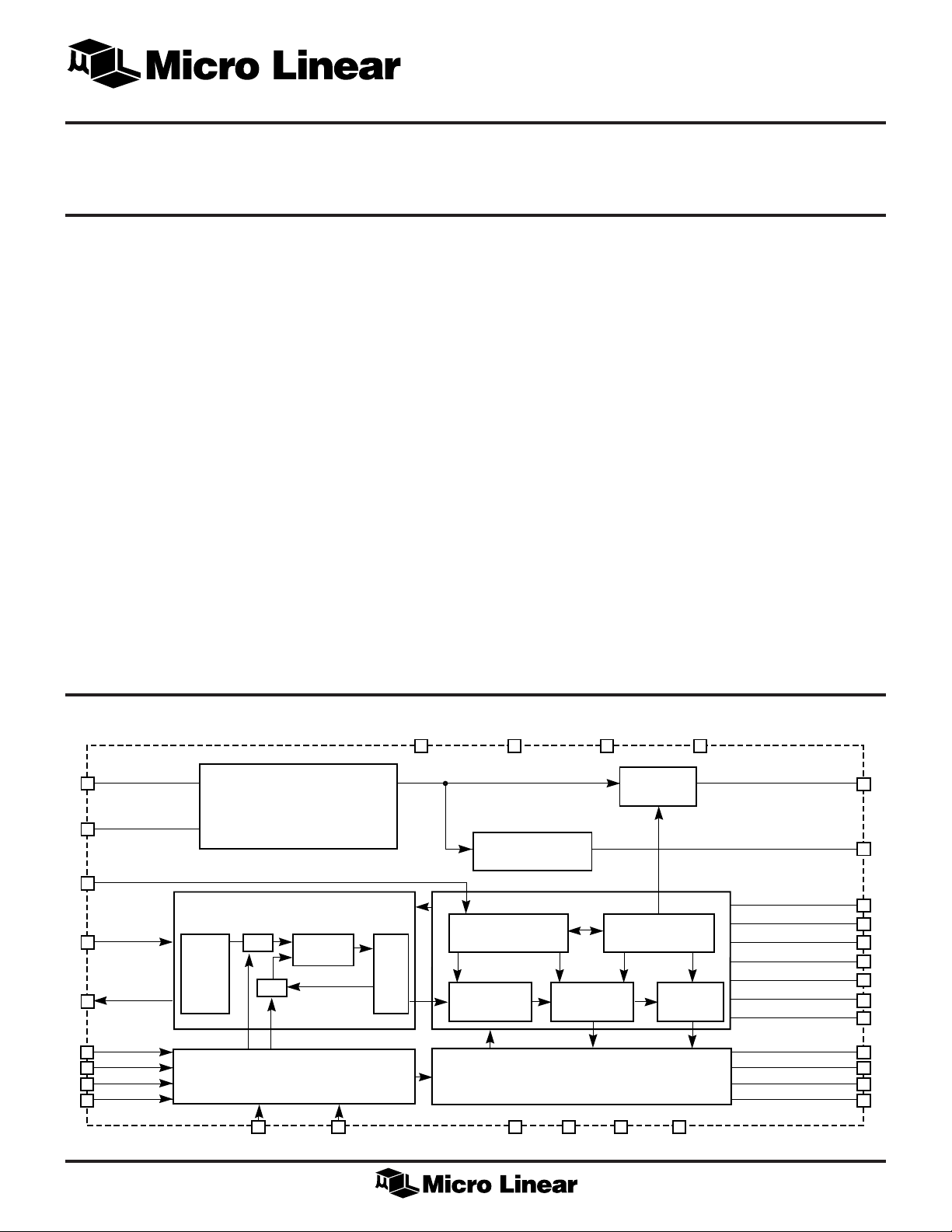
BLOCK DIAGRAM
C
VIN/
H
SYNC
6
CV
REF
7
V
SYNC
8
XTAL
IN
11
CRYSTAL
XTAL
12
P0
31
P1
32
P2/S DATA
1
P3/S CLK
2
OUT
OSC.
SLEEP/54MHz
V
SV
CC
SYNC SEPARATOR
ANALOG PLL
DIGITAL PHASE DET.
÷M
SERIAL CONTROL
AND PRESETS
3 13 5 10 20 30
÷N
PHASE
DETECTOR
FREERUN
REF
VCO
AND FILTERING
DIGITAL PHASE
AV
CC
SIGNAL DETECT
DIGITAL PLL
MOD.
GND S GND A GND B GND D
HORIZ. PIXEL
PULSE AND AUDIO
CLOCK GENERATOR
BV
CC
MUX
DYNA. STATE MACH.
CONTROLLER
COUNTER
292194
CC
VERT. LINE
COUNTER
D
B
1X CLOCK/4X CLOCK
AUDIOCLK/PHERROUT*
ONLY AVAILABLE IN ML6431
C
SYNC
NOSIGNAL
LOCKED
H
RESET
F
RESET
S
CLAMP
/BURST
CLAMP
2X CLOCK
H
BLANK
V
BLANK
FIELD ID
*PHERROUT IS
26
14
15
23
22
28
27
19
18
25
24
17
16
1
Page 2
ML6430/ML6431
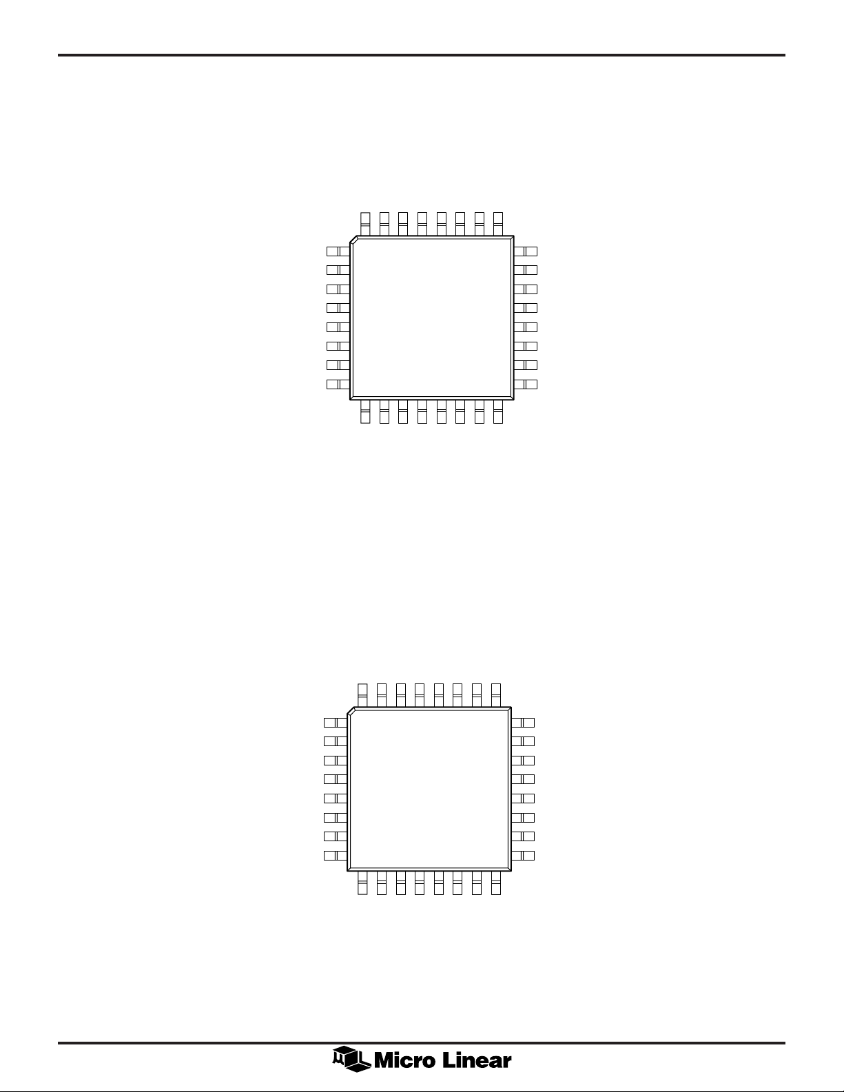
PIN CONFIGURATION
ML6430
32-Pin TQFP (H32-7)
D
P1P0GND D
CC
V
SCLAMP
BCLAMP/BURST
SYNC
C
HBLANK
P2/S
DATA
P3/S
CLK
SLEEP/54MHz
VCC S
GND S
C
VIN/HSYNC
CV
REF
V
SYNC
32 31 30 29 28 27 26 25
1
2
3
4
5
6
7
8
9 10111213141516
A
CC
V
GND A
XTALIN
XTALOUT
FREERUN
NOSIGNAL
LOCKED
TOP VIEW
ML6431
32-Pin TQFP (H32-7)
24
23
22
21
20
19
18
17
AUDIOCLK
VBLANK
HRESET
FRESET
V
B
CC
GND B
1X CLOCK/4X CLOCK
2X CLOCK
FIELD ID
P2/S
DATA
P3/S
CLK
SLEEP/54MHz
VCC S
GND S
C
VIN/HSYNC
CV
REF
V
SYNC
D
GND A
XTALIN
CC
V
SCLAMP
FREERUN
XTALOUT
BCLAMP/BURST
C
LOCKED
NOSIGNAL
P1P0GND D
32 31 30 29 28 27 26 25
1
2
3
4
5
6
7
8
9 10111213141516
A
CC
V
TOP VIEW
SYNC
HBLANK
24
23
22
21
20
19
18
17
VBLANK
HRESET
FRESET
V
CC
GND B
1X CLOCK/4X CLOCK
2X CLOCK
FIELD ID
AUDIOCLK/PHERROUT
B
2
Page 3

ML6430/ML6431
PIN DESCRIPTION (NOTE: ML6430 and ML6431 pin functions are identical
PIN NAME FUNCTION
1 P2/S
DATA
This is a dual function pin. If presets
are enabled, refer to Table 7. If presets
are disabled, serial bus data input.
2 P3/S
CLK
This is a dual function pin. If presets
are enabled, refer to Table 7. If presets
are disabled, serial bus clock input.
3 SLEEP/54MHz
Hardware sleep mode: when low,
disables entire chip for ultra-low
power dissipation. Sleep mode can
also be enabled/disabled via serial bus
(Register 8). 54MHz is a clock input.
This can be any 4X clock up to
70MHz used for pulse generation.
4V
S Analog supply for sync separator.
CC
5 GND S Analog ground for sync separator.
6CVIN/H
Composite video input; video input in
SYNC
typical composite video applications,
or Y input for YUV applications, or G
input for RGB applications with sync
on green. For typical VGA or other
high performance display applications, this input may be supplied with
a TTL level H
signal and the
SYNC
vertical sync input supplied with a TTL
level V
SYNC
signal.
PIN NAME FUNCTION
13 FREERUN Forces the PLL to run at a selected
standard without syncing to a video
signal. Accuracy is ±20ppm in
FREERUN with ideal crystal, otherwise
locked to video source
14 NOSIGNAL Indicates video signal activity has not
been detected at the composite input.
If NOSIGNAL = low, this condition
does not imply that lock has been
established. The NOSIGNAL pin can
be tied to FREERUN to create a local
loop in which the genlock will not try
to lock until a signal is detected at the
input.
15 LOCKED Indicates when digital PLL is locked to
incoming video signal.
16 (ML6430) AUDIOCLK
Digital audio clock output.
Programmable for 32kHz, 44.1kHz or
48kHz output.
16 (ML6431) AUDIOCLK/PHERROUT
This is a dual mode pin. Pin is selected
via serial bus (Register 7). AUDIOCLK
is an audio clock signal (see Table 9).
PHERROUT indicates whether
incoming HSYNC is ahead or behind
output HSYNC.
except
for pin 16. See below)
7CV
REF
Reference voltage for internal sync
slicer. The external capacitor is driven
by a charge pump to follow the sync
tip.
8V
SYNC
Vertical input for non-composite
sources. This input may be supplied
with a TTL level V
SYNC
signal. For
composite inputs this pin is tied high
or low.
9VCC A Analog supply pin for analog PLL.
10 GND A Analog ground for analog PLL.
11 XTAL
IN
Crystal may be parallel tuned 3.58
MHz or 4.43MHz, or may be driven
by an external oscillator at these
frequencies, or at 4x these
frequencies.
12 XTAL
OUT
Crystal drive pin. No connect if using
external oscillator or clock.
17 FIELD ID Field Flag: Odd = 1, Even = 0
18 2X CLOCK 2X oversampled PIXEL CLOCK &
Output of Digital PLL. Nominal
frequency of 27MHz
19 1X CLOCK/4X CLOCK
1X pixel clock. Nominal frequency
of 13.5MHz or 54MHz ±20ppm in
FREERUN with ideal crystal, otherwise
locked to video source. PAL 4X CLOCK
not available (no 4x4.4336MHz clock).
20 GND B Digital ground for output driver
buffers.
21 VCC B Digital supply for output driver buffers.
22 F
RESET
Frame reset; active low for one half
line at the high to low transition of
field ID. In NTSC mode, FRESET goes
low on the high-to-low transition on
the Field ID pin and at the beginning
of line 1 (see Figure 2). In PAL mode,
FRESET goes low on the high-to-low
transition on the Field ID pin and at
the end of line 310 (see Figure 3).
3
Page 4

ML6430/ML6431
PIN DESCRIPTION (Continued)
PIN NAME FUNCTION
23 H
24 V
25 H
26 C
27 B
RESET
BLANK
BLANK
SYNC
CLAMP
Horizontal reset; active low for one
half pixel.
Vertical blanking, active low
Horizontal blanking, active low
Composite sync output. May be either
the raw output of sync slicer, or
regenerated signal from internal pulse
generators. If raw slicer output is
selected, then signals disappear when
input signal disappears. If regenerated
output is selected, then signal is
always present regardless of input
conditions. Preset modes produce
regenerated sync.
/BURST
This is a dual mode pin. User may
select either a back porch clamp pulse
or a burst gate pulse via the serial
control bus. Preset is B
CLAMP
pulse.
PIN NAME FUNCTION
28 S
29 VCC D Digital supply pin for digital PLL.
30 GND D Digital ground pin for digital PLL.
31 P0 This is a three-state pin: low means
32 P1 This is a three state pin. Refer to
CLAMP
Sync clamp pulse occurs just after
leading edge of sync. Duration is
typically less than 50% of sync pulse
to avoid problems with equalizers in
the vertical interval, active high.
serial bus is enabled, high or
unconnected (high Z) means presets
are active. Refer to Table 7.
Table 7. If presets are disabled pin
is ignored.
4
Page 5
ML6430/ML6431
ABSOLUTE MAXIMUM RATINGS
Absolute maximum ratings are those values beyond which
the device could be permanently damaged. Absolute
maximum ratings are stress ratings only and functional
OPERATING CONDITIONS
Supply Range ...............................................4.5V to 5.5V
Temperature Range ....................................... 0°C to 70°C
Thermal Resistance ............................................. 80°C/W
device operation is not implied.
DC Supply Voltage (VCC A & VCC D) .............–0.3V to 7V
Analog & Digital Inputs/Outputs... –0.3V to VCC A + 0.3V
Input current per pin ............................................. ±25mA
Storage Temperature ............................... – 65°C to 150°C
Junction Temperature ..............................................125°C
ELECTRICAL CHARACTERISTICS
Unless otherwise specified, VCC = 4.5 to 5.5V and TA = 0° to 70°C, CIN = 0.1µF, C
PARAMETER CONDITIONS MIN TYP MAX UNITS
SUPPLY
Supply Current (Analog and Digital) 80 120 mA
Analog Supply Current VCC A = VCC D = 4.5 35 mA
Digital Supply Current Max programmed clock rates 45 mA
DIGITAL INPUTS
= 0.1µF (Note 1).
REF
Low Level Input Voltage 0 0.8 V
High Level Input Voltage VCC – 0.8 V
Low Level Input Current VIN = 0V + 0.1V 1.0 µA
High Level Input Current VIN = VCC D – 0.1V 1.0 µA
Input Capacitance 2pF
TTL INPUTS (H
V
Input Low Voltage 0.8 V
IL
V
Input High Voltage 2.0 V
IH
THREE STATE DIGITAL INPUTS
Low Level Input Voltage 0 0.8 V
High Level Input Voltage VCC – 0.8 V
Low Level Input Current VIN = 0V 50 150 µA
High Level Input Current VIN = VCC D 50 150 µA
Input Capacitance 2pF
Mid Level Input Voltage with 5V Supply 2 3 V
DIGITAL OUTPUTS
Low Level Output Voltage 0 0.5 V
SYNC
, V
SYNC
)
CC
V
High Level Output Voltage VCC – 0.5 V
C
: Output Capacitance 50 pF
LOAD
Output Disable Leakage 10 µA
5
Page 6
ML6430/ML6431
GENLOCK PERFORMANCE SPECIFICATIONS
Unless otherwise noted, VIN = 1 VPP NTSC test signal for composite inputs, or 100% color bars for component (Note 1).
See Figure 1 for parameter measurement definition
PARAMETER CONDITIONS MIN TYP MAX UNITS
SYNC SEPARATION
Min Sync Amplitude 135 mV
Max Video Amplitude 3V
Clamp timing error NTC7 AC bounce signal (Note 2) 10 ns
Clamp Recovery TIme NTC7 DC bounce signal (Note 3) 16 µs
CLOCK RECOVERY
Short Term Output Jitter Rejection Input jitter = 50ns RMS –15 dB
RMS Residual Output Clock Jitter Input jitter <1ns RMS 600 ps
Peak to Peak (6s), Line to Line Jitter Input Jitter < 1ns 2.0 2.2 ns
Head Switch Recovery Time to 1ns Error 5µs step H change on or before 4 lines
line 1
Step Frequency Recovery Time to 1ns Error 1% step H frequency change on or 12 15 ms
before line 1
Missing Sync Sensitivity (Note 4) 1.0 ns
Sync Glitch Sensitivity (Note 5) 1.0 ns
4X Clock Duty Cycle C
2X Clock Duty Cycle C
1X Clock Duty Cycle C
Clock Skew — 1X to 2X C
Pulse Output Rise Time C
Pulse Output Fall Time C
Pulse Output Setup Time C
Pulse Output Hold Time C
= 50pF, f
LOAD
= 50pF, f
LOAD
= 50pF, f
LOAD
= 50pF, f
LOAD
= 50pF 2 10 ns
LOAD
= 50pF 2 10 ns
LOAD
= 50pF 20 ns
LOAD
= 50pF 20 ns
LOAD
< 60MHz 40 60 %
CLK4X
< 30MHz 48 52 %
CLK2X
< 15MHz 48 52 %
CLK1X
< 15MHz 6 ns
CLK1X
SERIAL BUS
PARAMETER CONDITIONS MIN TYP MAX UNITS
INPUT
Low Level Input Voltage 0 0.8 V
High Level Input Voltage VCC – 0.8 V
CC
Low Level Input Current VIN = 0V 1.0 mA
High Level Input Current VIN = VCC D 1.0 mA
V
Input Impedance f
= 100kHz 1 MW
CLK
Input Capacitance (CIN) 2pF
SYSTEM TIMING
S
Frequency (f
CLK
Input Hysteresis (V
Spike Suppression (t
) 100 kHz
CLOCK
) 0.2 V
HYS
) Max length for zero response 50 ns
SPIKE
Power Setup Time to Valid Data Inputs VCC Settled to Within 1% 10 ms
6
Page 7
SERIAL BUS LOGIC (Continued)
PARAMETER CONDITIONS MIN TYP MAX UNITS
SYSTEM TIMING (Continued)
Wait Time From STOP to START
On S
Hold Time for START On S
Setup Time for START On S
Min LOW Time On S
Min HIGH Time On S
Hold Time On S
Setup Time On (t
DATA
(t
) 1.3 µs
WAIT
DATA (tHD/START
DATA (tSU/START
(t
CLK
LOW
(tHI) 0.6 µs
CLK
DATA (tHD/DATA
) Fast mode (Note 2) 100 ns
SU/DATA
) 1.3 µs
) 5.0 µs
) 0.6 µs
) 0.6 µs
ML6430/ML6431
Slow mode (Note 2) 250 ns
Rise Time for S
Fall Time for S
Setup Time for STOP On S
Note 1: Limits are guaranteed by 100% testing, sampling, or correlation with worst-case test conditions.
Note 2: Parameter is Luma dependent.
Note 3: Reclock time after bounce.
Note 4: Net phase error for single isolated missing H pulse.
Note 5: Net phase error for glitch at sync level <50ns.
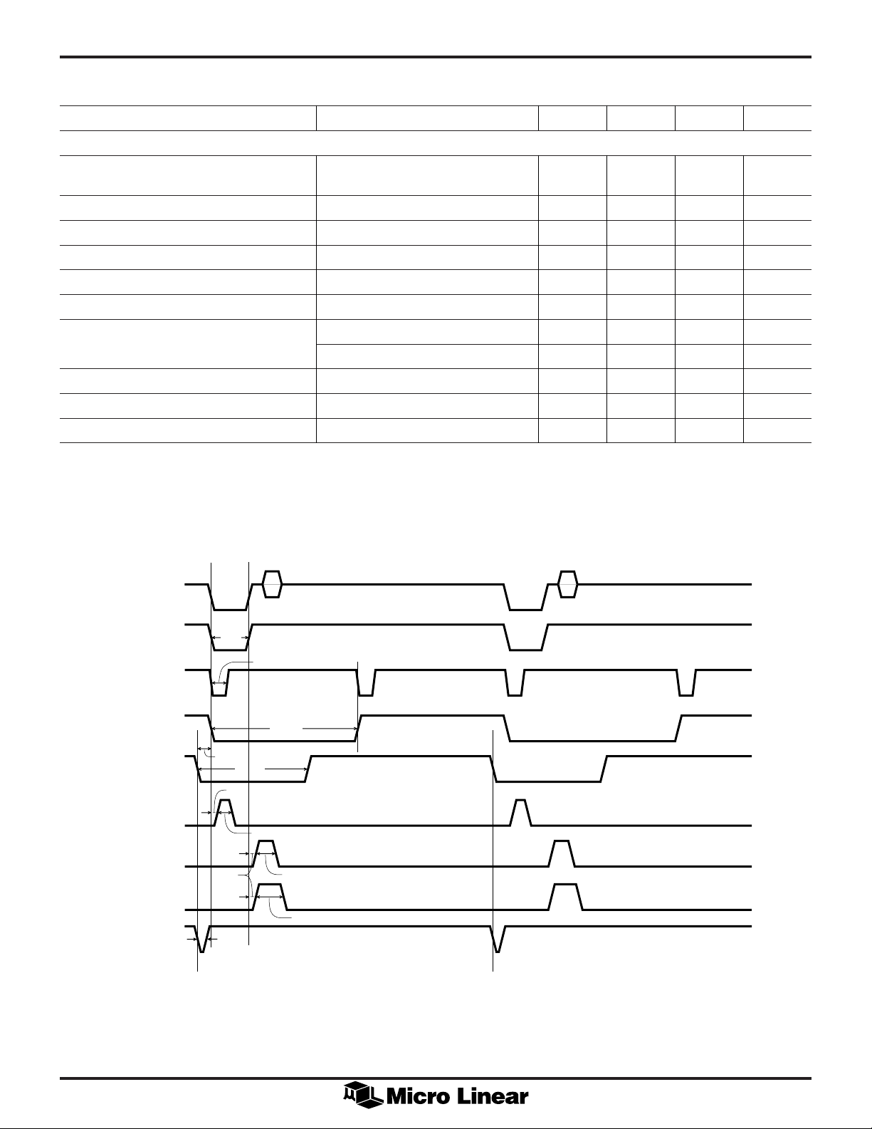
COMPOSITE
REGENERATED
EQUALIZERS
SERRATIONS
CLK
& S
CLK
VIDEO IN
PIN 6
CSYNC
PIN 26
H
BLANK
PIN 25
S
CLAMP
PIN 28
BGATE
PIN 27
B
CLAMP
PIN 27
H
RESET
PIN 23
& S
DATA (tLH
DATA (tHL
DATA (tSU/STOP
t
t
HBLK
t
HBPC
t
HRW
) 30 300 ns
) 30 300 ns
) 0.6 µs
HSW
t
HEQW
t
HSERRW
t
HBLKW
t
HSTC
t
HSTCW
t
HBPGW
t
HBPCW
Figure 1. Line Rate Waveforms
NOTE: NOT TO SCALE
7
Page 8
ML6430/ML6431
DEVICE DIFFERENCES
Tables 1 and 2 summarize the differences between the
ML6430 and ML6431. The pinouts of the ML6430 and the
ML6431 are the same with the exception that the ML6431
DEVICE FUNCTIONAL DESCRIPTION
Video Formats,
Timing, Clock Input Free Run VGA VCR
and Pulse Rates Crystal Mode Clock Lock
Generation
NTSC PAL CCIR601 Square 4xFSC 3.58 4.43
Pixel MHz MHz
ML6430 Yes Yes Yes Yes Yes Yes Yes Yes. Limited Yes. Limited to Yes
ML6431 Yes Yes* Yes Yes* Yes Yes Yes Yes. Faster Yes. Works Yes.
* Readjusted the center frequency for PAL square pixel with NTSC crystal to achieve greater than +/-5% range. See Table 4
has a few enhancements, (Center Frequency and Free Run
Mode, see Table 1) and added functionality (see Table 2).
transition 640x480
between free pixel clock.
run modes
1 and 2.
(Figure 4)
transition be- up to 75MHz.
tween freerun (Table 6)
modes 1and 2.
(Figure 4a)
Table 1. Summary of Functional Differences between the ML6430 and ML6431.
DEVICE MODE REGISTER DIFFERENCES PIN OUT DIFFERENCES
Register 7, Register 7, Pin 3 Pin 16
Bit 2 Bit 3
ML6430 Sleep Mode 0 0 SLEEP AUDIOCLK
Pulse Generator Mode* 1 0 54MHz** AUDIOCLK
Time Base Correction Mode
ML6431 Sleep Mode 0 0 SLEEP AUDIOCLK
Pulse Generator Mode* 1 0 54MHz** AUDIOCLK
PHERROUT Mode* X 1 Must be set HIGH PHERROUT
*For these modes the SLEEP mode can only be enable/disabled via serial bus (Register 8).
**The 54MHz clock input (pin 3) can be any 4 x Clock up to 70MHz
Table 2. Summary of Register Differences between the ML6430 and ML6431.
This function not available in the ML6430
8
Page 9
FUNCTIONAL DESCRIPTION
ML6430/ML6431
DUAL PLLS
The Genlock has the following properties:
• A stable, asynchronous crystal controlled oscillator
provides the basic timing signals.
• A precision analog circuit uses the above timing
signals to generate an arbitrarily phased output whose
phase can be altered at pixel rate.
• A digital PLL loop monitors the error signal from a
digital phase detector, and generates a pixel by pixel
phase adjustment of the output.
• An intelligent state machine further enhances
performance by monitoring errors and error history and
adjusting the gains of the loop accordingly.
• A circuit automatically detects a VCR signal and
increases loop gain for proper tracking and minimum
jitter.
The digital PLL has five operating modes. In normal
operation with a stable input the controller will settle to
state 1. If errors are large and consistent, controller will
move to state 5. If error conditions are corrected,
controller will sequentially decrease the state as the errors
are reduced toward 0. If small but consistent errors persist
while controller is in state 1, then controller may move to
states 2 or 3 to help settle out errors more quickly. None
of these changes will cause a reset of pixel count, or a
discontinuity of output clocks. Operating modes are
described in greater detail below.
1. Normal: Gain is low, instantaneous phase gain is
1/32, giving a net short term jitter gain (output/input
jitter) of about -30db. Full peak to peak jitter (including
lower frequency jitter) from a white source is about 15db.
2. Slow: Gain is increased by 4x, and settling time
reduced by about the same. This mode is used as a
transition mode during normal lock sequence, or as a
modest speed up mode if errors are high.
3. Medium: Gain is increased by 8x, and settling time
reduced by about the same. This mode is used as a
transition mode during normal lock sequence, or as a
speed up mode if errors are consistently high.
4. Fast: Gain is increased by 16x. Adds frequency
adjustments to mode 5 for fast settling during hot
switches or pathological gyro errors in hand held
camcorders.
5. Phase: Only Gain is 16x for phase changes, 0 for
frequency changes. Primarily used to quickly settle
head switch phase errors without affecting loop
frequency.
PHERROUT SIGNAL
The PHERROUT pin indicates, on a line by line basis,
whether the H SYNC pulse of the analog input signal is
leading or trailing the genlock's output H SYNC pulse.
This information is used by the genlock to decide whether
to speed up or slow down the internal clock to achieve
locking of the H SYNC pulses. If PHERROUT = 0, then
the analog sync is ahead; therefore, the internal clock
will speed up in an effort to lock the H SYNC pulses. By
contrast, if PHERROUT = 1, then the analog sync is
behind; therefore, the internal clock will slow down in an
effort to lock the H SYNC pulses. Ultimately, when the
genlock is locked to the incoming analog signal,
PHERROUT will alternate approximately every line
between 0 and 1.
PHERROUT (PIN 16) DESCRIPTION
0 Speed up output timing
1 Slow down output timing
Table 3. PHERROUT Signal Description
SYNC SEPARATION
Sync separation is accomplished using peak tracking
analog amplifiers with a precision sync slicer. The closed
tracking loop is equipped with timers to discriminate true
sync pulses from noise glitches or chroma overshoots. The
use of analog sync separation techniques removes a
serious source of jitter present in most digital PLLs.
CRYSTAL SELECTION
The precision crystal source for the ML6430/ML6431 can
be supplied in one of four ways. An industry standard
3.58MHz parallel tuned NTSC color subcarrier crystal or a
4.43MHz parallel tuned PAL color subcarrier crystal may
be used. Alternately, a 14.318MHz NTSC or 17.7MHz
PAL, 4xFs, or a 3.58MHz or 4.43MHz oscillator source
may be used. Regardless of the crystal used, the ML6430/
ML6431 can lock to PAL, NTSC, Beta or MII or YUV in
either 625 or 525 standards. Table 4 provides the clock
rate accuracy for both the NTSC and PAL clock rates for
each crystal selected. Note that the range may vary
between the ML6430 and the ML6431.
LOW POWER SLEEP MODES
Sleep mode may be initiated either from the serial control
bus, or from an external pin. In both cases the entire chip
except the serial bus is shut down. For applications where
PHERROUT is used, the sleep mode can only be enabled/
disabled via serial control.
9
Page 10
ML6430/ML6431
FUNCTIONAL DESCRIPTION (Continued)
CENTER FREQUENCY AND ± RANGE FOR EACH FREQUENCY
VIDEO STANDARD CLOCK RATE CLOCK RATE
3.58MHz Crystal
NTSC Square Pixel 4xClk= 49.09MHz +8.35%/ –5.19%
NTSC 601 4xClk= 54.00MHz +6.07%/ –7.18%
NTSC 4fsc 4xClk= 57.27MHz +7.15%/ –6.23%
PAL Square Pixel 4xClk= 59.00MHz +4.01%/ –9.10%
PAL 601 4xClk= 54.00MHz +6.07%/–7.18%
PAL 4fsc 4xClk= 35.47MHz +9.58%/ –4.14%
4.43MHz Crystal
NTSC Square Pixel 4xClk= 49.09MHz +8.28%/ –5.23%
NTSC 601 4xClk= 54.00MHz +7.81%/ –5.64%
NTSC 4fsc 4xClk= 57.27MHz +6.00%/ –7.18%
PAL Square Pixel 4xClk= 59.00MHz +7.27%/ –6.13%
PAL 601 4xClk= 54.00MHz +7.81%/–5.64%
PAL 4fsc 4xClk= 35.47MHz +7.05%/ –6.31%
STANDARD OF THE ML6430
ACCURACY
Table 4. NTSC/ PAL Clock Rate Range vs. Crystal Input
DISABLING AUTOMATIC VCR SIGNAL DETECTION
DEVICE DISABLE VCR SIGNAL DETECTION?
ML6430 No. Detection function is always on.
ML6431 Yes. Detection function can be disabled
or enabled via serial bus only. This
feature is enabled by default.
Table 5.
In the ML6430, the VCR detection circuit is always
enabled. This circuit detects the presence of a VCR input
signal at C
VIN
/ H
(pin 6) and automatically adjusts
SYNC
the gain settings for the digital PLL to optimize locking
performance. This circuit scans for head switching greater
than the thresholds selected by the user threshold bits (via
serial bus) and then increases the phase gain of the digital
PLL to compensate.
CENTER FREQUENCY AND ± RANGE FOR EACH FREQUENCY
VIDEO STANDARD CLOCK RATE CLOCK RATE
3.58MHz Crystal
NTSC Square Pixel 4xClk= 49.09MHz +8.35%/ –5.19%
NTSC 601 4xClk= 54.00MHz +6.07%/ –7.18%
NTSC 4fsc 4xClk= 57.27MHz +7.15%/ –6.23%
PAL Square Pixel 4xClk= 59.00MHz +7.47%/ –5.93%
PAL 601 4xClk= 54.00MHz +6.07%/–7.18%
PAL 4fsc 4xClk= 35.47MHz +7.64%/ –5.77%
4.43MHz Crystal
NTSC Square Pixel 4xClk= 49.09MHz +8.28%/ –5.23%
NTSC 601 4xClk= 54.00MHz +7.81%/ –5.64%
NTSC 4fsc 4xClk= 57.27MHz +6.00%/ –7.18%
PAL Square Pixel 4xClk= 59.00MHz +7.27%/ –6.13%
PAL 601 4xClk= 54.00MHz +7.81%/–5.64%
PAL 4fsc 4xClk= 35.47MHz +7.05%/ –6.31%
STANDARD OF THE ML6431
ACCURACY
PULSE GENERATOR MODE
54MHz Input or Any 4X Clock
The 54MHz pin (pin 3) is an input that clocks the
horizontal and vertical counters. In this mode, the
ML6430 or ML6431 is used as a pulse generator. The
input signal at can be any 4X clock; for example, 54MHz
(4 x CCIR clock rate of 13.5MHz), 49.09MHz (4 x Square
Pixel clock rate of 12.27MHz), or 57.27 MHz (4 x Fsc
clock rate of 14.31MHz for NTSC color subcarrier). This
input is limited to 70MHz.
As a pulse generator, the sync, clamp, blanking, and
clock signals are derived from the clock input at the
54MHz pin. This mode is activated by setting the
appropriate values in Register 7 via the serial bus. See
Tables 10 or 11.
USING F
FOR NTSC vs. PAL MODES
RESET
In the ML6431, the VCR detection circuit operates the
same as the ML6430 with the additional ability to disable
or enable the VCR detection circuit to optimize for low
jitter performance. This feature is enabled by default.
This feature can be disabled in the ML6431 only by
setting the appropriate values in Register 7, Bit 0 via the
serial bus interface (see Table 11). When the VCR detect
circuit is disabled, the ML6431 is optimized for low jitter
performance.
10
In NTSC mode, F
(pin 22) goes low on the high-to-
RESET
low transition of the FIELD ID pin (pin 17) and the
beginning of line 1 (see Figure 2).
In the PAL mode, F
(pin 22)goes low on the low-to-
RESET
high transition of the FIELD ID pin and the end of line
310 (see Figure 3).
Page 11

ML6430/ML6431
2
3
4
5
6
7
8
9
10
11
12
13
14
15
16
17
18
19
20
21
22
1
525
263
265264
266
268267
269
271
272
274273
275
277276
278
280279
281
283282
284
262
270
3H
3H 3H
Vertical Blanking Interval
FIELD 1
H
Start of
Field 1
H
H
H/2
H
Vertical Blanking Interval
FIELD 2
Start of
Field 2
H/2
VBLANK
Pin 24
FRESET
Pin 22
FIELDID
Pin 17
9 or 16 Lines
½ Line
FIELDID
Pin 17
(Odd Vertical Intervals Only)
Low For Odd Fields
High For Even Fields
END OF FOURTH FIELD (ODD)
WHITE LEVEL
BLACK LEVEL
BLANKING LEVEL
SYNC LEVEL
END OF FIRST FIELD (EVEN)
WHITE LEVEL
BLACK LEVEL
BLANKING LEVEL
SYNC LEVEL
}
}
622 625624
V
BLANK
Pin 24
F
RESET
Pin 22
ODDFLD
Pin 17
623
EQUALIZING
2.5 LINES
5
PULSES
311310
Figure 2. NTSC Field Rate Waveforms
1
2.5 LINES
FIELD SYNC
5 BROAD
PULSES
312
313
BROAD PULSE
SEPARATION
4.7µs ± 100ns
7.5 or 16 Lines
½ Line
FIELD BLANKING (25 LINES + LINE BLANKING)
BEGINNING OF FIRST FIELD (EVEN)
2
3
EQUALIZING
4
2.5 LINES
5
PULSES
6
5
7
BEGINNING OF SECOND FIELD (ODD)
318
315314
317
316
319
(Second Field Vertical Interval Only)
High for Second Field, Low for First Field
8
9
10
321320
322
12
11
324323
325
14
13
15
327326
328
16
329 336
23
~
~
~
~
Figure 3. PAL 625 Field Rate Waveforms
11
Page 12

ML6430/ML6431
FUNCTIONAL DESCRIPTION (Continued)
FREERUN MODE
Both the ML6430 and ML6431 can be used in Freerun
mode. The ML6431 is recommended for applications
requiring a more robust Freerun mode of operations.
Figure 4 and Figure 4a describe the state diagrams for
both the ML6430 and ML6431. Note that the ML6431
includes a faster path to go from FREERUN MODE #1 to
FREERUN MODE #2.
Freerun mode: FREERUN MODE #1 is entered when
the freerun pin is toggled high while the ML6430/
ML6431 is horizontally locked (i.e. internal horizontal
locked signal is present). In this mode, the digital
frequency value stored in the line-locked PLL is held
and the ML6430/ML6431 will freerun at a frequency
very close to that of the last locked video source.
Freerun mode #1 is best used by physically tying the
NoSignal pin to the freerun pin as shown in Figures 9
or 10. FREERUN MODE #2 is entered when the
freerun pin is toggled high while the ML6430/Ml6431
is not horizontally locked to a video source. In this
mode, a ROM lookup table is used to set the freerun
frequency of the ML6430/ML6431. In this mode the
output frequency is as accurate as the Crystal plus the
accuracy of the look up table. See Figures 4 and 4a
for the NoSignal-Locked-Freerun state machine
diagram.
NoSignal: NoSignal will go low if video is present for
one entire field. NoSignal will be high if video is not
present for one entire field.
Locked (ML6430): The ML6430 must be line
(horizontal) locked to an input video source and also
be vertically locked before the locked detect signal
goes high. When a video source is removed, the
locked signal may be high or low. Please note that the
locked pin is the logical AND of the internal
horizontal locked and vertical locked signals. For
example, the internal horizontal locked signal may be
high even though the locked pin is asserted low.
POWER UP
ML6430 W/
FREERUN PIN
"LOW" (TYPICAL)
INPUT VIDEO
WITHIN ±6%
RANGE
HORIZONTAL
LOCKED
SIGNAL
PRESENT
2
HORIZONTAL
UNLOCKED
SIGNAL
PRESENT
1
IF NO VIDEO
FOR > 1 FRAME
IF INPUT VIDEO
FOR > 1 FRAME
INPUT VIDEO
OUTSIDE ±6%
RANGE
IF NO VIDEO
FOR > 1 FRAME
IF INPUT VIDEO
FOR > 1 FRAME
TOGGLE
FREERUN PIN
"HIGH"
HORIZONTAL
NO SIGNAL
HORIZONTAL
UNLOCKED
NO SIGNAL
TOGGLE
FREERUN PIN
"HIGH"
LOCKED
PRESENT
3
PRESENT
4
TOGGLE
FREERUN PIN
"HIGH"
FREERUN PIN
"LOW"
FREERUN PIN
"LOW"
TOGGLE
FREERUN PIN
"HIGH"
FREERUN
MODE #1
5
FREERUN
MODE #2
6
POWER UP
ML6430 W/
FREERUN PIN
"HIGH" (TYPICAL)
12
Figure 4. ML6430 Freerun Mode State Diagram
Page 13

FUNCTIONAL DESCRIPTION (Continued)
INPUT VIDEO
WITHIN ±6%
RANGE
POWER UP
ML6431 W/
FREERUN PIN
"LOW" (TYPICAL)
POWER UP
ML6431 W/
FREERUN PIN
"HIGH" (TYPICAL)
IF NO VIDEO
FOR > 1 FRAME
TOGGLE
FREERUN PIN
"HIGH"
TOGGLE
FREERUN PIN
"HIGH"
TOGGLE
FREERUN PIN
"HIGH"
IF INPUT VIDEO
FOR > 1 FRAME
FREERUN PIN
"LOW"
IF NO VIDEO
FOR > 1 FRAME
FREERUN PIN
"LOW"
IF INPUT VIDEO
FOR > 1 FRAME
TOGGLE
FREERUN PIN
"HIGH"
INPUT VIDEO
OUTSIDE ±6%
RANGE
IF NO VIDEO
FOR > 2 FRAMES
HORIZONTAL
LOCKED
NO SIGNAL
PRESENT
3
FREERUN
MODE #1
5
HORIZONTAL
LOCKED
SIGNAL
PRESENT
2
HORIZONTAL
UNLOCKED
NO SIGNAL
PRESENT
4
FREERUN
MODE #2
6
HORIZONTAL
UNLOCKED
SIGNAL
PRESENT
1
ML6430/ML6431
Locked (ML6431): The ML6431 must be line
(horizontal) locked to an input video source for at
least two fields and also be vertically locked before
the locked detect signal goes high. When a video
source is removed, the ML6431 will lose horizontal
lock after two entire fields with no video present.
However, vertical lock may be lost before horizontal
lock. Because the locked pin is the logical AND of
the internal horizontal locked and vertical locked
signals the locked pin may go low before the internal
horizontal locked signal.
VGA CLOCKS
For VGA applications the ML6431 is recommended.
Table 6 provides a list of the VGA clocks that can be
generated using the ML6431. To use the information in
Table 6 first find the resolution and refresh rate required.
Determine which crystal, PAL or NTSC is needed. Change
the crystal to the proper frequency if necessary. Over the
serial-bus, program the registers as indicated in Table 6.
Supply to pin 6 an horizontal sync signal at TTL or CMOS
levels and at the specified frequency. Trigger an
oscilloscope on the falling edge of the horizontal input to
view the outputs. The VGA pixel clock will be found on
pin 18. Other useful signals are noted in table 6. External
logic may be needed to produce usable vertical sync
pulses.
AUDIO CLOCKS
The audio modes can be activated via serial bus (Register
7). When this mode is activated an audio clock
frequency can be selected via serial bus (Register 8). See
Table 9.
Figure 4a. ML6431 Freerun Mode State Diagram
13
Page 14

14
ML6430/ML6431
ML6431 Data Register Settings*
Resolution # Pixels Refresh Horizontal Pixel Standard Original Freq. Std. PALXtal Pixel Reg PherrOut VGA External Pixel Horizontal Vertical
per Line Rate Frequency Frequency Type Standard # Xtal Used Clk Output Pulses Pulses
640 x 480 800 60 Hz 31.5 KHz 25.175 MHz Industry NTSC Sq Pix =000 1 572 0 1 4.43 2X “Hsync,Hreset” Vreset
832 72 Hz 37.9 KHz 31.500 MHz VESA VS901101 NTSC Sq Pix =000 0 640 0 1 4.43 2X “Hsync,Hreset” Vreset
840 75 Hz 37.5 KHz 31.500 MHz VESA VDMT75HZ NTSC Sq Pix =000 0 656 0 1 4.43 2X “Hsync,Hreset” Vreset**
800 x 600 1024 56 Hz 35.1 KHz 36.000 MHz VESA VG900601 PAL 4FSC =101 1 512 1 1 4.43 4X “Hsync,Hreset” Vreset
1056 60 Hz 37.9 KHz 40.000 MHz VESA VG900602 NTSC Sq Pix =000 1 544 1 1 3.58 4X “Hsync,Hreset” Vreset**
1040 72 Hz 48.1 KHz 50.000 MHz VESA VS900603A NTSC Sq Pix =000 1 528 1 1 4.43 4X “Hsync,Hreset” Vreset**
1056 75 Hz 46.9 KHz 49.500 MHz VESA VDMT75HZ NTSC Sq Pix =000 1 544 1 1 4.43 4X “Hsync,Hreset” Vreset**
1024 x 768 1264 43 Hz/Int 35.5 KHz 44.900 MHz Industry PAL 4FSC =101 0 752 1 1 4.43 4X “Hsync,Hreset” Vreset**
1344 60 Hz 48.4 KHz 65.000 MHz VESA VG901101A PAL 601 = 011 0 832 1 1 4.43 4X “Hsync,Hreset” Vreset**
1328 70 Hz 56.5 KHz 75.000 MHz VESA VS910801-2 PAL 4FSC =101 0 816 1 1 3.58 4X & clk No No
doubler
*For Data Register Settings: TTL = High, VGA = On, VCR = Off, Noise Gating = On, Dis Auto Ver Det = 1
** w/ external glue logic
Table 6. VGA Rates Supported
Page 15

FUNCTIONAL DESCRIPTION (Continued)
ML6430/ML6431
PRESET PIN CONTROL
The ML6430/ML6431 may be controlled via a set of four
preset mode pins. These pins do not allow access to all
the programmable features of the ML6430/ML6431, but
are intended to provide a simpler interface for most
applications.
P3 P2 P1 P0 STD CLOCK RATE CRYSTAL
0101NTSC Square pixel 3.58MHz
1001NTSC CCIR601 3.58MHz
1101NTSC 4Fsc 3.58MHz
0111PAL Square pixel 3.58MHz
1 0 1 1 PAL CCIR601 3.58MHz
1111PAL 4Fsc 3.58MHz
PULSE OUTPUTS
Pulse outputs are defined in Table 12. Note that the pulse
widths and start times are chosen to the nearest clock
edge, and indicated errors assume nominal clock
operating frequency.
P3 P2 P1 P0 STD CLOCK RATE CRYSTAL
0 Z 0 Z NTSC Square pixel 17.72MHz
Z 0 0 Z NTSC CCIR601 17.72MHz
Z Z 0 Z NTSC 4Fsc 17.72MHz
0 Z 1 Z PAL Square pixel 17.72MHz
Z 0 1 Z PAL CCIR601 17.72MHz
Z Z 1 Z PAL 4Fsc 17.72MHz
010ZNTSC Square pixel 4.43MHz
100ZNTSC CCIR601 4.43MHz
1 1 0 Z NTSC 4Fsc 4.43MHz
0 1 1 Z PAL Square pixel 4.43MHz
101ZPAL CCIR601 4.43MHz
1 1 1 Z PAL 4Fsc 4.43MHz
0 Z 0 1 NTSC Square pixel 14.32MHz
Z 0 0 1 NTSC CCIR601 14.32MHz
Z Z 0 1 NTSC 4Fsc 14.32MHz
0 Z 1 1 PAL Square pixel 14.32MHz
Z 0 1 1 PAL CCIR601 14.32MHz
Z Z 1 1 PAL 4Fsc 14.32MHz
Table 7. Preset Pin Modes
Z 1 0 1 NTSC Square pixel, VGA 3.58MHz
1 Z 0 1 NTSC CCIR601,VGA 3.58MHz
0001NTSC 4Fsc, VGA 3.58MHz
Z 1 1 1 PAL Square pixel, VGA 3.58MHz
1 Z 1 1 PAL CCIR601, VGA 3.58MHz
0011PAL 4Fsc, VGA 3.58MHz
Z 1 0 Z NTSC Square pixel, VGA 4.43MHz
1 Z 0 Z NTSC CCIR601, VGA 4.43MHz
000ZNTSC 4Fsc, VGA 4.43MHz
Z 1 1 Z PAL Square pixel, VGA 4.43MHz
1 Z 1 Z PAL CCIR601, VGA 4.43MHz
001ZPAL 4Fsc, VGA 4.43MHz
XXX0 Serial control mode
Z = Floating input, 0 = Low input, 1 = High input, X = Don’t care
15
Page 16

ML6430/ML6431
FUNCTIONAL DESCRIPTION (Continued)
CONTROL REGISTER INFORMATION
REGISTER SETTING
PulsePol[2:0] 000
Clk4X 0
Pixel[10:0] Determined by PRESET pin
Burst 0
CSyncRaw 0
RawClamp 0
TTL Sync 0
WideBlank 0
HDelay[6:0] 1000000
Noise Gating 0
Test 3,1,4 0, 0, 0
External 54
Clock IN 0
FAud[1:0] 01
VCR 0
SLEEP 0
Thresh[1:0] 11
VGA Determined by PRESET pin
Div4 Determined by PRESET pin
Fstd[2:0] Determined by PRESET pin
PALX
TAL
Determined by PRESET pin
Table 8. Default Control Register Settings for Preset Mode
RawClamp: Controls the source of the S
CLAMP
(sync
clamp) pulse. Pulse is timed relative to incoming sync
edge, or regenerated sync edge.
PALXTAL: Controls the expected crystal frequency at the
oscillator inputs. 0 = NTSC 3.58MHz, or 1 = PAL 4.43MHz.
Thresh1,Thresh0: Selects the pixel error threshold at
which relock is initiated. Values are:
0,0: 2.5 pixels
0,1: 2.5 pixels
1,0: 1.0 pixels
1,1: 4.0 pixels
Noise Gating: Enables a 3/4 line window to lockout any
unwanted horizontal sync pulses.
VGA: Produces non-interlaced progressive scan outputs.
Div4: Controls the prescaler in the M/N loop. High means
that 4Fs external oscillator signals are expected, low
assumes a PAL or NTSC Fs crystal will be used.
VCR: Controls the gain range and locking maneuvers of
the digital loop. Provides better locking to the
unpredictability of VCR headswitches and jitter.
Blanking Width Control: The number of blanked lines in
the vertical interval is programmable to either 9 or 16.
REGISTER DESCRIPTION
SLEEP: Enables or disables sleep mode. When using
serial bus control, ALL registers must be programmed to
their intended state after power up to ensure correct
operation of the ML6430/ML6431.
CSR: Composite sync register bit controls whether
composite sync output is from the sync separator,
(raw C
(regenerated C
) or from the internal pulse generator
SYNC
SYNC
).
Pulse Polarity Control: The active state of output sync
pulses, blanking pulses, or clamp pulses may be
programmed to either 0 or 1 state by use of these bits.
P0:C
pulse output is high active when 1,
SYNC
low active when 0.
P1:H
BLANK
, and V
pulse outputs are high
BLANK
active when 1, low active when 0.
P2:S
CLAMP
and B
pulse outputs are high
CLAMP
active when 1, low active when 0.
Burst: Controls the length of Burst Gate so pulse can be
used for either burst gating in encoder applications or
back porch clamping.
XTAL: external Crystal Control: 0=NTSC 3.58MHz, or
1=PAL 4.43MHz, for both local crystal and external
oscillator mode.
External 54MHz Clock: This mode permits injecting a
54MHz clock (or other 4X clock) directly into the
horizontal pixel counter via the SLEEP pin. All timing
pulses are synchronous to the 54MHz clock (or other 4X
clock).
Serial Bus Control: To place the Ml6430/ML6431 in serial
mode, take P0 (Preset ) to logical '0' or ground. The serial
control system is written to by the external processor in 8bit bytes. Each of these bytes is partitioned into an
address (upper 4 bits of serial byte) and a data register
(lower 4 bits of serial byte). In Table 10, the Register
heading refers to the 4-bit address, and Data Bit refers to a
particular bit in the 4-bit register (Bit0 is LSB).
Pixel: Program all bits to zero to enable default values for
each standard. Otherwise use the following equation:
P[10:0] = 2 ´ (number of pixels per line) – 1024 (1)
Test: All test bits must be programmed to zero.
16
Page 17

FUNCTIONAL DESCRIPTION (Continued)
ML6430/ML6431
Audio Clock: The Ml6430/ML6431 outputs a clock at
32kHz, 44.1kHz, or 48kHz. This clock is locked in
frequency to the basic video clock regardless of the
standard being used. With VCR head switches, the phase
correction required to track the timing is removed from
the audio clock by a patented circuit. This prevents the
audio clock from being modulated by step changes in
video timing. See the Table 9 for the audio clock rates
supported and how they are derived internally.
ADDITIONAL CONTROL REGISTERS (ML6431 ONLY)
DisAutoVCR: Disables the auto VCR detect circuit.
Register 7, Bit 0: DisAutoVCR
PHERROUT: MUX phase error signal onto
AUDIOCLK/PHERROUT pin.
Register 7, Bit 3: PHERROUT enable
This bit controls the source of AUDIOCLK/PHERROUT.
When this bit is low, AUDIOCLK/PHERROUT provides the
audio clock output. When this bit is high, AUDIOCLK/
PHERROUT provides the 1-bit digital phase error of each
Hsync edge.
Additionally, when both PHERROUT enable and VGA bits
are logic high, the reset point of the pixel counter is
changed from 512 to 256. This changes the equation for
calculating the number of pixels per line verses the Pixel
Counter bits to the following:
P[10:0] = 2 ´ (number of pixels per line) – 512 (2)
VIDEO STANDARD AUDIO RATE AUDIO/PIXEL CLOCK RATIO AUDIO/FRAME RATE RATIO
CCIR601 NTSC 48kHz (96000 ÷ 27MHz) ´ 13.5MHz (8008 ÷ 5) ´ 29.97Hz
CCIR601 NTSC 44.1kHz (88200 ÷ 27MHz) ´ 13.5MHz (147147 ÷ 100) ´ 29.97Hz
CCIR601 NTSC 32kHz (64000 ÷ 27MHz) ´ 13.5MHz (16016 ÷ 15) ´ 29.97Hz
CCIR601 PAL 48kHz (96000 ÷ 27MHz) ´ 13.5MHz (1920) ´ 25Hz
CCIR601 PAL 44.1kHz (88200 ÷ 27MHz) ´ 13.5MHz (1764) ´ 25Hz
CCIR601 PAL 32kHz (64000 ÷ 27MHz) ´ 13.5MHz (1280) ´ 25Hz
NTSC Square Pixel 48kHz (105600 ÷ 27MHz) ´ 12.27MHz (8008 ÷ 5) ´ 29.97Hz
NTSC Square Pixel 44.1kHz (97020 ÷ 27MHz) ´ 12.27MHz (147147 ÷ 100) ´ 29.97Hz
NTSC Square Pixel 32kHz (70400 ÷ 27MHz) ´ 12.27MHz (16016 ÷ 15) ´ 29.97Hz
PAL Square Pixel 48kHz (96000 ÷ 29.5MHz) ´ 14.75MHz (1920) ´ 25Hz
PAL Square Pixel 44.1kHz (88200 ÷ 29.5MHz) ´ 14.75MHz (1764) ´ 25Hz
PAL Square Pixel 32kHz (64000 ÷ 29.5MHz) ´ 14.75MHz (1280) ´ 25Hz
NTSC 4xFSC 48kHz (105600 ÷ 31.5MHz) ´ 14.32MHz (8008 ÷ 5) ´ 29.97Hz
NTSC 4xFSC 44.1kHz (92400 ÷ 30MHz) ´ 14.32MHz (147147 ÷ 100) ´ 29.97Hz
NTSC 4xFSC 32kHz (70400 ÷ 31.5MHz) ´ 14.32MHz (16016 ÷ 15) ´ 29.97Hz
PAL 4xFSC 48kHz (76800 ÷ 28.37MHz) ´ 17.72MHz (1920) ´ 25Hz
PAL 4xFSC 44.1kHz (70560 ÷ 28.37MHz) ´ 17.72MHz (1764) ´ 25Hz
PAL 4xFSC 32kHz (51200 ÷ 28.37MHz) ´ 17.72MHz (1280) ´ 25Hz
Table 9. Audio Clock Generation (ML6430/ML6431)
17
Page 18

ML6430/ML6431
REGISTER DATA DESCRIPTION VALUE RANGE BIT CODE
BIT RANGE
0 0 PulsePol 0 C
0 1 PulsePol 1 H/V Blank Polarity High Active-Low Active 0 or 1
0 2 PulsePol 2 S/B Clamp Polarity High Active-Low Active 0 or 1
0 3 Clk 4X Select 4X Clock Low 1X Clock = 13.5MHz 0 or 1
1 0 Pixel0 Pix Counter Load Bit 0
1 1 Pixel1 Pix Counter Load Bit 1
1 2 Pixel2 Pix Counter Load Bit 2
1 3 Pixel3 Pix Counter Load Bit 3
2 0 Pixel4 Pix Counter Load Bit 4
2 1 Pixel5 Pix Counter Load Bit 5
2 2 Pixel6 Pix Counter Load Bit 6
2 3 Pixel7 Pix Counter Load Bit 7
3 0 Pixel8 Pix Counter Load Bit 8
3 1 Pixel9 Pix Counter Load Bit 9
3 2 Pixel10 Pix Counter Load Bit 10
3 3 Burst Burst Gate Enable Low = Back Porch Clamp 0 or 1
Polarity High Active-Low Active 0 or 1
SYNC
High 4X Clock = 54MHz
Numerical value taken as unsigned
binary. Actual no. of pixels is:
nom = ~011 0000 0000
10 0
P:
512
Do not vary pixel [10:0] by more than
±6% from nominal.
1024 > no. of pixels > 512 and
f
NOM
High = Burst Gate
+
x 1.06 > f
2
NEW
> f
NOM
max = 011 0011 0000
min = 010 1101 0000
x 0.94
4 0 CSyncRaw (or C
4 1 RawClamp (or Clamp Regen) Low = regenerated Clamp 0 or 1
4 2 TTL Sync TTL horizontal + vertical Low = sync separator active 0 or 1
Sync Input High = TTL horiz + vert sync input
4 3 WideBlank (or Narrow) Low = narrow blanking 0 or 1
5 0 HDelay0
5 1 HDelay1
5 2 HDelay2
5 3 HDelay3
6 0 HDelay4
6 1 HDelay5
6 2 HDelay6
6 3 Noise Gating 3/4 line lockout Low = noise gating on 0 or 1
H Delay parameter allows
moving the entire constellation
of output pulses relative to the
incoming H
Sync Tip clamp may be
selected for delay or triggered
from incoming sync
depending on application.
Regen) Low = regenerated C
SYNC
. Exception:
SYNC
High = raw C
High = raw Clamp
High = wide blanking
7-bit Horizontal Delay parameter.
Values:
–64p< Hdly < 63p, p = 1/F
High = noise gating off
SYNC
SYNC
4XCLK
0 or 1
0000000 to 1111111:
0000000 means –64p
1111111 means +63p
1000000 means 0p
Table 10. ML6430 Register Map
18
Page 19

ML6430/ML6431
REGISTER DATA DESCRIPTION VALUE RANGE BIT CODE
BIT RANGE
7 0 Test 3 For test mode only:
No user programmable features Set to 0 0
7 1 Test 1 For test mode only:
No user programmable features Set to 0 0
7 2 Ext 54 Low = Pin 3 is SLEEP
Clock IN High = Pin 3 is 54MHz Clock 0 or 1
7 3 Test 4 For test mode only:
No user programmable features Set to 0 0
8 0 FAud0 AudioClk Freq Bit 0 00 = 48kHz, 01 = 44.1kHz, 10 = 32kHz 00 to 10
8 1 FAud1 AudioClk Freq Bit 1
8 2 VCR Enable VCR Mode High = Enabled, Low = Disabled
8 3 SLEEP Power Down Mode High = Power Down, Low = Normal 0 or 1
9 0 Thresh0 Select ‘Out of Lock’ Threshold 00 = 2.5 Pixels 10 = 1.0 Pixels 00 to 11
9 1 Thresh1 01 = 2.5 Pixels 11 = 4.0 Pixels
9 2 VGA Enable VGA Mode High = Enabled, Low = Disabled 0 or 1
9 3 Div4 Enable /4 on M/N Loop High = Enabled, Low = Disabled 0 or 1
10 0 FStd0 Freq Std Sel Bit 0 000 = NTSC Sq Pix 011 = PAL 601 000 to 101
10 1 FStd1 Freq Std Sel Bit 1 001 = PAL Sq Pix 100 = NTSC 4Fsc
10 2 FStd2 Freq Std Sel Bit 2 010 = NTSC 601 101 = PAL 4Fsc
10 3 PALX
TAL
Enable PAL Ref Freq High = Enabled, Low = Disabled 0 or 1
Table 10. ML6430 Register Map (Continued)
19
Page 20

ML6430/ML6431
REGISTER DATA DESCRIPTION VALUE RANGE BIT CODE
BIT RANGE
0 0 PulsePol 0 C
0 1 PulsePol 1 H/V Blank Polarity High Active-Low Active 0 or 1
0 2 PulsePol 2 S/B Clamp Polarity High Active-Low Active 0 or 1
0 3 Clk 4X Select 4X Clock Low 1X Clock = 13.5MHz 0 or 1
1 0 Pixel0 Pix Counter Load Bit 0
1 1 Pixel1 Pix Counter Load Bit 1
1 2 Pixel2 Pix Counter Load Bit 2
1 3 Pixel3 Pix Counter Load Bit 3
2 0 Pixel4 Pix Counter Load Bit 4
2 1 Pixel5 Pix Counter Load Bit 5
2 2 Pixel6 Pix Counter Load Bit 6
2 3 Pixel7 Pix Counter Load Bit 7
3 0 Pixel8 Pix Counter Load Bit 8
3 1 Pixel9 Pix Counter Load Bit 9
3 2 Pixel10 Pix Counter Load Bit 10
3 3 Burst Burst Gate Enable Low = Back Porch Clamp 0 or 1
Polarity High Active-Low Active 0 or 1
SYNC
High 4X Clock = 54MHz
Numerical value taken as unsigned
binary. Actual no. of pixels is:
10 0
P:
+
Do not vary pixel [10:0] by more than
±6% from nominal.
If PHERR enable and VGA = 1, the
actual no. of pixels is:
P[10:0]=2x(no. of pixels per line)–512
High = Burst Gate
512
1024 > no. of pixels > 512 and
f
x 1.06 > f
NOM
2
NEW
> f
NOM
x 0.94
nom = ~011 0000 0000
max = 011 0011 0000
min = 010 1101 0000
4 0 CSyncRaw (or C
4 1 RawClamp (or Clamp Regen) Low = regenerated Clamp 0 or 1
4 2 TTL Sync TTL horizontal + vertical Low = sync separator active 0 or 1
Sync Input High = TTL horiz + vert sync input
4 3 WideBlank (or Narrow) Low = narrow blanking 0 or 1
5 0 HDelay0
5 1 HDelay1
5 2 HDelay2
5 3 HDelay3
6 0 HDelay4
6 1 HDelay5
6 2 HDelay6
6 3 Noise Gating 3/4 line lockout Low = noise gating on 0 or 1
H Delay parameter allows
moving the entire constellation
of output pulses relative to the
incoming H
Sync Tip clamp may be
selected for delay or triggered
from incoming sync
depending on application.
Regen) Low = regenerated C
SYNC
. Exception:
SYNC
High = raw C
High = raw Clamp
High = wide blanking
7-bit Horizontal Delay parameter.
Values:
–64p < Hdly < 63p, p = 1/F
High = noise gating off
SYNC
SYNC
4XCLK
0 or 1
0000000 to 1111111:
0000000 means –64p
1111111 means +63p
1000000 means 0p
Table 11. ML6431 Register Map
20
Page 21

ML6430/ML6431
REGISTER DATA DESCRIPTION VALUE RANGE BIT CODE
BIT RANGE
7 0 DisAutoVCR 0=Auto VCR Detect ON 0 or 1
1=Disable Auto VCR Detect
7 1 Test 1 For test mode only:
No user programmable features. Set to 0 0
7 2 Ext 54 Low = Pin 3 is SLEEP
Clock IN High = Pin 3 is Ext 54MHz Clock 0 or 1
7 3 PHERROUT or AUDIOCLK Low=Pin 16 is Audio CLK, Pin 3 is
SLEEP
High=Pin 16 is PHERROUT, Pin 3
is RESET 0 or 1
8 0 FAud0 AudioClk Freq Bit 0 00 = 48kHz, 01 = 44.1kHz, 10 = 32kHz 00 to 10
8 1 FAud1 AudioClk Freq Bit 1
8 2 VCR Enable VCR Mode High = Enabled, Low = Disabled
8 3 SLEEP Power Down Mode High = Power Down, Low = Normal
9 0 Thresh0 Select ‘Out of Lock’ Threshold 00 = 2.5 Pixels 10 = 1.0 Pixels 00 to 11
9 1 Thresh1 01 = 2.5 Pixels 11 = 4.0 Pixels
9 2 VGA Enable VGA Mode High = Enabled, Low = Disabled 0 or 1
9 3 Div4 Enable /4 on M/N Loop High = Enabled, Low = Disabled 0 or 1
10 0 FStd0 Freq Std Sel Bit 0 000 = NTSC SqPix 011 = PAL 601 000 to 100
10 1 FStd1 Freq Std Sel Bit 1 001 = PAL Sq Pix 100 = NTSC 4Fsc
10 2 FStd2 Freq Std Sel Bit 2 010 = NTSC 601
10 3 PALX
TAL
Enable PAL Ref Freq High = Enabled, Low = Disabled 0 or 1
Table 11. ML6431 Register Map (Continued)
21
Page 22

ML6430/ML6431
FUNCTIONAL DESCRIPTION (Continued)
SERIAL BUS OPERATION
The serial bus control in the ML6430/ML6431 has two
levels of addressing: Device Addressing and Register
Addressing.
Device Addressing: Figure 5 shows the physical
waveforms generated in order to address the ML6430/
ML6431. There are six basic parts of the waveform:
1. Start Indication: Clock Cycle 0
2. Device Address Shifted: Clock Cycle 1 through 8
3. Device Address Strobed and Decoded: Clock Cycle 9
START
S
DATA
t
t
SET/START
RISE
All Other S
Transitions Must Occur While S
DATA
4. Data Shifted : Clock Cycle 10 through 17
5. Data Strobed into Appropriate Register: Clock Cycle 18
6. Stop indication: Clock Cycle 19
Register Addressing: Figure 6 shows the register map of
the ML6430/6431. There are two basic parts of each
received data byte: Address Nibble and Data Nibble
1. Address Nibble: The upper 4 bits of the data byte
gives the register number in which to place the
data.
2. Data Nibble: The lower 4 bits of the data byte is
the data to be placed in the currently addressed
register nibble.
t
CLK
is Low
FALL
S
CLK
START: A Falling Edge on the S
STOP: A Rising Edge on the S
DATA
DATA
While S
While S
is Held High
CLK
is Held High
CLK
Figure 5. Definition of START & STOP on Serial Data Bus
S
S
DATA
CLK
MSB MSB
A1 A0A6A7
0 1 2 7 8 9 10 11 16 17 18
S
:
9th pulse strobes address decoder
CLK
S
:
Rising edge enables data transfer
CLK
S
Value set to A6, Device Address (MSB-1)
:
DATA
Falling edge disables data transfer
S
:
CLK
Rising edge enables data transfer
S
:
CLK
Value set to A7, Device Address MSB
S
:
DATA
Falling edge in prep for first address transfer
S
:
CLK
Falling edge with S
S
DATA
;
Hi means start of sequence
CLK
D7 D6 D1 D0
S
DATA
S
DATA
S
CLK
S
CLK
S
DATA
S
CLK
S
CLK
S
DATA
STOP
:
Rising edge with S
Value set low in prep for STOP
:
18th pulse strobes data shift register
:
Rising edge enables data transfer
:
Value set to D6, Data MSB-1
:
Falling edge disables data transfer
:
Rising edge enables data transfer
:
Value set to D7, Data MSB
:
Hi = STOP
CLK
STOP
22
Figure 6. Definition of DATA FORMAT on Serial Data Bus
Page 23

S
DATA
ML6430/ML6431
STROBE
‘1’ ‘0’ ‘0’ ‘0’ Ø ØR3 R2 R1 R0 D3 D2 D1 D0‘0’‘1’ ‘1’ ‘1’
S
CLK
0 1 234 5 9ABCD EFGH
DEVICE ADDR = ‘B2’ DATAREGISTER
687
S
:
Address decode strobed on 9th clock
CLK
[Data is ‘don’t care’ during strobe]
‘1011 0010’ shifted on next 8 clocks
:
S
DATA
Falling edge in prep for device address transfer
S
:
CLK
SUB-ADDR
S
Final Clock strobes data into register
:
DATA
Second 4 bits are Register Data
S
:
DATA
First 4 bits are Register Address
S
:
DATA
Figure 7. Typical Serial Bus Command
S
DATA
0110010 11101 000
1
I
S
CLK
START
1
23456789ABCDEF
Register Address
Device Address
Strobe in Address
Figure 8. Serial Bus Command to Set Bit #2 in Register 7
GH
Data
Data Strobed into
Appropriate Register
ISTOP
23
Page 24

ML6430/ML6431
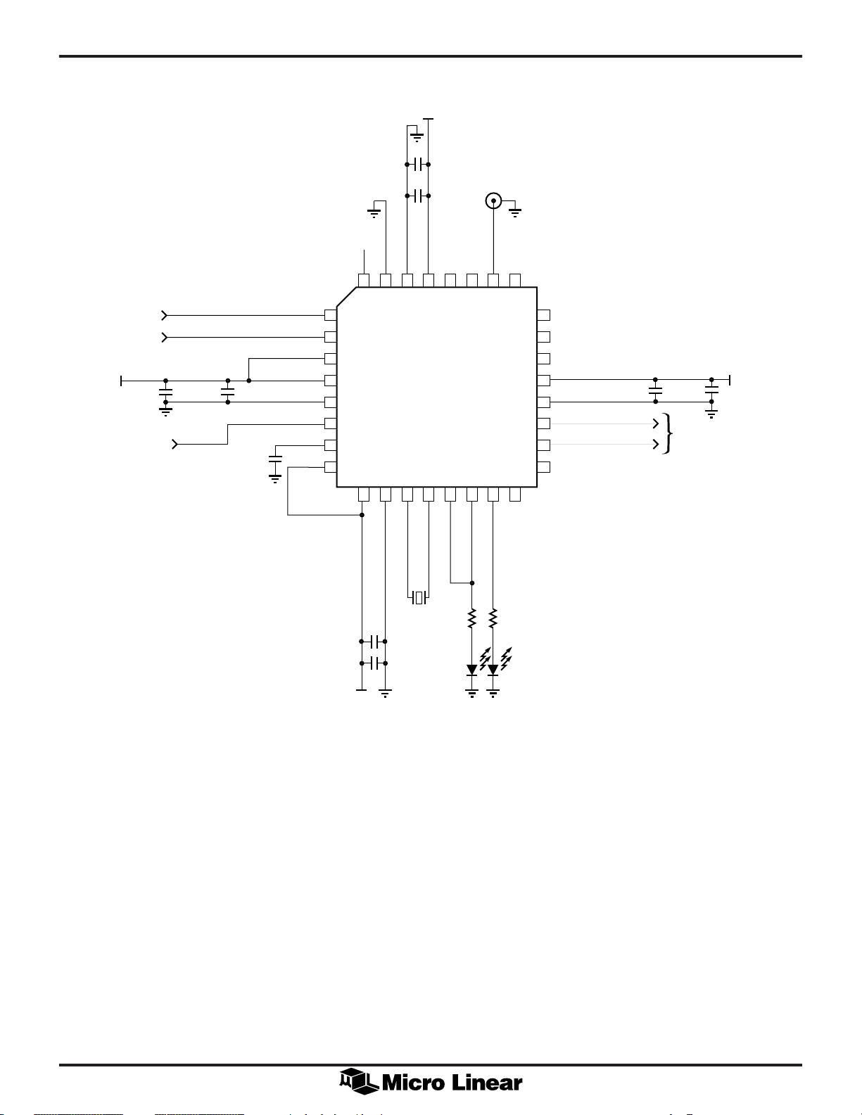
APPLICATIONS
The ML6430 and ML6431 can be used for a variety of
applications. The following figures provide a basic setup
for the various applications listed below:
Figure 9: ML6430 or ML6431 in NTSC CCIR Applications
Figure 10: ML6430 or ML6431 in PAL CCIR Applications
Figure 11: ML6431 in VGA Application
Figure 12: ML6430 or ML6431 in Audio Applications
Figure 13: ML6430 or ML6431 in Pulse Generator
Applications
24
Page 25

5V
ML6430/ML6431
5V
0.1µF
CV in
5V
0.001µF
1.0µF
SLEEP/54MHz
C
1.0µF
75Ω
5V for 3.54 MHz XTAL or
open for 4.43 MHz XTAL
32 31 30 29 28 27 26 25
CC
CLK
REF
1
2
3
4
S
5
6
7
8
9 10111213141516
P2/S
DATA
P3/S
V
GND S
VIN/HSYNC
CV
V
SYNC
1.0µF
0.1µF
D
P1
P0
GND D
V
CC
ML6430/ML6431
GND A
IN
XTAL
OUT
XTAL
A
CC
V
CV
CLAMP/BURST
CLAMP
S
B
FREERUN
NOSIGNAL
SYNCH
SYNC
C
LOCKED
OUT
BLANK
H
24
V
BLANK
23
H
RESET
22
F
RESET
21
VCC B
20
GND B
19
1X CLOCK/4X CLOCK
18
2X CLOCK
17
FIELD ID
0.1µF
1nF
5V
3.58MHz
or 4.43MHz
1nF
0.1µF
5V
Note 1. For minimum V
*PHERROUT is only available with the ML6431
bypassing, connect capacitors VCCA only. (VCCA to GND A)
CC
AUDIOCLK/PHERROUT*
410400
5V LED5V LED
Figure 9. ML6430/ML6431 in NTSC CCIR Applications Programmed via Preset Pins
25
Page 26

ML6430/ML6431
5V
+5V
0.1µF
CV in
5V
0.001µF
1.0µF
SLEEP/54MHz
C
1.0µF
75Ω
5V for 3.54 MHz XTAL or
open for 4.43 MHz XTAL
5V
32 31 30 29 28 27 26 25
CLK
REF
1
2
3
4
S
5
6
7
8
9 10111213141516
P2/S
DATA
P3/S
V
CC
GND S
VIN/HSYNC
CV
V
SYNC
1.0µF
CLAMP
S
CV
B
0.1µF
D
P1
P0
GND D
V
CC
ML6431
GND A
IN
XTAL
OUT
XTAL
FREERUN
NOSIGNAL
A
CC
V
OUT
SYNCH
BLANK
SYNC
CLAMP/BURST
C
H
24
23
22
21
20
19
18
17
LOCKED
V
BLANK
H
RESET
F
RESET
VCC B
GND B
1X CLOCK/4X CLOCK
2X CLOCK
FIELD ID
0.1µF
1nF
5V
3.58MHz
or 4.43MHz
1nF
0.1µF
5V
Note 1. For minimum V
*PHERROUT is only available with the ML6431
bypassing, connect capacitors VCCA only. (VCCA to GND A)
CC
AUDIOCLK/PHERROUT*
410400
5V LED5V LED
Figure 10. ML6430/ML6431 in PAL CCIR Applications Programmed via Preset Pins
26
Page 27
5V
1.0µF
0.1µF
CV
SYNCH
ML6430/ML6431
OUT
5V
H
SYNC
S
DATA
S
0.1µF
CLK
OR CV
0.001µF
SLEEP/54MHz
C
1.0µF
P2/S
DATA
P3/S
CLK
V
CC
GND S
VIN/HSYNC
CV
REF
V
SYNC
D
P1
P0
32 31 30 29 28 27 26 25
1
2
3
4
S
5
6
7
8
9 10111213141516
A
CC
V
GND A
or 4.43MHz
1nF
0.1µF
5V
GND D
ML6431
IN
XTAL
3.58MHz
CC
V
OUT
XTAL
CLAMP/BURST
CLAMP
S
B
FREERUN
NOSIGNAL
BLANK
SYNC
C
H
24
V
BLANK
23
H
RESET
22
F
RESET
21
VCC B
20
GND B
19
1X CLOCK/4X CLOCK
18
2X CLOCK
17
FIELD ID
LOCKED
AUDIOCLK/PHERROUT*
410400
5V LED5V LED
0.1µF
1nF
PIXEL CLOCK
OUTPUT
5V
Note 1. For minimum V
*PHERROUT is only available with the ML6431
bypassing, connect capacitors VCCA only. (VCCA to GND A)
CC
Figure 11. ML6431 in VGA Applications
27
Page 28

ML6430/ML6431
5V
1.0µF
0.1µF
CV
SYNCH
OUT
5V
S
DATA
S
0.1µF
CLK
0.001µF
CV in
1.0µF
SLEEP/54MHz
C
1.0µF
75Ω
P2/S
DATA
P3/S
CLK
V
CC
GND S
VIN/HSYNC
CV
REF
V
SYNC
D
P1
P0
32 31 30 29 28 27 26 25
1
2
3
4
S
ML6430/ML6431
5
6
7
8
9 10111213141516
A
CC
V
GND A
or 4.43 MHz
1nF
0.1µF
5V
GND D
IN
XTAL
3.58MHz
CC
V
OUT
XTAL
CLAMP
S
FREERUN
400
CLAMP/BURST
B
NOSIGNAL
BLANK
SYNC
C
H
24
V
BLANK
23
H
RESET
22
F
RESET
21
VCC B
20
GND B
19
1X CLOCK/4X CLOCK
18
2X CLOCK
17
FIELD ID
LOCKED
AUDIOCLK/PHERROUT*
410
5V LED5V LED
AUDIO CLOCK OUT
0.1µF
1nF
5V
28
Note 1. For minimum V
Note 2. See Table 4 for audio clock frequencies and registers
*PHERROUT is only available with the ML6431
bypassing, connect capacitors VCCA only. (VCCA to GND A)
CC
Figure 12. ML6430/ML6431 in Audio Applications
Page 29

5V
NO
INPUT NEEDED
0.1µF
0.001µF
CV in
1.0µF
See Table 7
for Available
Standards
P2/S
SLEEP/54MHz
C
VIN/HSYNC
1.0µF
75Ω
DATA
P3/S
V
CC
GND S
CV
V
SYNC
CLK
REF
ML6430/ML6431
5V
1.0µF
CV
OUT
CLAMP/BURST
CLAMP
S
B
FREERUN
NOSIGNAL
SYNCH
SYNC
C
LOCKED
BLANK
H
24
V
BLANK
23
H
RESET
22
F
RESET
21
VCC B
20
GND B
19
1X CLOCK/4X CLOCK
18
2X CLOCK
17
FIELD ID
0.1µF
1nF
5V
0.1µF
D
P1
P0
32 31 30 29 28 27 26 25
1
2
3
4
S
ML6430/ML6431
5
6
7
8
9 10111213141516
A
CC
V
GND A
CC
GND D
V
IN
XTAL
XTAL
OUT
3.58MHz
or 4.43 MHz
1nF
0.1µF
5V
Note 1. For minimum V
Note 2. See Table 4 for audio clock frequencies and registers
*PHERROUT is only available with the ML6431
bypassing, connect capacitors VCCA only. (VCCA to GND A)
CC
400
AUDIOCLK/PHERROUT*
410
5V LED5V LED
AUDIO CLOCK OUT
Figure 13. ML6430/ML6431 in Pulse Generator Applications
29
Page 30
ML6430/ML6431
NTSC AT SQUARE PIXEL RATE
SYMBOL NAME: CCIR 601STD TYP UNITS
DESCRIPTION
N
HA
N
H
N
VA
N
V
N
VBLKW
N
VBLKN
t
H
t
HS
t
HSW
Clocks per H: 640 648 cycles
Active
Clocks per H: 780 780 cycles
Whole Line
H per Frame: 486 493,507 lines
Active
H per Frame: 525 525 lines
Whole Line
Lines of Blanking: 16 15 lines
Wide
Lines of Blanking: 9 9 lines
Narrow
H Line Time 63.55 63.55 µs
H Sync Time 0.0 0.0 µs
H Sync Width 4.7 4.73 µs
PAL AT SQUARE PIXEL RATE
SYMBOL NAME: CCIR 601STD TYP UNITS
DESCRIPTION
N
HA
N
H
N
VA
N
V
N
VBLKW
N
VBLKN
t
H
t
HS
t
HSW
Clocks per H: 768 767 cycles
Active
Clocks per H: 944 944 cycles
Whole Line
H per Frame: 609, 616 lines
Active
H per Frame: 625 625 lines
Whole Line
Lines of Blanking: 15 lines
Wide
Lines of Blanking: 9 lines
Narrow
H Line Time 64.0 64.0 µs
H Sync Time 0.0 0.0 µs
H Sync Width 4.7 4.68 µs
t
HRW
t
HEQW
t
HSERRW
t
HSTC
t
HSTCW
t
HBPC
t
HBPGW
t
HBPCW
t
HBLK
t
HBLKW
H Reset Width 41 µs
Equalizer Sync 2.35 2.28 µs
Width
Serration Sync 27.05 µs
Width
Sync Tip Clamp 300 122 ns
Pulse
Sync Tip Clamp 1.5 1.47 µs
Width
BurstPulse 300 326 ns
BurstWidth 2.51 2.44 µs
B Clamp Width 4.0 3.91 µs
H Blanking Pulse –1.5 –1.39 µs
H Blanking Pulse 10.9 10.76 µs
Width
Table 12. Pulse Output Timing
t
HRW
t
HEQW
t
HSERRW
t
HSTC
t
HSTCW
t
HBPC
t
HBPGW
t
HBPCW
t
HBLK
t
HBLKW
H Reset Width 34 µs
Equalizer Sync 2.35 2.31 µs
Width
Serration Sync 27.3 27.32 µs
Width
Sync Tip Clamp 300 102 ns
Pulse
Sync Tip Clamp 1.5 1.49 µs
Width
BurstPulse 300 339 ns
BurstWidth 2.43 2.44 µs
B Clamp Width 4.0 4.0 µs
H Blanking Pulse –1.5 –1.49 µs
H Blanking Pulse 12.0 12.0 µs
Width
30
Page 31

ML6430/ML6431
NTSC AT 4 X FS RATE
SYMBOL NAME: CCIR 601STD TYP UNITS
DESCRIPTION
N
HA
N
H
N
VA
N
V
N
VBLKW
N
VBLKN
t
H
t
HS
t
HSW
Clocks per H: 768 752 cycles
Active
Clocks per H: 910 910 cycles
Whole Line
H per Frame: 486 493,507 lines
Active
H per Frame: 525 525 lines
Whole Line
Lines of Blanking: 16 15 lines
Wide
Lines of Blanking: 9 9 lines
Narrow
H Line Time 63.55 63.55 µs
H Sync Time 0.0 0.0 µs
H Sync Width 4.7 4.68 µs
PAL AT 4 X FS RATE
SYMBOL NAME: CCIR 601STD TYP UNITS
DESCRIPTION
N
HA
N
H
N
VA
N
V
N
VBLKW
N
VBLKN
t
H
t
HS
t
HSW
Clocks per H: 922 922 cycles
Active
Clocks per H: 1135.0064 1135 cycles
Whole Line
H per Frame: 609, 616 lines
Active
H per Frame: 625 625 lines
Whole Line
Lines of Blanking: 15 lines
Wide
Lines of Blanking: 9 lines
Narrow
H Line Time 64.0 64.0 µs
H Sync Time 0.0 0.0 µs
H Sync Width 4.7 4.74 µs
t
HRW
t
HEQW
t
HSERRW
t
HSTC
t
HSTCW
t
HBPC
t
HBPGW
t
HBPCW
t
HBLK
t
HBLKW
H Reset Width 35 µs
Equalizer Sync 2.35 2.30 µs
Width
Serration Sync 27.05 27.02 µs
Width
Sync Tip Clamp 300 105 ns
Pulse
Sync Tip Clamp 1.5 1.47 µs
Width
BurstPulse 300 349 ns
BurstWidth 2.51 2.51 µs
B Clamp Width 4.0 3.98 µs
H Blanking Pulse –1.5 –1.54 µs
H Blanking Pulse 10.9 11.03 µs
Width
Table 12. Pulse Output Timing (Continued)
t
HRW
t
HEQW
t
HSERRW
t
HSTC
t
HSTCW
t
HBPC
t
HBPGW
t
HBPCW
t
HBLK
t
HBLKW
H Reset Width 28 µs
Equalizer Sync 2.35 2.25 µs
Width
Serration Sync 27.3 27.29 µs
Width
Sync Tip Clamp 300 169 ns
Pulse
Sync Tip Clamp 1.5 1.58 µs
Width
BurstPulse 300 225 ns
BurstWidth 2.43 2.48 µs
B Clamp Width 4.0 4.06 µs
H Blanking Pulse –1.5 –1.52 µs
H Blanking Pulse 12.0 12.12 µs
Width
31
Page 32

ML6430/ML6431
NTSC AT CCIR601 RATE
SYMBOL NAME: CCIR 601STD TYP UNITS
DESCRIPTION
N
HA
N
H
N
VA
N
V
N
VBLKW
N
VBLKN
t
H
t
HS
t
HSW
Clocks per H: 720 709 cycles
Active
Clocks per H: 858 858 cycles
Whole Line
H per Frame: 486 493, 507 lines
Active
H per Frame: 525 525 lines
Whole Line
Lines of Blanking: 16 15 lines
Wide
Lines of Blanking: 9 9 lines
Narrow
H Line Time 63.55 63.55 µs
H Sync Time 0.0 0.0 µs
H Sync Width 4.7 4.67 µs
PAL AT CCIR601 RATE
SYMBOL NAME: CCIR 601STD TYP UNITS
DESCRIPTION
N
HA
N
H
N
VA
N
V
N
VBLKW
N
VBLKN
t
H
t
HS
t
HSW
Clocks per H: 720 702 cycles
Active
Clocks per H: 864 864 cycles
Whole Line
H per Frame: 609, 616 lines
Active
H per Frame: 625 625 lines
Whole Line
Lines of Blanking: 15 lines
Wide
Lines of Blanking: 9 lines
Narrow
H Line Time 64.0 64.0 µs
H Sync Time 0.0 0.0 µs
H Sync Width 4.7 4.67 µs
t
HRW
t
HEQW
t
HSERRW
t
HSTC
t
HSTCW
t
HBPC
t
HBPGW
t
HBPCW
t
HBLK
t
HBLKW
H Reset Width 37 µs
Equalizer Sync 2.35 2.37 µs
Width
Serration Sync 27.05 27.04 µs
Width
Sync Tip Clamp 300 111 ns
Pulse
Sync Tip Clamp 1.5 1.48 µs
Width
BurstPulse 300 370 ns
BurstWidth 2.51 2.44 µs
B Clamp Width 4.0 4.10 µs
H Blanking Pulse –1.5 –1.55 µs
H Blanking Pulse 10.9 11.03 µs
Width
Table 12. Pulse Output Timing (Continued)
t
HRW
t
HEQW
t
HSERRW
t
HSTC
t
HSTCW
t
HBPC
t
HBPGW
t
HBPCW
t
HBLK
t
HBLKW
H Reset Width 37 µs
Equalizer Sync 2.35 2.30 µs
Width
Serration Sync 27.30 27.33 µs
Width
Sync Tip Clamp 300 111 ns
Pulse
Sync Tip Clamp 1.5 1.48 µs
Width
BurstPulse 300 370 ns
BurstWidth 2.43 2.44 µs
B Clamp Width 4.0 4.0 µs
H Blanking Pulse –1.5 –1.48 µs
H Blanking Pulse 12.0 12.0 µs
Width
32
Page 33

PHYSICAL DIMENSIONS inches (millimeters)
(
)
Package: H32-7
32-Pin (7 x 7 x 1mm) TQFP
0.354 BSC
(9.00 BSC)
0.276 BSC
(7.00 BSC)
1
PIN 1 ID
25
ML6430/ML6431
0º - 8º
0.003 - 0.008
(0.09 - 0.20)
0.354 BSC
(9.00 BSC)
0.037 - 0.041
0.048 MAX
(1.20 MAX)
0.95 - 1.05
0.018 - 0.030
(0.45 - 0.75)
SEATING PLANE
9
0.032 BSC
(0.8 BSC)
0.276 BSC
(7.00 BSC)
17
0.012 - 0.018
(0.29 - 0.45)
ORDERING INFORMATION
PART NUMBER TEMPERATURE RANGE PACKAGE
ML6430CH 0°C to 70°C 32-Pin TQFP (H32-7)
ML6431CH (EOL) 0°C to 70°C 32-Pin TQFP (H32-7)
© Micro Linear 2000. is a registered trademark of Micro Linear Corporation. All other trademarks are the
property of their respective owners.
Products described herein may be covered by one or more of the following U.S. patents: 4,897,611; 4,964,026; 5,027,116;
5,281,862; 5,283,483; 5,418,502; 5,508,570; 5,510,727; 5,523,940; 5,546,017; 5,559,470; 5,565,761; 5,592,128; 5,594,376;
5,652,479; 5,661,427; 5,663,874; 5,672,959; 5,689,167; 5,714,897; 5,717,798; 5,742,151; 5,747,977; 5,754,012; 5,757,174;
5,767,653; 5,777,514; 5,793,168; 5,798,635; 5,804,950; 5,808,455; 5,811,999; 5,818,207; 5,818,669; 5,825,165; 5,825,223;
5,838,723; 5.844,378; 5,844,941. Japan: 2,598,946; 2,619,299; 2,704,176; 2,821,714. Other patents are pending.
Micro Linear makes no representations or warranties with respect to the accuracy, utility, or completeness of the contents
of this publication and reserves the right to make changes to specifications and product descriptions at any time without
notice. No license, express or implied, by estoppel or otherwise, to any patents or other intellectual property rights is granted
by this document. The circuits contained in this document are offered as possible applications only. Particular uses or
applications may invalidate some of the specifications and/or product descriptions contained herein. The customer is urged
to perform its own engineering review before deciding on a particular application. Micro Linear assumes no liability
whatsoever, and disclaims any express or implied warranty, relating to sale and/or use of Micro Linear products including
liability or warranties relating to merchantability, fitness for a particular purpose, or infringement of any intellectual property
right. Micro Linear products are not designed for use in medical, life saving, or life sustaining applications.
2092 Concourse Drive
San Jose, CA 95131
Tel: 408/433-5200
Fax: 408/432-0295
www.microlinear.com
DS6430_31-01
33
 Loading...