

Datasheet ML6421CS-4, ML6421CS-5, ML6421CS-7, ML6421CS-1, ML6421CS-3 Datasheet (Micro Linear Corporation)
Page 1
September 1999
ML6421*
Triple Phase and Sinx/x Equalized,
Low-Pass Video Filter
GENERAL DESCRIPTION
The ML6421 monolithic BiCMOS 6th-order filter provides
fixed frequency low pass filtering for video applications.
This triple phase-equalized filter with Sinx/x correction is
designed for reconstruction filtering at the output of a
Video DAC.
Cut-off frequencies are either 5.5, 8.0, or 3.0MHz. Each
FEATURES
■ 5.5, 8.0, 9.3, or 3.0MHz bandwidth
■ 1x or 2x gain
■ 6th-order filter with phase and amplitude equalizer
■ >40dB stopband rejection
■ No external components or clocks
channel incorporates a 6th-order lowpass filter, a first
order all-pass filter, a gain boost circuit, and a 75Ω coax
cable driver. A control pin (Range) is provided to allow
the inputs to swing from 0 to 1V, or 0.5 to 1.5V, by
■ ±10% frequency accuracy over maximum supply
and temperature variation
■ <2% differential gain <2° differential phase
providing a 0.5V offset to the input.
■ <25ns group delay variation
The unity gain filters are powered from a single 5V supply,
and can drive 1V
over 75Ω (0.5V to 1.5V), or 2V
P-P
P-P
over 150Ω (0.5V to 2.5V) with the internal coax drivers.
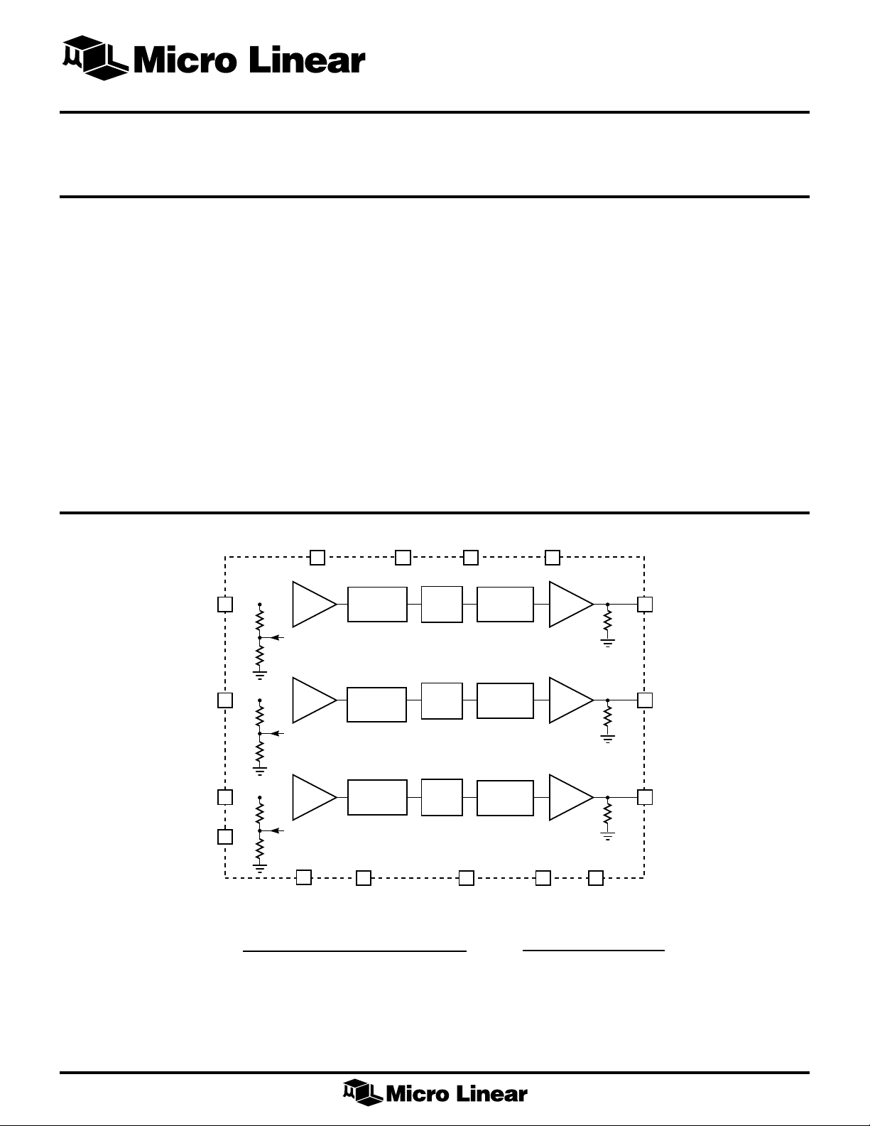
BLOCK DIAGRAM *Some Packages Are Obsolete
15
V
A
IN
3kΩ
1kΩ
I
BIAS
BUF
V
B
CC
8
LOW PASS
FILTER A
C
V
CC
6
■ Drives 1V
P-P
■ 5V ±10% operation
V
CC
5
ALL
PASS
FILTER
SINX/X
EQUALIZER
into 75Ω, or 2V
V
A
CC
11
1X/2X
BUF
3.33kΩ
into 150Ω
P-P
10
V
OUT
A
V
IN
V
IN
RANGE
B
16
3kΩ
1kΩ
2
C
3kΩ
14
1kΩ
I
I
BIAS
BIAS
BUF
BUF
12
GND
LOW PASS
FILTER B
LOW PASS
FILTER C
13
GNDA
ALL
PASS
FILTER
ALL
PASS
FILTER
4
GNDC
SINX/X
EQUALIZER
SINX/X
EQUALIZER
1
GNDB
1X/2X
BUF
1X/2X
BUF
9
3.33kΩ
7
3.33kΩ
3
GND
1x GAIN 2x GAIN
ML6221-1 ML6421-3 ML6421-4 ML6421-5 ML6421-7
FilterA 5.5MHz 8.0MHz 8.0MHz 5.5MHz 9.3MHz
Filter B 5.5MHz 8.0MHz 3.0MHz 5.5MHz 9.3MHz
Filter C 5.5MHz 8.0MHz 3.0MHz 5.5MHz 9.3MHz
Triple Input/Anti-aliasing Video Filter
V
B
OUT
C
V
OUT
1
Page 2
ML6421
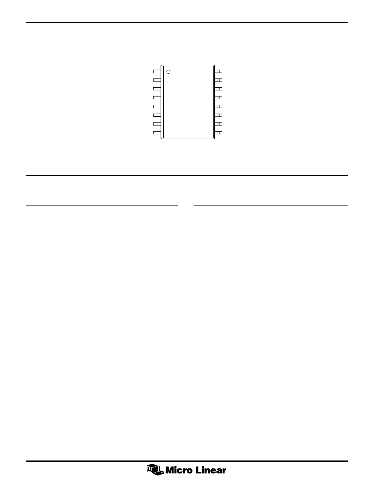
PIN CONFIGURATION
PIN DESCRIPTION
ML6421
16-Pin Wide SOIC (S16W)
CC
1
2
3
4
5
6
7
C
8
TOP VIEW
GNDB
VINC
GND
GNDC
VCCC
V
OUT
VCCB
V
16
VINB
15
VINB
14
RANGE
13
GNDA
12
GND
11
VCCA
10
V
A
OUT
9
V
A
OUT
PIN NAME FUNCTION
1 GNDB Ground pin for filter B.
2VINC Signal input to filter C. Input
impedance is 4kΩ.
3 G N D Po wer and logic ground.
4 GNDC Ground pin for filter C.
5V
CC
Positive supply.
6VCCC Power supply for filter C.
7V
C Output of filter C. Drive is 1V
OUT
75Ω (0.5V to 1.5V), or 2V
P-P
P-P
into
into
150Ω (0.5V to 2.5V).
8VCCB Power supply for filter B: 4.5V to 5.5V.
9V
B Output of filter B. Drive is 1V
OUT
75Ω (0.5V to 1.5V), or 2V
P-P
P-P
into
into
150Ω (0.5V to 2.5V).
10 V
A Output of filter A. Drive is 1V
OUT
75Ω (0.5V to 1.5V), or 2V
P-P
P-P
into
into
150Ω (0.5V to 2.5V).
PIN NAME FUNCTION
11 VCCA Power supply for filter A.
1 2 GN D Power and logic ground.
1 3 GN DA Ground pin for filter A.
14 RANGE Input signal range select.
For –1 to –4; when RANGE is low (0),
the input signal range is 0.5V to 2.5V,
with an output range of 0.5V to 2.5V.
When RANGE is high (1), the input
signal range is 0V to 2V, with an
output range of 0.5V to 2.5V.
For –5 to –7; when RANGE is low (0),
the input signal range is 0.5V to 1.5V,
with an output range of 0.5V to 2.5V.
When RANGE is high (1), the input
signal range is 0V to 1V, with an
output range of 0.5V to 2.5V.
15 VINA Signal input to filter A. Input
impedance is 4kΩ.
16 VINB Signal input to filter B. Input
impedance is 4kΩ.
2
Page 3
ABSOLUTE MAXIMUM RATINGS
ML6421
Absolute maximum ratings are those values beyond which
the device could be permanently damaged. Absolute
maximum ratings are stress ratings only and functional
Package Dissipation at TA = 25°C .............................. 1W
Lead Temperature (Soldering 10 sec) ......................260°C
Thermal Resistance (θJA)..................................... 65°C/W
device operation is not implied.
Supply Voltage (VCC)....................... –5.5MHz0.3 to +7V
GND .................................................. –0.3 to VCC +0.3V
OPERATING CONDITIONS
Logic Inputs ........................................–0.3 to VCC +0.3V
Input Current per Pin ............................................±25mA
Storage Temper ature.................................. –65° to 150°C
TSupply V oltage ...............................................5V ± 10%
Temperature Range ................................ 0°C < to < 70°C
ELECTRICAL CHARACTERISTICS
Unless otherwise specified VCC = 5V ± 10% and TA = T
V
= 1V
OUT
SYMBOL PARAMETER CONDITIONS MIN TYP MAX UNITS
GENERAL
R
IN
DR/R
IN
I
BIAS
for 75Ω Load (Note 1)
P-P
Input Impedance 3 4 5 kΩ
Input R Matching ±2 %
Input Current VIN = 0.5V, ML6421(–1 to –4) –80 µA
range = low ML6421(–5 to –7) 45 µA
VIN = 0.0V, ML6421(–1 to –4) –125 µA
MIN
to T
, RL =75Ω or 150Ω, V
MAX
OUT
= 2V
for 150Ω Load and
P-P
range = high ML6421(–5 to –7) –210 µA
Small Signal Gain VIN = 100mV
at 100kHz ML6421(–5 to –7) 5.5 6 6.5 dB
Differential Gain VIN = 1.1V to 2.5V ML6421(–1 to –4) 1 %
at 3.58 & 4.43 MHz
V
= 0.8V to 1.5V ML6421(–5 to –7) 1 %
IN
at 3.58 & 4.43 MHz
Differential Phase V
V
Input Range Range = 0 ML6421(–1 to –4) 0.5 2.5 V
IN
Peak Overshoot 2T, 0.7V
Crosstalk Rejection fIN = 3.58, ML6421(–1 to –4) 50 dB
= 1.1V to 2.5V ML6421(–1 to –4) 1 deg
IN
at 3.58 & 4.43 MHz
VIN = 0.8V to 1.5V ML6421(–5 to –7) 1 deg
at 3.58 & 4.43 MHz
Range = 1 ML6421(–1 to –4) 0.0 2.0 V
ML6421(-5 to -8) 0.0 1 V
fIN = 4.43MHz ML6421(–5 to –7) 45 dB
(Note 6)
P-P
pulse 2.0 %
P-P
ML6421(–1 to –4) –0.5 0 0.5 dB
ML6421(–5 to –7) 0. 5 1.5 V
Channel to Channel fIN = 100kHz ±10 ns
Group Delay Matching
(fC = 5.5MHz)
Channel to Channel fIN = 100kHz ±2 %
Group Matching
3
Page 4
ML6421
ELECTRICAL CHARACTERISTICS (Continued)
SYMBOL PARAMETER CONDITIONS MIN TYP MAX UNITS
GENERAL (Continued)
Output Current RL = 0 (short circuit) 175 mA
C
L
5.50MHZ FILTER (ML6421-1, -5)
8.0MHZ FILTER
Load Capacitance 35 pF
Composite Chroma fC = 5.5MHz ML6421(–1 to –4) ±15 ns
/Luma delay ML6421(–5 to –7) ± 15 n s
Bandwidth –0.75dB (Note 5) ML6421(–1 to –4) 4.95 5.50 6.05 MHz
(monotonic passband) –0.55dB (Note 5) ML6421(–5 to –7) 4.95 5.50 6.05 MH z
Subcarrier Frequency Gain fIN = 3.58MHz ML6421(–1 to –4) –0.3 0.2 0.7 dB
ML6421-1 ML6421(–5 to –7) –0.9 1.4 1.9 dB
Attenuation fIN = 10MHz ML6421(–1 to –4) 16 1 8 dB
Output Noise BW = 30MHz (Note 6) 1000 µV
Group Delay 145 ns
fC = 8.0MHz/9.3MHz ±8 ns
fIN = 4.43MHz ML6421(–1 to –4) –0.35 0.1 0.65 dB
ML6421(–5 to –7) 1. 1 1.6 2 .1 dB
ML6421(–5 to –7) 2 0 25 dB
fIN = 50MHz 40 45 dB
RMS
Bandwidth –3dB (Note 5) 7.2 8 8.8 MHz
(monotonic passband)
Subcarrier Frequency Gain fIN = 3.58MHz –0.25 0.25 0.75 dB
ML6421-3 or ML6421 fIN = 4.43MHz –0.11 0.39 0.89 dB
4/ML6421-7
Attenuation fIN = 17MHz 20 25 dB
Output Noise BW = 30MHz (Note 6) 1000 µV
Group Delay 120 ns
9.3MHZ FILTER
Bandwidth –2dB (Note 5) 8.4 9.3 10.2 MHz
(monotonic passband)
Subcarrier Frequency Gain fIN = 3.58MHz –0.01 0.4 0.9 dB
ML6421-3 or ML6421 fIN = 4.43MHz –0.1 0.6 1.1 dB
4/ML6421-7
Attenuation fIN = 17MHz 20 25 dB
Output Noise BW = 30MHz (Note 6) 1000 µV
Group Delay 120 ns
fIN = 85MHz 40 42 dB
RMS
fIN = 85MHz 40 42 dB
RMS
4
Page 5

ML6421
ELECTRICAL CHARACTERISTICS (CONTINUED)
SYMBOL PARAMETER CONDITIONS MIN TYP MAX UNITS
3.0MHZ FILTER
Bandwidth –2.5dB (Note 5) 2.7 3 3.3 MHz
(monotonic passband)
Attenuation fIN = 9.82MHz 30 33 dB
fIN = 60MHz 43 50 dB
Output Noise BW = 30MHz (Note 6) 700 µV
Bandwidth –2dB (Note 5) 3 3.3 3.6 MHz
(monotonic passband)
Attenuation fIN = 9.82MHz 30 33 dB
fIN = 60MHz 43 50 dB
Output Noise BW = 30MHz (Note 6) 700 µV
DIGITAL AND DC
V
V
I
I
Logic Input Low Range 0.8 V
IL
Logic Input High Range VCC – 0.8 V
IH
Logic Input Low VIN = GND –1 µA
IL
Logic Input High VIN = V
IH
CC
1µA
ICCSupply Current VIN = 0.5V (Note 4) 110 135 mA
RL = 75Ω VIN = 1.5V 14 0 175 mA
Note 1: Limits are guaranteed by 100% testing, sampling or correlation with worst case test conditions.
Note 2: Maximum resistance on the outputs is 500Ω in order to improve step response.
Note 3: Connect all ground pins to the ground plane via the shortest path.
Note 4: Power dissipation: P
Note 5: The bandwidth is the –3dB frequency of the unboosted filter. This represents the attenuation that results from
boosting the gain from the –3dB point at the specified frequency.
Note 6: These parameters are guaranteed by characterization only.
= (ICC × VCC) – [3(V
D
OUT
2
/RL)]
RMS
RMS
5
Page 6

ML6421
10
0
–10
–20
–30
–30
–40
–50
AMPLITUDE (dB)
–60
–70
–80
–90
100K 1M 10M 100M
FREQUENCY (Hz)
Figure 1. Stop-Band Amplitude vs Frequency
(fC = 5.5MHz).
10
0
–10
–20
–30
–30
–40
–50
AMPLITUDE (dB)
–60
–70
–80
–90
100K 1M 10M 100M
FREQUENCY (Hz)
Figure 3. Stop-Band Amplitude vs Frequency
(fC = 3.0MHz).
10
0
–10
–20
–30
–30
–40
–50
AMPLITUDE (dB)
–60
–70
–80
–90
100K 1M 10M 100M
FREQUENCY (Hz)
Figure 2. Stop-Band Amplitude vs Frequency
(fC = 8.0MHz).
2
1
0
–1
–2
–3
–4
–5
RELATIVE AMPLITUDE (dB)
–6
–7
–8
100K 1M 10M
FREQUENCY (Hz)
ML6421-5
ML6420-5
Figure 4. Pass-Band Amplitude vs Frequency
(fC = 5.5MHz).
6
Page 7

ML6421
2
1
0
–1
–2
–3
–4
–5
RELATIVE AMPLITUDE (dB)
–6
–7
–8
100K 1M 10M
FREQUENCY (Hz)
ML6421-7
ML6420-7
Figure 5. Pass-Band Amplitude vs Frequency
(fC = 9.3MHz).
140
ML6421-7
130
220
210
ML6421-5
200
190
180
170
GROUP DELAY (ns)
160
150
140
234567
ML6421-1
FREQUENCY (MHz)
Figure 6. Group Delay vs Frequency
(fC = 5.5MHz).
232
222
212
ML6421-3
120
110
GROUP DELAY (ns)
100
90
123456 7891011
FREQUENCY (mHz)
Figure 7. Group Delay vs Frequency
(fC = 8.0MHz).
202
192
182
172
GROUP DELAY (ns)
162
152
142
132
100K 3.5MHz 7MHz
FREQUENCY (Hz)
Figure 8. Group Delay vs Frequency
(fC = 3.0MHz).
7
Page 8

ML6421
FUNCTIONAL DESCRIPTION
The ML6421 single-chip Triple Video Filter IC is intended
for consumer and low cost professional video
applications. Each of the three channels incorporates an
input buffer amplifier, a sixth order lowpass filter, a first
order allpass equalizer, Sinx/x equalizer and an output
amplifier capable of driving 75Ω to ground.
The ML6421 can be driven by a DAC with Range down to
0V. When Range is low the input and output signal range
is 0.5V to 2.5V. When the input signal includes 0V, Range
should be tied high. In this case, an offset is added to the
input so that the output swing is kept between 0.5V to
2.5V. The output amplifier is capable of driving up to
24mA of peak current; therefore the output voltage should
not exceed 1.8V when driving 75Ω to ground.
APPLICATION GUIDELINES
OUTPUT CONSIDERATIONS
The triple filters have unity gain. The circuit has unity
gain (0dB) when connected to a 150Ω load, and a –6dB
gain when driving a 75Ω load via a 75Ω series output
resistor. The output may be either AC or DC coupled. For
AC coupling, the –3dB point should be 5Hz or less. There
must also be a DC path of -500Ω to ground for output
biasing.
INPUT CONSIDERATIONS
The input resistance is 4kΩ. The input may be either DC or
AC coupled. (Note that each input sources 80 to 125µA of
bias current). The ML6421 is designed to be directly
driven by a DAC. For current output video DACs, a 75Ω or
150Ω resistor to ground may need to be added to the DAC
output (filter input).
+5V
0.001µF
0.1µF
INC
INPUT SIGNAL = 2V
OUTC
100µF
P-P
85Ω
75Ω
FB2
INPUT
DECOUPLING
0.1µF
100µF
INPUT
TERMINATION
FB1
DC
BIAS
SUPPLY NOISE
CLAMPING
47Ω
1µF
3.1kΩ
1kΩ
1nF
0.1µF
1nF
0.1µF
1nF
0.1µF
1
2
3
4
5
6
7
8
GNDB
V
C
IN
GND
GNDC
V
CC
VCCC
V
OUT
V
B
CC
47Ω
0.1µF
3.1kΩ
16
V
B
IN
15
V
A
IN
14
RANGE
13
GNDA
1nF
12
GND
11
V
A
CC
10
V
V
OUT
OUT
A
9
B
C
1µF
100µF
1kΩ
0.1µF
100µF
0.1µF
75Ω
75Ω
85Ω
47Ω
INB
3.1kΩ
1kΩ
1µF
INA
85Ω
OUTA
OUTB
Figure 9. ML6421 AC Coupled DC Bias Test Circuit
8
Page 9

ML6421
LAYOUT CONSIDERATIONS
In order to obtain full performance from these triple filters,
layout is very important. Good high frequency decoupling
is required between each power supply and ground.
Otherwise, oscillations and/or excessive crosstalk may
occur. A ground plane is recommended.
Each filter has its own supply and ground pins. In the test
circuit, 0.1µF capacitors are connected in parallel with
1nF capacitors on VCC, VCCC, VCCB and VCCA for
maximum noise rejection (Figure 9).
Further noise reduction is achieved by using series ferrite
beads. In typical applications, this degree of bypassing
may not be necessary.
Since there are three filters in one package, space the
signal leads away from each other as much as possible.
Power Consider ations
The ML6421 power dissipation follows the formula:
=× ×
16
DCCCC
This is a measure of the amount of current the part sinks
(current in – current out to the load).
Under worst case conditions:
PmW
=× ×
..–
05
D
–
!
PIV
2
V
OUT
RL
2
15
.
75
!
"
3
#
#
$
"
=0175 55
3 8725
#
#
$
(1)
.
ML6421 VIDEO LOW PASS FILTER
Filter Selection: The ML6421 provides several choices in
filter cut-off frequencies depending on the application.
RGB: When the BW of each signal is the same, then the
ML6421-1 (5.5MHz) or ML6421-3 (8MHz) are appropriate
depending on the sampling rate.
YUV: When the luminance bandwidth is different from the
color bandwidth, the ML6421-4 with the 8.0, and two
3.0MHz filters are most appropriate.
S-Video: For Y/C (S-video) and Y/C + CV (Composite
Video) systems the 5.5MHz or 8MHz filters are
appropriate. In NTSC the C signal occupies the bandwidth
from about 2.6MHz to about 4.6MHz, while in PAL the C
signal occupies the bandwidth from about 3.4MHz to
about 5.4MHz. In both cases, a 5.5MHz low pass filter
provides adequate rejection for both sampling and
reconstruction. In addition, using the same filter for both
Y/C and CV maintains identical signal timing without
adjustments.
Composite: When one or more composite signals need to
be filtered, then the 5.5MHz and 8MHz filters permit
filtering of one, two or three composite signals.
NTSC/PAL: A 5.5MHz cut-off frequency provides good
filtering for 4.2MHz, 5.0MHz and 5.5MHz signals without
the need to change filters on a production basis.
Sinx/x: For digital video system with output D/A
converters, there is a fall-off in response with frequency
4
THEORETICAL SINX/X
CORRECTION FOR
13.5MHz SAMPLING
2
0
AMPLITUDE
–2
SINX/X ERROR FOR
TYPICAL DAC AT 13.5MHz
–4
01234567
Figure 10. Sinx/x Frequency Response
FREQUENCY (MHz)
DIGITAL
INPUTS
R
8
G
8
B
8
Figure 11. T ypical ML6421 Reconstruction Application
RED DAC
(CURRENT SOURCING
GREEN DAC
(CURRENT SOURCING
BLUE DAC
(CURRENT SOURCING
DAC LOAD
ADJUSTED FOR
2V
P-P
+5V
ML6421
75Ω
75Ω
75Ω
ANALOG
OUTPUTS
R
G
B
9
Page 10

ML6421
ML6421 VIDEO LOW PASS FILTER (CONTINUIED
due to discrete sampling. The fall-off follows a sinx/x
response. The ML6421 filters have a complementary boost
to provide a flatter overall response. The boost is designed
for 13.5MHz Y/C and CV sampling and 6.75MHz U/V
sampling. Note: The ML6421 has the same pin-out as the
ML6420.
In a typical application the ML6421 is used as the final
output device in a video processing chain. In this case,
inputs to the ML6421 are supplied by D AC outputs with
their associated load resistors (typically 75Ω or 150Ω).
Resistance values should be adjusted to provide 2V
the input of the ML6421.
The ML6421 will driv e 75Ω source termination resistors
(making the total load 150Ω) so that no external drivers or
amplifiers are required.
P-P
at
FILTER PERFORMANCE
The reconstruction performance of a filter is based on its
ability to remove the high band spectral artifacts (that
result from the sampling process) without distorting the
valid signal spectral contents within the passband. For
video signals, the effect of these artifacts is a variation of
the amplitude of small detail elements in the picture
(such as highlights or fine pattern details) as the elements
move relative to the sampling clock. The result is similar
to the aliasing problem and causes a “winking” of details
as they move in the picture.
the sampled waveform through the ML6421 filter. It is
clear that the distortion artifacts are reduced significantly.
Ultimately it is the time domain signal that is viewed on
a TV monitor, so the effect of the reconstruction filter on
the time domain signal is important. Figure 13 shows the
sampling artifacts in the time domain. Curve A is the
original signal, Curve B. is the result of CCIR601
sampling, and Curve C. is the same signal filtered through
the ML6421. Again the distortions in the signal are
essentially removed by the filter.
In an effort to measure the time domain effectiveness of a
reconstruction filter, Figure 14 was generated from a
swept frequency waveform. Curves A, B, and C are
generated as in Figure 13, but additional curves D and E
help quantify the effect of filtering in the time domain.
Curve D and Curve E represent the envelopes
(instantaneous amplitudes) of Curves B and C. Again it is
evident in Curve D that the envelope varies significantly
due to the sampling process. In Curve E, filtering with the
ML6421 removes these artifacts and generates an analog
output signal that rivals the oversampled (and more ideal)
signal waveforms. The ML6421 reduces the amplitude
variation from over 6% to less than 1%.
Figure 12 shows the problem in the frequency domain.
Curve A shows the amplitude response of the ML6421
filter, while Curve B shows the signal spectrum as it is
distorted by the sampling process. Curve C shows the
composite of the two curves which is the result of passing
10
Figure 12. ML6421 Reconstruction P erformance in the F requency Domain
Page 11

ML6421
Figure 13. ML6421 Reconstruction P erformance in the Time Domain
Figure 14. Amplitude Ripple of Reconstructed Sw ept Pulses
11
Page 12

ML6421
PHYSICAL DIMENSIONS
0.400 - 0.414
16
(10.16 - 10.52)
Package: S16W
16-Pin Wide SOIC
0.024 - 0.034
(0.61 - 0.86)
(4 PLACES)
0.090 - 0.094
(2.28 - 2.39)
1
PIN 1 ID
0.050 BSC
(1.27 BSC)
0.012 - 0.020
(0.30 - 0.51)
0.291 - 0.301
(7.39 - 7.65)
0.095 - 0.107
(2.41 - 2.72)
SEATING PLANE
0.398 - 0.412
(10.11 - 10.47)
0.005 - 0.013
(0.13 - 0.33)
0º - 8º
0.022 - 0.042
(0.56 - 1.07)
0.009 - 0.013
(0.22 - 0.33)
12
Page 13

ORDERING INFORMATION
PART NUMBER BW (MHZ) GAIN TEMPERATURE RANGE PACKAGE
ML6421CS-1 5.5/5.5/5.5 1X 0°C to 70°C 16-pin SOIC wide (S16W)
ML6421CS-3 8.0/8.0/8.0 1X 0°C to 70°C 16-pin SOIC wide (S16W)
ML6421CS-48.0/3.0/3.01X0°C to 70°C16-pin SOIC wide (S16W)(OBS)
ML6421CS-5 5.5/5.5/2.5 2X 0°C to 70°C 16-pin SOIC wide (S16W)
ML6421CS-7 9.3/9.3/9.3 2X 0°C to 70°C 16-pin SOIC wide (S16W)
ML6421
Micro Linear Corporation
2092 Concourse Drive
San Jose, CA 95131
T el: (408) 433-5200
Fax: (408) 432-0295
www .microlinear .com
© Micro Linear 1999. is a registered trademark of Micro Linear Corporation. All other trademarks are the
property of their respective owners.
Products described herein may be covered by one or more of the following U.S. patents: 4,897,611; 4,964,026;
5,027,116; 5,281,862; 5,283,483; 5,418,502; 5,508,570; 5,510,727; 5,523,940; 5,546,017; 5,559,470; 5,565,761;
5,592,128; 5,594,376; 5,652,479; 5,661,427; 5,663,874; 5,672,959; 5,689,167; 5,714,897; 5,717,798; 5,742,151;
5,747,977; 5,754,012; 5,757,174; 5,767,653; 5,777,514; 5,793,168; 5,798,635; 5,804,950; 5,808,455; 5,811,999;
5,818,207; 5,818,669; 5,825,165; 5,825,223; 5,838,723; 5.844,378; 5,844,941. Japan: 2,598,946; 2,619,299; 2,704,176;
2,821,714. Other patents are pending.
Micro Linear makes no representations or warranties with respect to the accuracy, utility, or completeness of the contents
of this publication and reserves the right to make changes to specifications and product descriptions at any time without
notice. No license, express or implied, by estoppel or otherwise, to any patents or other intellectual property rights is
granted by this document. The circuits contained in this document are offered as possible applications only. Particular
uses or applications may invalidate some of the specifications and/or product descriptions contained herein. The
customer is urged to perform its own engineering review before deciding on a particular application. Micro Linear
assumes no liability whatsoever, and disclaims any express or implied warranty, relating to sale and/or use of Micro
Linear products including liability or warranties relating to merchantability, fitness for a particular purpose, or
infringement of any intellectual property right. Micro Linear products are not designed for use in medical, life saving, or
life sustaining applications.
DS6421-01
13
 Loading...