

Page 1
September 1999
PRELIMINARY
ML6411
Programmable Video Digitizer
with Selectable Gain and Clamps
GENERAL DESCRIPTION
The ML6411 is a Dual Video A/D converter, incorporating
two input sample and holds, two high speed 8-Bit A/D
converters, programmable gain control, selectable clamps,
multi-phase clocking, and reference voltage generation.
The ML6411 can be used to convert the follo wing analog
signals to digital signals: two composite channels or Svideo channel.
All inputs are provided with appropriate input selectable
clamps to establish DC level. The clamps are full DC
restore circuits with the A-to-D converters in each
respective correction loop. The clamps are selectable to
16, 24, 64, and 128. The programmable gain control
provides various possibilities to select and adjust the gain
via two separate mechanisms: Sync-Suppressed Gain
Control (SGC) for sync suppressed video such as RGB, and
User Gain Control (UGC) for video formats that require
scalable gain settings. Each of these can be programmed
through a serial bus.
FEATURES
■ Complete video digitizer for Y/C and CV video
■ Contains A/D’s with scalable gain, selectable clamps,
and clock generation (programmable via serial bus)
■ Two 8-Bit +/- ½ LSB Differential Non-Linearity with
30MHz guaranteed conversion
■ Two Gain Control Mechanisms for programmable
or sync-suppressed video gain control
■ Selectable Video Clamping: 16, 24, 64, 128
■ Selectable Video Gain: 3dB to –6dB
■ Operating total power dissipation less than 425mW
■ Power do wn mode and T ri-state output control
■ Applications: Video Capture, Video Editing, Video
Cameras, Y/C and CV analog to digital conversion
■ 44-pin TQFP
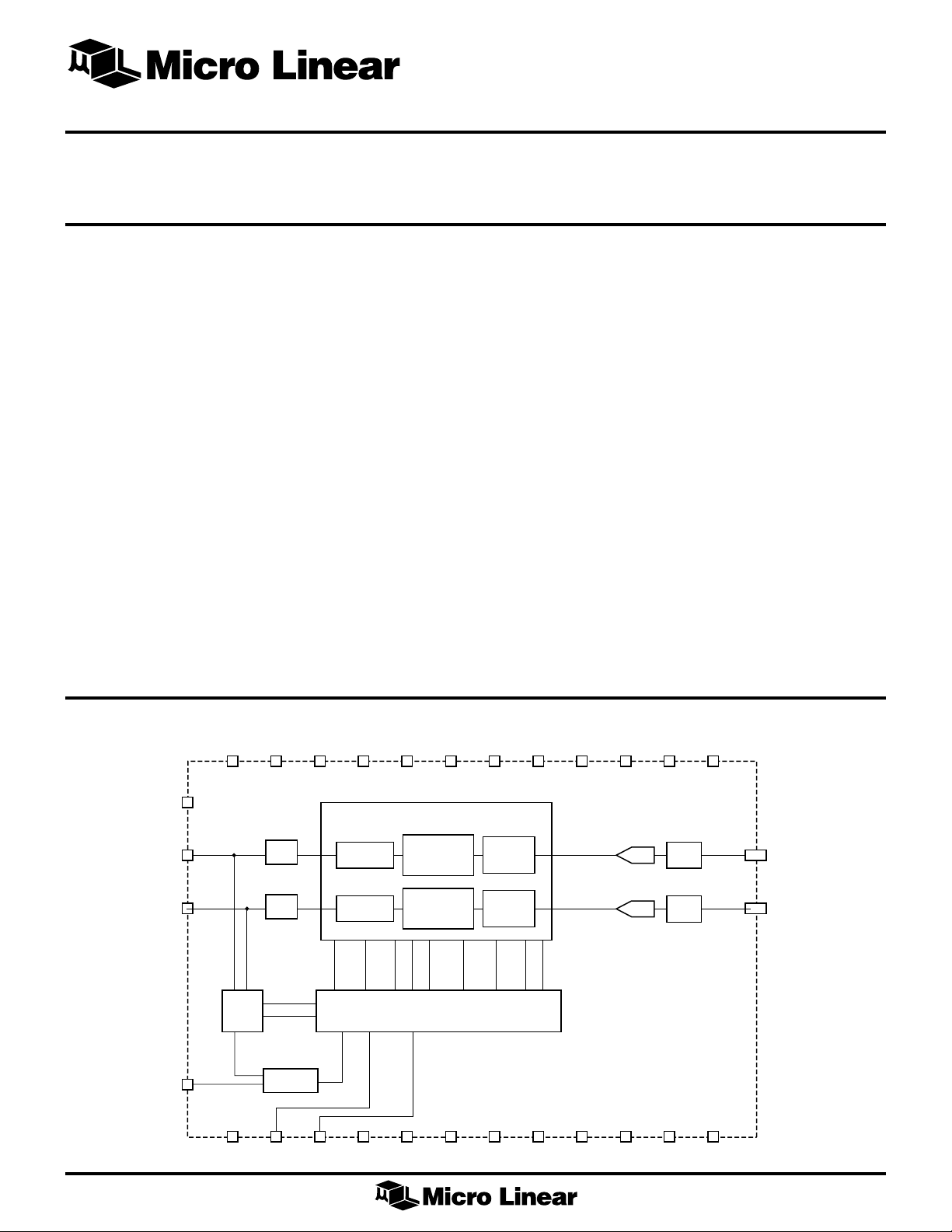
BLOCK DIAGRAM
35
AVCC1
REF1
44
Y/CV1
36
C/CV2
42
CLAMP
SELECT
CLK
14
1
PD
AVCC238AVCC341DVCC17VCCO
CHANNEL A
S/H
CHANNEL B
S/H
CLPA<1:0>
CLPB<1:0>
LEVEL
TIMING
GENERATOR
SCLK19SDAT20REF
GAIN PRESET
GAIN PRESET
STDA <1:0>
CLKDIV
STDB <1:0>
21
IN
APEAK
REF
15 2 33
CLAMP
DGND DVCC
GATE
SGC
SYNC SUPPRESS
GAIN CONTROL
SGC
SYNC SUPPRESS
GAIN CONTROL
BPEAK
22 12 37
OUT
GNA<5:0>
SERIAL BUS
V
CC
GNB<5:0>
AGNDI AGND2
UGC
USER GAIN
CONTROL
UGC
USER GAIN
CONTROL
BOOSTA
32
BOOSTB
CV/S_MODE
40
18
RESET
Y OR CV1
CHANNEL A
C OR CV2
CHANNEL B
43
AGND3
23
OEA
13
GNDO
ADC
ADC
11
OEB
16
DGND
LATCH
Y/CV1
LATCH
C/CV2
39
VINN
A
B
34
NC
OUT
OUT
<7:0>
<7:0>
24:31
3:10
1
Page 2
ML6411
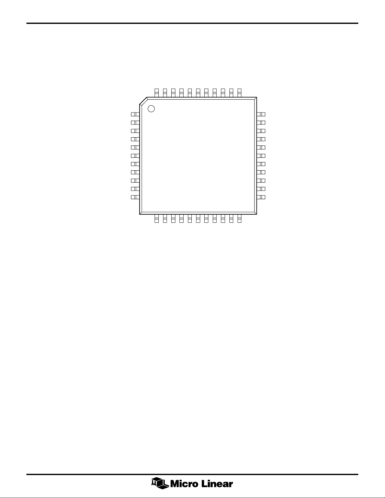
PIN CONFIGURATION
ML6411
44-Pin TQFP (H44-14)
REF1
AGND3
C/CV2
AVCC3
AGND2
VINN
AVCC2
AGND1
Y/CV1
AVCC1
NC
PD
CLAMP GATE
B
OUT
B
OUT
B
OUT
B
OUT
B
OUT
B
OUT
B
OUT
B
OUT
OEB
44 43 42 41 40
1
2
3
0
4
1
5
2
6
3
7
4
8
5
9
6
10
7
11
12 13 14 15 16 17 18 19 20 21 22
CC
CLK
V
GNDO
39 38 37 36 35 34
RESET
DVCC
VCCO
DGND
SCLK
SDAT
IN
REF
OUT
REF
33
32
31
30
29
28
27
26
25
24
23
DGND
DVCC
A
OUT
A
OUT
A
OUT
A
OUT
A
OUT
A
OUT
A
OUT
A
OUT
OEA
7
6
5
4
3
2
1
0
2
Page 3

PIN DESCRIPTION
ML6411
PIN NAME FUNCTION
1 PD When high, power downs the chip.
TTL compatible
2 Clamp Gate Luma clamp gate input. Clamps to
selected level when high. TTL
compatible
3-10 B
<7:0> Either chroma bits 7 (B
OUT
(B
0 LSB) or composite bits 7 (MSB)
OUT
7MSB) to 0
OUT
to 0 (LSB). TTL compatible
11 OEB Output enable for the BOUT channel.
Active low. TTL compatible
12 VCC Reference voltage. Tie to Digital V
CC
13 GNDO Output ground pin
14 CLK Clock input pin. TTL compatible
15 VCCO Output supply pin
16 DGND Digital ground pin
17 DVCC Digital supply pin
PIN NAME FUNCTION
23 OEA Output enable for the AOUT channel.
Active high. TTL compatible
24-31 A
<7:0> Luma bit 7 (A
OUT
0 (A
7 MSB) thru Luma bit
OUT
0 LSB) outputs or Composite
OUT
bit 7 (MSB) thru Composite bit 0 (LSB)
outputs. TTL compatible
32 DVCC Digital supply pin
33 DGND Digital ground pin
34 NC No connection
35 AVCC1 Analog supply pin
36 Y/CV1 Y or CV (primary composite) input pin
37 AGND1 Analog ground pin
38 AVCC2 Analog supply pin
39 VINN Internal common mode bias of the A/D
40 AGND2 Analog ground pin
18 RESET Resets the control registers to nominal
values. Active HIGH. TTL compatible
input
19 SCLK Control Bus Clock. Address latched on
rising edge, data on falling edge
20 SDA T Control data
21 REF
22 REF
IN
OUT
Internal reference tied to REF
Internal reference tied to REF
OUT
IN
41 AVCC3 Analog supply pin
42 C/CV2 C (modulated chroma) or CV (2
nd
composite for dual channel mode)
input pin
43 AGND3 Analog ground pin
44 REF1 Internal reference. Tie this pin thru
0.1uF capacitor to analog ground for
proper operation
3
Page 4

ML6411
ABSOLUTE MAXIMUM RATINGS
Absolute maximum ratings are those values beyond which
the device could be permanently damaged. Absolute
OPERATING CONDITIONS
Temperature Range........................................ 0°C to 70°C
Supply Range (AVCC, DVCC, VCCO) ...........4.5V to 5.5V
maximum ratings are stress ratings only and functional
device operation is not implied.
DC Supply Voltage (AVCC, DVCC, VCCO) .... -0.3V to 7V
Analog & Digital Inputs/Outputs ........ -0.3 to AVCC+0.3V
Input Current Per Pin .............................. -25mA to 25mA
Storage Temperature Range...................... –65°C to 150°C
Junction T emperature............................................. 125°C
ELECTRICAL CHARACTERISTICS
Unless otherwise specified, AVCC, DVCC, VCCO = 4.5V to 5.5V , TA = Operating Temperature Range (Note 1)
SYMBOL PARAMETER CONDITIONS MIN TYP MAX UNITS
POWER CONSUMPTION
P
diss
SUPPLY
AVCC Analog supply voltage 4.5 5.5 V
Max power dissipation Cload = 0pF 425 600 mW
DVCC Digital supply voltage 4.5 5.5 V
VCCO Output supply voltage 4.5 5.5 V
IDD Digital supply current FCLK = 30MHz 17 30 mA
I
I
shut
INPUT SIGNALS (CLK, CLAMP GATE, OEA, OEB)
V
V
I
C
IN1
INPUT SIGNALS (Y / CV1, C / CV2)
V
C
Input Capacitance 3pF
IN2
I
charge
I
disch
Output supply current FCLK=30MHz, VIN=NTSC, 7 mA
O
Shutdown current 5mA
Input Low Voltage 0 0.8 V
IL
Input High Voltage 2.4 DV
IH
High level Input Current DVCC - 0.1V -5 5 µA
IL
Input Capacitance 3pF
Input Voltage Peak-to-peak for 2V 1.0 2.0 3.0 V
IN
Clamp Charge Current Clamp Gate = High, 700 µA
Clamp Discharge Current Clamp Gate = High, –700 µA
40IRE modulated rate, Cload=0pF
CC
Peak-to-peak for 1V 0.5 1.0 1.5 V
Digital Output < Clamp level
Digital Output > Clamp level
V
A TO D CONVERTER OUTPUTS (A
Low level output voltage Io = 2mA 0 0.6 V
High level output voltage 2.4 VCCO
Leakage current Tri-state mode -20 20 µA
4
OUT
<7:0>, B
OUT
<7:0>)
Page 5
ML6411
ELECTRICAL CHARACTERISTICS (Continued)
SYMBOL PARAMETER CONDITIONS MIN TYP MAX UNITS
SWITCHING CHARACTERISTICS
FCLK Clock input max frequency 30 MHz
T
cph
T
Clock input min high time See Figure 2 15 ns
Clock input min low time See Figure 2 15 ns
cpl
Clamp Gate Width VIN magnitude 2V max 1.5 µs
Clamp Gate Width VIN magnitude > 2V 3.5 µs
ANALOG SIGNAL PROCESSING
Y/C Gain Match CGAIN1 = CGAIN2 = 0 1.01 V/V
Chroma Crosstalk Y
Differential Gain V
Differential Phase V
Signal to Noise Ratio V
Distortion VIN = 2V, 10MHz, FCLK = 20MHz 0.3 %
SFDR VIN = 2V, 10MHz, FCLK = 20MHz 54 dB
TRANSFER FUNCTION
= 5MHz and CIN = at DC; –60 dB
IN
or YIN = at DC and CIN = 5MHz
= NTSC 40 IRE modulated ramp 2 %
IN
FCLK = 27 MHz
= NTSC 40 IRE modulated ramp 1 degree
IN
FCLK = 27 MHz
= 2V, 10MHz sinewave, 48 dB
IN
FCLK = 20MHz
VIN = 2V, 10MHz sinewave, 45 dB
FCLK = 30MHz
DC integral linearity @ 27MHz ±0.8 LSB
DC differential linearity @ 27MHz ±0.5 LSB
GAIN CONTROL
G
Gain accuracy of UGC for a given gain level Input = 1V
RES
P-P or 2VP-P
Absolute gain error 5%
Gain accuracy for standard preset gain, 1 %
G
PRESET
OUTPUT TIMING
t
t
ho
t
do
t
t
od
Note 1: Limits are guaranteed by 100% testing, sampling, or correlation with worst-case test conditions.
Note 2: Volt Peak-to-Peak = V
Sampling delay See Figure 2 8 ns
ds
Output hold time See Figure 2 10 ns
Output delay time See Figure 2 12 ns
Output enable time See Figure 2 5 ns
oe
Output disable time See Figure 2 5 ns
P-P
(See Note 2) -30mV 30mV %
5
Page 6
ML6411
SERIAL BUS
Unless otherwise specified, AVCC, DVCC, VCCO = 4.5V to 5.5V , TA = Operating Temperature Range (Note 1)
SYMBOL PARAMETER CONDITIONS MIN TYP MAX UNITS
INPUT (SDAT)
V
V
I
I
Z
C
Low Level Input Voltage 0 0.8 V
IL
High Level Input Voltage VCC – 0.8 V
IH
Low Level Input Current VIN = 0V 1.0 mA
IL
High Level Input Current VIN = DV
IH
Input Impedance f
IN
Input Capacitance 2pF
IN
SYSTEM TIMING (SCLK)
f
CLOCKSCLK
V
HYS
t
SPIKE
t
WAIT
t
HD/START
t
SU/START
t
LOW
t
HI
t
HD/DATA
t
SU/DATA
Frequency 100 kHz
Input Hysteresis 0.2 V
Spike Suppression Max Length for Zero Response 50 ns
Wait Time From STOP to START
On S
DATA
Hold Time for START On S
Setup Time for START On S
Min LOW Time On S
Min HIGH Time On S
Hold Time On S
Setup Time On Fast mode 100 ns
DATA
CLK
CLK
DATA
DATA
CC
CC
= 100kHz 1 MW
CLK
1.0 mA
1.3 µs
0.6 µs
0.6 µs
1.3 µs
0.6 µs
5.0 µs
Slow mode 250 ns
V
t
LH
t
HL
t
SU/STOP
Note 1: Limits are guaranteed by 100% testing, sampling, or correlation with worst case test conditions.
Note 2: All specifications include reconstruction filter and line driver.
Note 3: Normalized to burst.
Rise Time for S
Fall Time for S
CLK
CLK
& S
& S
DATA
DATA
Setup Time for STOP On S
DATA
30 300 ns
30 300 ns
0.6 µs
6
Page 7

FUNCTIONAL DESCRIPTION
ML6411
GENERAL
The Univ ersal Video Digitizer is a single-chip Video A/D
converter with an analog front end which is intended for
analog to digital conversion of 2V peak-to-peak (V
1V
signals at rates up to 30 MSPS through a high
P-P
P-P
) or
performance A/D with ±½ DNL performance. It forms a
complete solution for data conversion of dual CV and Y/C
signals including gain settings and clamp settings by
incorporating clamps, user selectable gain controls (UGC
and SGC), bias and clock generation.
The ML6411 consist of two video clamps, two sample and
hold amplifiers, two three-stage pipeline A/D converters,
digital error correction circuitry, selectable clamps,
programmable gain control, bias voltage generation and
clock generation. The operating power dissipation is
425mW typical.
INPUT FOR VARIOUS VIDEO MODES
The ML6411 can digitize various analog video inputs:
S-Video (Y/C), or composite video (CV). Again, for each
video channel, the gain and clamps can be selected.
A description of each of these modes is described
below. The Table 1 below provides a summary of the
various modes.
Dual Channel Composite Video (CV1 and CV2) Mode
Control (UGC). Standard gain selection can also be
chosen using the preset gain modes for 2V
For 1V
signals, the preset gain selection mode is not
P-P
signals only.
P-P
available; however the UGC functions can be used to
select gain values. The preset gain modes are for typical
NTSC or PAL S-Video and are selectable via serial bus
through the STDA<1:0> and STDB<1:0> (Register B , Bits
B4, B3, B2, and B1) bits. When using the preset gain
mode, the output signals are enhanced by amplifying the
input signal by the value of G
(see Table 2). In
PRESET
addition, the clamp levels can be selected for either
channel for 16, 24, 64, and 128 binary levels (depending
on the channel 24 not av ailable for C-c hannel) via the
serial bus through the CLPA<1:0> and CLPB<1:0> bits (see
Table 3).
Input Voltage Selection
The ML6411 can support 1V
and 2V
P-P
input video.
P-P
Selection for the voltage input is programmed via control
register on the APEAK and BPEAK bits, A channel and B
channel, respectively (see Table 7).
GAIN SELECTION CONTROL (UGC AND SGC)
There are two separ ate control mechanisms that can be
used to scale gain settings for the incoming video format:
User Gain Control (UGC) and Sync-suppressed Gain
Control (SGC).
The composite input channels are provided through the Y/
CV1 (A channel) and C/CV2 (B channel) pins. T o activate
this mode, the CV/S_Mode Bit (Register D, Bit D3) must set
HIGH (D3=1). This mode is selectable via serial bus. In
this mode, the two S&H circuits for each channel can be
clocked up to 30MHz. Each CV channel can be then
scaled for a desired gain setting using the User Gain
Control (UGC). Standard gain selection can also be
chosen using the preset gain modes for 2V
For 1V
signals, the preset gain selection mode is not
P-P
signals only.
P-P
available; however the UGC functions can be used to
select gain values. The preset gain modes are for typical
NTSC or PAL composite video and are selectable via serial
bus through the STDA<1:0> and STDB<1:0> (Register B ,
Bits B4, B3, B2, and B1) bits. When using the preset gain
mode, the output signals are enhanced by amplifying the
input signal by the value of G
(see Table 2). In
PRESET
addition, the clamp levels can be selected for either
channel for 16, 24, 64, and 128 binary levels (depending
on the channel) via the serial bus through the CLPA<1:0>
and CLPB<1:0> bits (see Table 3).
S-Video (Y / C) Mode
The input channels are pro vided through the Y/CV1 (A
channel) and C/CV2 (B channel) pins. To activate this
mode, the CV/S_Mode Bit (Register D, Bit D3) must be set
LOW (D3=0). This mode is selectable via serial bus. In this
mode, the two S&H circuits for each channel can be
clocked up to 30MHz. Each channel (Y and C) can be
then scaled for a desired gain setting using the User Gain
User Gain Control (UGC)
The user gain control function is achiev ed through a
variation of the full scale range of the A/D con v erters. This
will provide the user with approximately +/-3dB gain
variation as needed. Y reference and C reference are
supplied by two independent DACs. The user can adjust
the gain of each ADC independently providing the 6-Bit
code for the gain control through serial interface for each
A/D. Each step change can increment or decrement the
gain by 3% and allows for up to 64 different gain setting
levels per channel. The UGC can be used for both 1V and
2V
inputs. When using the UGC mode, the output
P-P
signals are enhanced by amplifying the input signal by the
value of G
. Table 4 provides a summary of the possible
UGC
incremental ranges. The gain accuracy of the UGC for
each of the 64 levels is +/-1.5%. The UGC gain settings
are selected via serial bus by programming Registers C, D,
and E on the GNA<5:0> bits for the A-channel and
GNB<5:0> bits for the B-channel.
Unity gain is set at default for GNA<5:0> = 100,000 and
GNB<5:0> = 100,000. For v alues of GNA<5:0> and
GNB<5:0> from 100,000 to 111,111, the gain increases
monotonically from 0dB (unity gain) to almost 3dB
(actually 1.48x), while from 100,000 to 000,000 the gain
decreases monotonically from 0dB (unity gain) to –3dB
(0.5x). Note that Table 4 provides only approximation of
gain values: actual gain values can vary from device to
device.
7
Page 8

ML6411
FUNCTIONAL DESCRIPTION (Continued)
Sync-suppress Gain Control (SGC)
This control function is used for video where the sync
signal is suppressed (i.e., chroma signal). In which case,
the SGC can be activated to provide a 25% gain boost to
each channel (Y and C). The SGC is activated via serial bus
(Register D, Bits D1 and D2), also called the BOOSTA and
BOOSTB programming bits. In the SGC mode, the output
signals are enhanced by amplifying the input signal by the
value of G
(see Table 5).
SGC
Using The Gain Control Blocks Together
The UGC combined provides digital gain control data to a
variable gain control circuit while the SGC is directly in
the A/D processing path. Hence the UGC sets variable
gain control of the A/D.
When the UGC and the SGC are enabled. In this mode,
the output gain is the combination of the different gain
setting mechanisms:
For 1V
signals,
P-P
Equation 1: Output Gain = [<Input Signal> x
G
UGC
For 2V
x G
P-P
] + Clamp Level
SGC
signals,
Equation 2: Output Gain = [<Input Signal> x
G
x G
UGC
Note that separate G
SGC
UGC
x G
PRESET
, G
] + Clamp Level
, and G
SGC
PRESET
values are
available for both c hannels A and B. There are up to 640
combinations of gain settings possible.
WARNING
Note that it is possible to exceed the output voltage ranges
for standard video using the combination of the gain
setting mechanisms on the input signal. The user should
take precaution in understanding the gain limits necessary
and make the proper selection for each of the gain
mechanism.
A/D CONVERTER
cycle later, after the subtraction/amplification of the first
stage has settled. The third stage A/D performs the
conversion after another one-half cycle dela y, when the
second stage has settled. Error correction is then
performed and, one clock cycle later, data is transferred to
the output latch. This creates a 3 clock latency.
INPUT SAMPLE AND HOLD
The input sample and hold consist of a bottom plate
sampling capacitor feedback amplifier. The input
capacitance is 0.4pF, plus transmission gate. The input to
the sample and hold is driven differentially. The sample
and hold samples the input signal during the positive half
cycle of the input clock, and holds the last v alue of the
input during the negative half cycle of the input cloc k. The
settling time of the amplifier is less than 10nS.
INPUT COUPLING AND DC CLAMP PROGRAM
SELECTION
All inputs are A C coupled into the positi v e sampling
capacitor of the sample and hold. Each input capacitor
becomes the integrating component for the DC restore
clamps. The direction of clamp current depends on the
data at the A/D output during the clamp gating pulse. For
the color channel (i.e. C in Y/C mode) the clamp level is
128. If the code is above this number during the gate
pulse, the current source will sink current from the input
capacitor in order to drive the input voltage lo wer.
Otherwise, the current source will source current to raise
the input voltage. Clamp currents are shown in Table 6.
The clamp values of 16, 24, 64, 128 can be select via
register program (Register A and B) through the serial bus.
Note that there is no Level 24 in the B channel. The
CLPA<1:0> controls the clamp settings for the
A-channel, while the CLPB<1:0> controls the clamp
settings for the B-channel. For example, clamp values can
be selected independently for the chroma channel in Y/C
mode (CLPB<1:0>). Once the clamp settings are selected,
the clamps are active when the ClampGate is asserted
HIGH. The ClampGate signal is an external signal provided
by a genlock/sync cloc k device that is genloc ked to the
horizontal sync of the video input. T he ML6431 can be used
to generate the ClampGate signal (see Application Section).
The A/D conversion is performed via a three stage pipeline
architecture. The first two stages quantize their input signal
to the three bits, then subtract the result from the input and
amplify by a factor of four. This creates a residue signal
which spans the full scale range of the following converter.
The subtraction and amplification is performed via a
bottom plate sampling capacitor feedback amplifier,
similar to the input sample and hold. The third stage
quantizes the signal to four bits. One bit from each of the
last two stages is used for error correction.
The first stage A/D performs the conversion at the end of
the sample and holds period, approximately one-half
8
SERIAL PROGRAM
The ML6411 can be register programmed through the
serial bus. Clamping and gain setting can be selected for
various video formats. This serial bus is a standard threepin interface with data, clock, and ground. See Timing
Control information. Table 7 provides a description the
Register information. Please see section “Input Coupling
and DC Clamp Program Selection” and “Gain Select
Control”.
Page 9

FUNCTIONAL DESCRIPTION (Continued)
ML6411
RESET DEFAULT MODE
■ UGC is set to unity gain (G
UGCA
either Y or C channels (see Table 4 and GNA and GNB
The ML6411 provides a RESET pin that programs the
bits)
Control Registers as described in Table 8. The RESET pin is
active HIGH. Basically, the ML6411 on RESET defaults to:
■ S-Video mode. Ideally, for PAL S-Video since Preset
■ Input pin are set for 2V
inputs on both Y and C
P-P
Mode (STDA and STDB bits) is set to unity gain boost
(G
■ Y is clamped to 16. C is clamped to 128 (see Table 3)
= 1) for both Y and C (see Table 2)
PRESET
and CLPA and CLPB bits)
MODE REGISTER/BIT VALUES CHANNEL SIGNAL INPUT OUPUT OPTIONS
Dual CV Register D, A CV1 Y/CV1 pin A
OUT
<7:0>
Gain Control Selection
Bit D3= CV/S_Mode =1 (UGC, SGC) and Clamp
Selection.
1V
P-P or 2VP-P
Serial Bus Programable.
B CV2 C/CV2 pin B
S-Video Register D, A Y Y/CV1 pin A
OUT
OUT
<7:0>
<7:0>
Gain Control Selection
Bit D3= CV/S_Mode =0 (UGC, SGC) and Clamp
Selection.
1V
P-P or 2VP-P
Serial Bus Programable.
OUT
<7:0>
Note: Volt Peak-to-Peak = V
B C C/CV2 pin B
P-P
= 1 and G
inputs.
inputs.
UGCB
= 1) to
Table 1. Various Video Modes Using the ML6411 and Key Features
9
Page 10

ML6411
DUAL COMPOSITE VIDEO MODE
TYPICAL INPUTS GAIN SELECTION GAIN FACTOR OF
OF AMPLIFIERS AMPLIFIERS (nominal)
Channel A Channel B Channel A Channel B Channel A Channel B
STANDARD CV1 Input (mV) CV2 Input (mV) STDA<1:0> STDB<1:0> G
Composite Video NTSC 1320 1320 01 01 1.061 1.061
Composite Video PAL 1400 1400 00 00 1 1
Preset Mode 1 1320 1320 01 11 1.061 0.7495
Preset Mode 2 1428 1428 11 00 1.02 1
Preset Mode 3 1400 1400 00 11 1 0.7495
Preset Mode 4 1294 1294 10 10 1.082 1.082
PRESET A
S-VIDEO MODE
TYPICAL INPUTS GAIN SELECTION GAIN FACTOR OF
OF AMPLIFIERS AMPLIFIERS (nominal)
Channel A Channel B Channel A Channel B Channel A Channel B
STANDARD Y Input (mV) C Input (mV) STDA<1:0> STDB<1:0> G
S-Video NTSC 1320 1320 01 01 1.061 1.061
S- Video PAL 1400 1400 00 00 1 1
Preset Mode 1 1320 1320 01 11 1.061 0.7495
Preset Mode 2 1428 1428 11 00 1.02 1
Preset Mode 3 1400 1400 00 11 1 0.7495
Preset Mode 4 1294 1294 10 10 1.082 1.082
PRESET A
G
PRESETB
G
PRESETB
Table 2. Video Standard Preset Gain Selection Modes
10
Page 11

ML6411
DUAL COMPOSITE MODE
CLAMP LEVEL CLPA1 BIT CLPA0 BIT NOTES
Channel A (CV1) 16 0 0 Typical CV Clamp. Defaults to this value on RESET
24 1 0
64 0 1
128 1 1
CLAMP LEVEL CLPB1 BIT CLPB0 BIT NOTES
Channel B (CV2) 16 1 0 Typical CV clamp.
64 1 1
128 0 X Defaults to this value on RESET
S-VIDEO MODE
CLAMP LEVEL CLPA1 BIT CLPA0 BIT NOTES
Channel A (Y) 16 0 0 T ypical Y clamp. Defaults to this value on RESET
24 1 0
64 0 1
128 1 1
CLAMP LEVEL CLPB1 BIT CLPB0 BIT NOTES
Channel B (C) 16 1 0
64 1 1
128 0 X T ypical C clamp. Defaults to this value on RESET
Note: X = Don't Care
Table 3. Programmable Clamp Level Selection
11
Page 12

ML6411
A-CHANNEL
GNA5 GNA4 GNA3 GNA2 GNA1 GNA0 GAIN
FACTOR
G
UGCA
(NOMINAL)
1 1 0 0 0 0 0 0.50
2 1 0 0 0 0 1 0.52
3 1 0 0 0 1 0 0.53
4 1 0 0 0 1 1 0.55
5 1 0 0 1 0 0 0.56
6 1 0 0 1 0 1 0.58
7 1 0 0 1 1 0 0.59
8 1 0 0 1 1 1 0.61
9 1 0 1 0 0 0 0.63
10 1 0 1 0 0 1 0.64
11 1 0 1 0 1 0 0.66
12 1 0 1 0 1 1 0.67
13 1 0 1 1 0 0 0.69
14 1 0 1 1 0 1 0.70
15 1 0 1 1 1 0 0.72
16 1 0 1 1 1 1 0.73
17 1 1 0 0 0 0 0.75
18 1 1 0 0 0 1 0.77
19 1 1 0 0 1 0 0.78
20 1 1 0 0 1 1 0.80
21 1 1 0 1 0 0 0.81
22 1 1 0 1 0 1 0.83
23 1 1 0 1 1 0 0.84
24 1 1 0 1 1 1 0.86
25 1 1 1 0 0 0 0.88
26 1 1 1 0 0 1 0.89
27 1 1 1 0 1 0 0.91
28 1 1 1 0 1 1 0.92
29 1 1 1 1 0 0 0.94
30 1 1 1 1 0 1 0.95
31 1 1 1 1 1 0 0.97
32 1 1 1 1 1 1 0.98
33 0 0 0 0 0 0 1.00
34 0 0 0 0 0 1 1.02
35 0 0 0 0 1 0 1.03
36 0 0 0 0 1 1 1.05
37 0 0 0 1 0 0 1.06
38 0 0 0 1 0 1 1.08
39 0 0 0 1 1 0 1.09
40 0 0 0 1 1 1 1.11
41 0 0 1 0 0 0 1.13
42 0 0 1 0 0 1 1.14
43 0 0 1 0 1 0 1.16
44 0 0 1 0 1 1 1.17
45 0 0 1 1 0 0 1.19
46 0 0 1 1 0 1 1.20
47 0 0 1 1 1 0 1.22
48 0 0 1 1 1 1 1.23
49 0 1 0 0 0 0 1.25
50 0 1 0 0 0 1 1.27
51 0 1 0 0 1 0 1.28
52 0 1 0 0 1 1 1.30
53 0 1 0 1 0 0 1.31
54 0 1 0 1 0 1 1.33
55 0 1 0 1 1 0 1.34
56 0 1 0 1 1 1 1.36
57 0 1 1 0 0 0 1.38
58 0 1 1 0 0 1 1.39
59 0 1 1 0 1 0 1.41
60 0 1 1 0 1 1 1.42
61 0 1 1 1 0 0 1.44
62 0 1 1 1 0 1 1.45
63 0 1 1 1 1 0 1.47
64 0 1 1 1 1 1 1.48
Table 4. Gain Approximations for User Gain Control (UGC) Block
B-CHANNEL
GNB5 GNB4 GNB3 GNB2 GNB1 GNB0 GAIN
FACTOR
G
UGCB
(NOMINAL)
1 1 0 0 0 0 0 0.50
2 1 0 0 0 0 1 0.52
3 1 0 0 0 1 0 0.53
4 1 0 0 0 1 1 0.55
5 1 0 0 1 0 0 0.56
6 1 0 0 1 0 1 0.58
7 1 0 0 1 1 0 0.59
8 1 0 0 1 1 1 0.61
9 1 0 1 0 0 0 0.63
10 1 0 1 0 0 1 0.64
11 1 0 1 0 1 0 0.66
12 1 0 1 0 1 1 0.67
13 1 0 1 1 0 0 0.69
14 1 0 1 1 0 1 0.70
15 1 0 1 1 1 0 0.72
16 1 0 1 1 1 1 0.73
17 1 1 0 0 0 0 0.75
18 1 1 0 0 0 1 0.77
19 1 1 0 0 1 0 0.78
20 1 1 0 0 1 1 0.80
21 1 1 0 1 0 0 0.81
22 1 1 0 1 0 1 0.83
23 1 1 0 1 1 0 0.84
24 1 1 0 1 1 1 0.86
25 1 1 1 0 0 0 0.88
26 1 1 1 0 0 1 0.89
27 1 1 1 0 1 0 0.91
28 1 1 1 0 1 1 0.92
29 1 1 1 1 0 0 0.94
30 1 1 1 1 0 1 0.95
31 1 1 1 1 1 0 0.97
32 1 1 1 1 1 1 0.98
33 0 0 0 0 0 0 1.00
34 0 0 0 0 0 1 1.02
35 0 0 0 0 1 0 1.03
36 0 0 0 0 1 1 1.05
37 0 0 0 1 0 0 1.06
38 0 0 0 1 0 1 1.08
39 0 0 0 1 1 0 1.09
40 0 0 0 1 1 1 1.11
41 0 0 1 0 0 0 1.13
42 0 0 1 0 0 1 1.14
43 0 0 1 0 1 0 1.16
44 0 0 1 0 1 1 1.17
45 0 0 1 1 0 0 1.19
46 0 0 1 1 0 1 1.20
47 0 0 1 1 1 0 1.22
48 0 0 1 1 1 1 1.23
49 0 1 0 0 0 0 1.25
50 0 1 0 0 0 1 1.27
51 0 1 0 0 1 0 1.28
52 0 1 0 0 1 1 1.30
53 0 1 0 1 0 0 1.31
54 0 1 0 1 0 1 1.33
55 0 1 0 1 1 0 1.34
56 0 1 0 1 1 1 1.36
57 0 1 1 0 0 0 1.38
58 0 1 1 0 0 1 1.39
59 0 1 1 0 1 0 1.41
60 0 1 1 0 1 1 1.42
61 0 1 1 1 0 0 1.44
62 0 1 1 1 0 1 1.45
63 0 1 1 1 1 0 1.47
64 0 1 1 1 1 1 1.48
12
Page 13

ML6411
CHANNEL REGISTER/BIT VALUES GAIN FACTOR
A REGISTER D, BIT D1 = "BOOSTA" = 0 G
REGISTER D, BIT D1 = "BOOSTA" = 1 G
B REGISTER D, BIT D2 = "BOOSTB" = 0 G
REGISTER D, BIT D2 = "BOOSTB" = 1 G
Table 5. SGC Gain Mode
CLAMP GATE SIGNAL CLAMP LEVEL OUTPUT CLAMP CURRENT
0X X0
1 00 OUT < 16 700µA
00 OUT > 16 –700µA
01 OUT < 64 700µA
01 OUT > 64 –700µA
10 OUT < 24 700µA
10 OUT > 24 –700µA
11 OUT < 128 700µA
11 OUT > 128 –700µA
SGCA
SGCA
SGCB
SGCB
= 1
= 1.25
= 1
= 1.25
Table 6: Clamp Current for Various Clamp Levels
13
Page 14

ML6411
REGISTER INFORMATION AND ORGANIZATION
REGISTER ADDRESS DATA BIT NAME DESCRIPTION BIT CODE RANGE
A 000 A0 CLPA0 Sets Clamp Lev el for the A Channel See Table 3
A1 CLPA1 Sets Clamp Level for the A Channel See Table 3
A2 Reserved Reserved Don't Care
A3 Reserved Reserved Don't Care
A4 CLPB0 Sets Clamp Level for the B Channel See Table 3
B 001 B0 CLPB1 Sets Clamp Level for the B Channel See Table 3
B1 STDB0 Selects Standard Preset Gain Level for B Channel See Table 2
B2 STDB1 Selects Standard Preset Gain Level for B Channel See Table 2
B3 STDA0 Selects Standard Preset Gain Level for A Channel See Table 2
B4 STDA1 Selects Standard Preset Gain Level for A Channel See Table 2
C 010 C0 GNA0 Sets User Defined Gain Level for A Channel See Table 4
C1 GNA1 Sets User Defined Gain Level for A Channel See Table 4
C2 GNA2 Sets User Defined Gain Level for A Channel See Table 4
C3 GNA3 Sets User Defined Gain Level for A Channel See Table 4
C4 GNA4 Sets User Defined Gain Level for A Channel See Table 4
D 011 D0 GNA5 Sets User Defined Gain Level for A Channel See Table 4
D1 BOOSTA Provides 25% Extra Gain on A Channel 0 = 1 x Gain;
D2 BOOSTB Provides 25% Extra Gain on B Channel 0 = 1 x Gain;
D3 CV/S_Mode Select Dual Composite Mode or S-Video Mode 0 = S-Video Mode;
D4 GNB0 Selects User Defined Gain Level for B Channel See Table 4
E 100 E0 GNB1 Sets User Defined Gain Level for B Channel See Table 4
E1 GNB2 Sets User Defined Gain Level for B Channel See Table 4
E2 GNB3 Sets User Defined Gain Level for B Channel See Table 4
E3 GNB4 Sets User Defined Gain Level for B Channel See Table 4
E4 GNB5 Sets User Defined Gain Level for B Channel See Table 4
F 101 F0 Reserved Set to 0 for Proper Operation F0 = 0
F1 APEAK Sets A Channel for 1V
or 2V
inputs 0 = 2V
P-P
F2 BPEAK Sets A Channel for 1V
or 2V
inputs 0 = 2V
P-P
P-P
P-P
F3 CLKDIV Sets Internal Clock Frequency to Divide-by-2 1 = 1V
F4 Reserved Recommend 0 for RESET and 1 for Normal Operation 0 or 1 is Acceptable
Note: Volt Peak-to-Peak = V
P-P
1 = 1.25 x Gain;
See T able 5
1 = 1.25 x Gain;
See T able 5
1 = Dual Composite
Mode
1 = 1V
P-P
P-P
1 = 1V
P-P
P-P
P-P
0 = 2V
P-P
14
Table 7: Control Register Summary
Page 15

ML6411
REGISTER INFORMATION AND ORGANIZATION
REGISTER ADDRESS DATA BIT NAME DESCRIPTION DEFAULT SETTING
A 000 A0 CLPA0 Sets Clamp Level for the A Channel to 16 0
A1 CLPA1 0
A2 Reserved Reserved X
A3 Reserved Reserved X
A4 CLPB0 Sets Clamp Level for the B Channel to 128 X
B 001 B0 CLPB1 Sets Clamp Level for the B Channel to 128 0
B1 STDB0 Selects Standard Preset Gain Level for B Channel (See Table 2) 0
B2 STDB1 Selects Standard Preset Gain Level for B Channel (See Table 2) 0
B3 STDA0 Selects Standard Preset Gain Level for A Channel (See Table 2) 0
B4 STDA1 Selects Standard Preset Gain Level for A Channel (See Table 2) 0
C 010 C0 GNA0 Sets User Defined Gain Level for A Channel (See Table 4) 0
C1 GNA1 Sets User Defined Gain Level for A Channel (See Table 4) 0
C2 GNA2 Sets User Defined Gain Level for A Channel (See Table 4) 0
C3 GNA3 Sets User Defined Gain Level for A Channel (See Table 4) 0
C4 GNA4 Sets User Defined Gain Level for A Channel (See Table 4) 0
D 011 D0 GNA5 Sets User Defined Gain Level for A Channel (See Table 4) 1
D1 BOOSTA Provides 25% Extra Gain on A Channel 0 = 1 x Gain
D2 BOOSTB Provides 25% Extra Gain on B Channel (See Table C) 0 = 1 x Gain
D3 CV/S_Mode Select Dual Composite Mode or S-Video Mode 0 = S-Video Mode
D4 GNB0 Selects User Defined Gain Level for B Channel (See Table 4) 0
E 100 E0 GNB1 Sets User Defined Gain Level for B Channel (See Table 4) 0
E1 GNB2 Sets User Defined Gain Level for B Channel (See Table 4) 0
E2 GNB3 Sets User Defined Gain Level for B Channel (See Table 4) 0
E3 GNB4 Sets User Defined Gain Level for B Channel (See Table 4) 0
E4 GNB5 Sets User Defined Gain Level for B Channel (See Table 4) 1
F 101 F0 Reserved Set to 0 for Proper Operation 0
F1 APEAK Sets A Channel for 1V
F2 BPEAK Sets A Channel for 1V
F3 CLKDIV Sets Internal Clock Frequency to Divide-by-2 0 = CLK
or 2V
or 2V
P-P
P-P
inputs
inputs
P-P
P-P
0 = 2V
0 = 2V
P-P
P-P
Note: X = Don't Care
Note: Volt Peak-to-Peak = V
F4 Reserved Recommend 0 for RESET and 1 for Normal Operation 0
P-P
Table 8: RESET Control Valures of Control Register
15
Page 16

ML6411
REGISTER INFORMATION AND ORGANIZATION
REGISTER A
ADDRESS RA <2:0> = <000>
MSB
A4 A3 A2 A1 A0 X
DEVICE INFORMATION
DEVICE ADDRESS: B5
REGISTOR ADDRESS BITS:
RA <2:0>
DATA BITS: <4:0>X
CONTROL REGISTERS:
REGISTER A
ADDRESS RA <2:0> = <000>
DATABITS A <4:0> X
REGISTER B
ADDRESS RA <2:0> = <001>
REGISTER C
ADDRESS RA <2:0> = <010>
REGISTER D
ADDRESS RA <2:0> = <011>
REGISTER E
ADDRESS RA <2:0> = <100>
MSB
B4 B3 B2 B1 B0 X
MSB
C4 C3 C2 C1 C0 X
MSB
D4 D3 D2 D1 D0 X
MSB
E4 E3 E2 E1 E0 X
REGISTER B
ADDRESS RA <2:0> = <001>
DATABITS B <4:0> X
REGISTER C
ADDRESS RA <2:0> = <010>
DATABITS C <4:0> X
REGISTER D
ADDRESS RA <2:0> = <011>
DATABITS D <4:0> X
REGISTER E
ADDRESS RA <2:0> = <100>
DATABITS E <4:0> X
16
REGISTER F
ADDRESS RA <2:0> = <101>
MSB
F4 F3 F2 F1 F0 X
X = DUMMY BIT FOR ACKNOWLEDGE
Figure 1. Register Organization and Information
REGISTER F
ADDRESS RA <2:0> = <101>
DATABITS F <4:0> X
Page 17

TIMING CONTROL
ML6411
The ML6411 operates in master mode w here all internal
timing is derived from the clock input at the CLK pin.
Figure 2 provides timing diagrams for both the Dual
Composite and Y/C modes. Note that the REF OUT pin
provides the internal timing to the REF IN pin. These pins
are shorted together for normal operation.
Serial Bus Timing. Figure 3 provides timing of serial bus
mode. Figure 4 provides a detailed timing for device,
register , and data insertion to the control registers. As
SAMPLE
N
SAMPLE
N +1
shown in Figure 1, there are six independent 5-bit registers
in the Control Block. To load a register, the 3-bit address is
loaded in first followed by the 5-bit data values and a
dummy bit. This is a total of 9-bits to load a register with
the last bit being a dummy bit. Note that all of the registers
can be loaded in succession before the STOP condition is
enabled.
The CLKDIV function provides an internal divide-by-2
clock. This function is enable via control register.
SAMPLE
N +2
SAMPLE
N +3
SAMPLE
N +4
V
CLK
S/H CHANNEL A
S/H CHANNEL A
OEC
OEY
Y<7:0>
C<7:0>
CV1<7:0>
CV2<7:0>
t
IN
t
ds
SAMPLE
SAMPLE HOLD SAMPLE HOLD SAMPLE HOLD SAMPLE HOLD SAMPLE HOLD SAMPLE HOLD SAMPLE HOLD
HOLD SAMPLE HOLD SAMPLE HOLD SAMPLE HOLD SAMPLE HOLD SAMPLE HOLD SAMPLE HOLD
Y
n -3
C
n -3
t
od
Y
n -2
C
n -2
t
oe
Y
n -1
C
n -1
t
ho
t
do
cph
t
cpl
Y
n
C
n
Y
C
n +1
n +1
Y
C
n +2
n +2
Figure 2. Y/C and Dual CV Mode
17
Page 18

ML6411
S
DATA
START
t
SET/START
S
CLK
START: A Falling Edge on the S
STOP: A Rising Edge on the S
START
S
S
DATA
CLK
MSB
0
1 2 7 8 9 10 11 12 13 14 15 16
t
RISE
While S
DATA
While S
DATA
Figure 3. Definition of START & STOP on Serial Data Bus
DEVICE ADDRESS
AD1
CLK
AD0AD6AD7
All Other S
is Held High
CLK
is Held High
Transitions Must Occur While S
DATA
REGISTER ADDRESS DATA FOR REGISTER A, B, C, D, E, OR F
MSB MSB
DATABIT
RA2 RA1
RA0X
4
is Low
CLK
DATABIT3DATABIT2DATABIT1DATABIT
t
FALL
17 18
STOP
0
X
STOP
9th pulse strobes dummy bit for ACK
S
:
CLK
Rising edge enables data transfer
S
:
CLK
Value set to AD6, Device Address (MSB-1)
S
:
DATA
Falling edge disables data transfer
S
:
CLK
Rising edge enables data transfer
S
:
CLK
Value set to AD7, Device Address MSB
S
:
DATA
Falling edge in prep for first address transfer
S
:
CLK
Falling edge with S
S
DATA
;
Hi means start of sequence
CLK
STOP
S
9th pulse strobes dummy bit for ACK
:
CLK
Rising edge enables data transfer
S
:
CLK
Value set to DATABIT 4, MSB of data
S
:
DATA
Falling edge disables data transfer
S
:
CLK
Rising edge enables data transfer
S
:
CLK
Value set to RA3, MSB of Register Address
S
:
DATA
Figure 4. Definition of ADDRESS and DATA FORMAT on Serial Data Bus
18
Page 19

APPLICATION 1: VIDEO EDITING SYSTEMS
DIGITAL
AUX INPUT
ML6411
Y/CV1 IN
Y/CV2 IN
ML6431
GENLOCK
ML6420
ANTI-ALIAS
FILTER
ML6411
DUAL A/D
CONVERTER
D/A
DIGITAL
VIDEO
OUTPUTS
RECONSTRUCTION
Figure 5. Typical S-video and Composite Video Capture System
ML6421
Y/CV1 OUT
Y/CV2 OUT
FILTER
AUX OUT
19
Page 20

ML6411
APPLICATION 1: VIDEO EDITING SYSTEMS
VCC
C12
1µF
C31
0.1µF
C11
0.1µF
P2 / P19
P1 / P20
P26 / P2
P27 / P33
GND
Y / P6
AUDIO
CLK
OUTPUT
R7
91Ω
JP16
2
4
6
8
10
11
12
13
14
15
16
C8 0.1µF
R6
470Ω
P1
1
2
3
4
5
6
PARALLEL PC PORT
7
8
9
10
11
12
13
14
15
16
17
18
19
20
21
22
23
24
25
1
3
5
7
9
SERIAL BUS VIA
C9
0.1µF
C13
0.1µF
X2
4.43MHz
32313029282726
P1
P0
1
P2/SDATa
2
P3/SCLK
3
SLEEP
4
VCCS
5
GNDS
6
CV
IN
7
CV
REF
8
V
SYNC
A
CC
V
GNDA
9
10111213141516
JP7
3.58MHz
D
CC
V
GNDD
U6
ML6431
OUT
XTALINXTAL
X1
R5
330Ω
D1
SYNC
C
CLAMPBCLAMP
S
V
BLNK
H
RESET
F
RESET
VCCB
GNDB
1XCLK
2XCLK
F ID
FREERUN
NOSIG
LOCKED
25
BLNK
H
AUDIO
C14
22nF
D2
R4
330Ω
J1
1
2
3
24
23
22
21
20
19
18
17
4
5
6
7
8
9
10
11
12
C10
0.01µF
P18 / P14
20
Figure 6 (Page 1 of 3). Application Schematic Detailing Block Diagram of Figure 5
Page 21

ML6411
Y / P6
Y/CV1 IN
AUX IN
C/CV2 IN
+5VA
P26 / P2
P2 / P19
P1 / P20
P18 / P14
P27 / P33
R1
75Ω
R2
75Ω
10µF
R3
75Ω
C32
0.1µF
C2
10µF
C3
C26
0.1µF
R18
1kΩ
L4
C27
0.1µF
C1
10µF
+5VD
R23A
150Ω
C5
0.1µF
R24
3kΩ
1
2
3
4
5
6
7
8
C6 0.1µF
36
Y/CV1
44
REF1
42
C/CV2
2
CLAMP GATE
19
SCLK
20
SDAT
14
CLK
18
R
32
DV
33
DGND
39
VINN
GNDB
VINC
GND
GNDC
V
CC
VCCC
V
OUT
VCCB
3538411517
SET
CC
ML6420
U5
C
1
2
CC
CC
AV
AV
ML6411
U1
VINB
VINA
RANGE
GNDA
GND
VCCA
V
OUT
V
OUT
3
O
CC
CC
V
AV
A
B
C7 0.1µF
23
12
CC
CC
OEA
V
DV
A
OUT
A
OUT
A
OUT
A
OUT
A
OUT
A
OUT
A
OUT
A
OUT
REF OUT
REF IN
B7
B6
B5
B4
B3
B2
B1
B0
16
15
14
13
R21
12
3kΩ
11
10
9
C4
1µF
V
CC
24
0
25
1
26
2
27
3
28
4
29
5
30
6
31
7
22
21
10
9
8
7
6
5
4
3
R22
3kΩ
R20
1kΩ
C25
0.1µF
R19
1kΩ
FB3
VCC
Y7 / R7
Y6 / R6
Y5 / R5
Y4 / R4
Y3 / R3
Y2 / R2
Y1 / R1
Y0 / R0
B7
B6
B5
B4
B3
B2
B1
B0
PD
OEB
GNDO
DGND
AGND1
AGND2
AGND3
1
1113163740
43
Figure 6 (Page 2 of 3). Application Schematic Detailing Block Diagram of Figure 5
JP10 / P31
21
Page 22

ML6411
APPLICATION 1: VIDEO EDITING SYSTEMS
V
CC
Y7 / R7
Y6 / R6
Y5 / R5
Y4 / R4
Y3 / R3
Y2 / R2
Y1 / R1
Y0 / R0
8
7
6
5
4
3
2
1
8
7
6
5
4
3
2
1
CV1/Y DIGITAL
AUX DIGITAL
R14
499Ω
L2
C22
47nF
L3 L1
R15
150Ω
4443424140393837363534
QR
QR
1
2
3
4
5
6
7
8
9
10
11
VDR
IREF
VSSR
R7
R6
R5
VSS
VDD
R4
R3
R2
R1
R0G7G6G5G4G3G2G1G0B7B6
1213141516171819202122
C21
0.01µF
R16
150Ω
QG
CAS
VDG
MC44200
U2
C20
470nF
QB
QG
QB
CAS
VDB
VREF
VDDR
CLK
VDD
R17
150Ω
B0
B1
VSS
B2
B3
B4
B5
0.01µF
33
32
31
30
29
28
27
26
25
24
23
C23
47nF
C19
C15
20nF
C18
47µF
C16
0.02µF
C17
47µF
B7
B6
B5
B4
B3
B2
B1
B0
JP21 / P31
1
2
3
4
5
6
7
8
R12 150Ω
C/CV2 DIGITAL
C30
0.1µF
R11 150Ω
R13 150Ω
C24
1µF
1
2
3
4
5
6
7
8
GNDB
VINC
GND
GNDC
VCC
VCC
V
OUT
VCCB
ML6421
U7
C
VINB
VINA
RANGE
GNDA
GND
VCCA
V
OUT
V
OUT
16
15
14
13
12
11
10
A
9
B
Figure 6 (Page 3 of 3). Application Schematic Detailing Block Diagram of Figure 5
FB4
R10 75Ω
R9 75Ω
R8 75Ω
V
CC
Y/CV1 OUT
AUX OUT
C/CV2 OUT
22
Page 23

PHYSICAL DIMENSIONS inches (millimeters)
Package: H44-14
44-Pin (14 x 14 x 1mm) TQFP
0.630 BSC
(16.00 BSC)
0.551 BSC
(14.00 BSC)
34
ML6411
0º - 7º
0.003 - 0.008
(0.09 - 0.20)
1
12
0.039 BSC
(1.00 BSC)
PIN 1 ID
0.014 - 0.020
(0.36 - 0.51)
23
0.551 BSC
(14.00 BSC)
0.630 BSC
(16.00 BSC)
0.048 MAX
(1.20 MAX)
0.037 - 0.041
(0.95 - 1.05)
0.018 - 0.030
(0.45 - 0.75)
SEATING PLANE
23
Page 24

ML6411
ORDERING INFORMATION
PART NUMBER OUTPUT VOLTAGE TEMPERATURE RANGE PACKAGE
ML6411 0°C to 70°C 44 Pin TQFP (H44)
Micro Linear Corporation
2092 Concourse Drive
San Jose, CA 95131
T el: (408) 433-5200
Fax: (408) 432-0295
www .microlinear.com
© Micro Linear 1999. is a registered trademark of Micro Linear Corporation. All other tr ademarks are the property of
their respective owners.
Products described herein may be covered by one or more of the following U.S. patents: 4,897,611; 4,964,026; 5,027,116; 5,281,862;
5,283,483; 5,418,502; 5,508,570; 5,510,727; 5,523,940; 5,546,017; 5,559,470; 5,565,761; 5,592,128; 5,594,376; 5,652,479;
5,661,427; 5,663,874; 5,672,959; 5,689,167; 5,714,897; 5,717,798; 5,742,151; 5,747,977; 5,754,012; 5,757,174; 5,767,653;
5,777,514; 5,793,168; 5,798,635; 5,804,950; 5,808,455; 5,811,999; 5,818,207; 5,818,669; 5,825,165; 5,825,223; 5,838,723;
5.844,378; 5,844,941. Japan: 2,598,946; 2,619,299; 2,704,176; 2,821,714. Other patents are pending.
Micro Linear makes no representations or warranties with respect to the accuracy, utility , or completeness of the contents of this publication
and reserves the right to make changes to specifications and product descriptions at any time without notice. No license, express or
implied, by estoppel or otherwise, to any patents or other intellectual property rights is granted by this document. The circuits contained
in this document are offered as possible applications only. Particular uses or applications may inv alidate some of the specifications and/
or product descriptions contained herein. The customer is urged to perform its own engineering review before deciding on a particular
application. Micro Linear assumes no liability whatsoever, and disclaims any express or implied warranty, relating to sale and/or use of
Micro Linear products including liability or warranties relating to merchantability, fitness for a particular purpose, or infringement of any
intellectual property right. Micro Linear products are not designed for use in medical, life saving, or life sustaining applications.
24
DS6411-01
 Loading...