

Page 1
March 1997
ML6401*
8-Bit 20 MSPS A/D Converter
GENERAL DESCRIPTION
The ML6401 is a single-chip 8-bit 20 MSPS BiCMOS Video
FEATURES
■ 5.0V ±10% single supply operation
A/D Converter IC, incorporating a differential input track
and hold, clock generation circuitry, and reference voltage.
The input track and hold consists of a low (4pF)
capacitance input and a fast settling operational amplifier.
The A/D conversion is accomplished through a pipeline
approach, reducing the number of required comparators
and latches. The non-over-lapping clocks required for this
architecture are all internally generated. Clock generation
circuitry requires only one 50% duty cycle clock input.
The use of error correction throughout the A/D converter
improves DNL. All bias voltages and currents required by
the A/D converter are internally generated. The digital
outputs are three-stateable.
■ Internal reference voltage
■ Power dissipation less than 200mW typical
■ Replaces TMC1175MC20 and AD775JR,
functionally compatible to Sony CXD1175AM/AP
■ 16-pin reduced pin count packages
available: ML6401CS-3
■ Low input capacitance track and hold: 4pF
■ Onboard non-overlapping clock generation to
minimize external components
■ Three-state outputs and no missing codes
■ 150MHz input track and hold
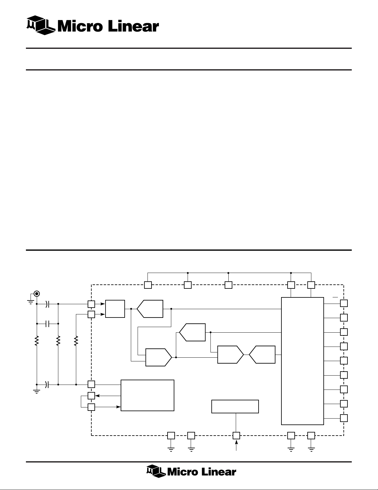
BLOCK DIAGRAM/TYPICAL APPLICATION *Some Packages Are End Of Life
VIDEO
INPUT
75Ω
47µF
0.1µF
10µF
5V
VDD
A
+
+
VIN+
150MHz
T & H
–
V
IN
1kΩ1kΩ
VIN
-BIAS
VREF
VREF
OUT
IN
1.5V
1.0V
ADC 1
SUB
DAC
AMP
INTERNAL
REFERENCES
GND
A
VDD
ADC 2
GND
A
A
VDD
A
SUB
DAC
AMP
CLOCK GENERATOR
CLK
20MHz
ADC 3
VDD
GND
D
DIGITAL
ERROR
CORRECTION
D
VDD
GND
D
OE
D7
D6
D5
D4
D3
D2
D1
D0
O
1
Page 2
ML6401
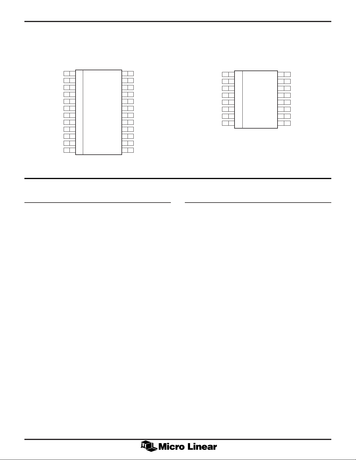
PIN CONFIGURATION
ML6401-1
24-Pin SOIC (S24W)
GND
VDD
OE
D0
D1
D2
D3
D4
D5
D6
D7
CLK
1
O
O
2
3
4
5
6
7
8
9
10
11
12
TOP VIEW
24
23
22
21
20
19
18
17
16
15
14
13
GND
VIN–
V
IN–BIAS
GNDA
GNDA
V
+
IN
VDD
VREF
VREF
VDD
VDD
VDD
D
A
IN
OUT
A
A
D
PIN DESCRIPTION (Pin numbers in parentheses are for S16N package)
PIN NAME DESCRIPTION
1 (16) OE Output Enable. A logic low signal
on this pin enables the outputs.
2 GNDOOutput ground pin.
3 (1) D0 D0 (LSB) output signal (TTL
compatible).
4 (2) D1 D1 output signal (TTL compatible).
PIN NAME DESCRIPTION
13 (9,11) VDD
14 (12) VDD
15 (12) VDD
16 VREF
D0
D1
D2
D3
D4
D5
D6
D7
ML6401-3
16-Pin SOIC (S16N)
1
2
3
4
5
6
7
8
TOP VIEW
Digital supply pin.
D
Analog supply pin.
A
Analog supply pin.
A
Full scale reference output.
OUT
16
15
14
13
12
11
10
9
Connect to pin 17 for self bias.
(VRTS on 1175) (ML401-1 only)
OE
GND
GND
VIN+
VDD
VDD
CLK
VDD
D
A
A
D
D
5 (3) D2 D2 output signal (TTL compatible).
6 (4) D3 D3 output signal (TTL compatible).
7 (5) D4 D4 output signal (TTL compatible).
8 (6) D5 D5 output signal (TTL compatible).
9 (7) D6 D6 output signal (TTL compatible).
10 (8) D7 D7 (MSB) output signal (TTL
compatible).
11 VDDOOutput supply pin.
12 (10) CLK Clock input pin.
17 VREF
Full scale reference input.
IN
Connect to pin 16 for self bias.
(VRT on 1175) (ML401-1 only)
18 (12) VDD
Analog supply pin.
A
19 (13) VIN+ Input signal.
20 (14) GND
21 (14) GND
22 V
IN–BIAS
Analog ground.
A
Analog ground.
A
Common mode bias output.
Connect to pin 23 for self bias.
(VRBS on 1175) (ML401-1 only)
23 VIN– Common mode bias input.
Connect to pin 22 for self bias.
Drive with the negative input if
differential input is being used.
(VRB on 1175)
(ML401-1 only)
24 (15) GND
Digital Ground.
D
2
Page 3

ABSOLUTE MAXIMUM RATINGS
ML6401
Absolute maximum ratings are those values beyond which
the device could be permanently damaged. Absolute
maximum ratings are stress ratings only and functional
device operation is not implied.
Supply Current (ICC) ............................................... 55mA
Peak Driver Output Current ............................... ±500mA
Analog Inputs ...................................................–0.3 to 7V
Junction Temperature ............................................. 150°C
Storage Temperature Range ..................... –65°C to 150°C
Lead Temperature (soldering, 10 sec) ..................... 150°C
Thermal Resistance (θ
)
JA
Plastic DIP ....................................................... 80°C/W
Plastic SOIC ................................................... 110°C/W
OPERATING CONDITIONS
Temperature Range ....................................... 0°C to 70°C
T
PWH(min)
= T
PWL(min)
............................................... 25ns
ELECTRICAL CHARACTERISTICS
Unless otherwise specified, CL = 15pF, V
PARAMETER CONDITIONS MIN TYP MAX UNITS
Resolution 8 Bits
Power Dissipation 200 325 mW
Transfer Function
DC Integral Linearity f
DC Differential Linearity f
AC Integral Linearity V
Offset Voltage VIN– = V
Gain Error VIN– = V
Analog Signal Processing
= 5V ±10%, T
CC
= 15MSPS ±0.8 ±1.25 LSB
CLk
= 15MSPS ±0.6 ±1 LSB
CLk
= 2V, 4.4MHz ±2 LSB
IN
IN–BIAS
IN–BIAS
= Operating Temperature Range (Note 1).
A
, VREF
, VREF
OUT
OUT
= VREF
= VREF
IN
IN
±10 LSB
±2 ±5 LSB
Differential Gain V
Differential Phase V
Signal to Noise Ratio VIN = 2V, 1MHz, f
= NTSC 40 IRE modulated ramp,
IN
f
= 14.3 MSPS 1.8 %
CLK
= NTSC 40 IRE modulated ramp,
IN
f
= 14.3 MSPS 0.9 degree
CLK
= 20MHz 48 dB
CLK
Distortion 0.18 %
Spurious Free Dynamic Range 58 dB
SIN and Distortion (SINAD) 47 dB
Effective Bits 7.4 bits
Analog Inputs
Input Voltage Digital Output = 0,
VIN– = V
IN–BIAS
, VREF
OUT
= VREF
IN
0.5 V
Digital Output = 255,
Input Current f
VIN– = V
= 20MHz ±20 ±30 µA
CLK
IN–BIAS
, VREF
OUT
= VREF
IN
2.5 V
Input Capacitance VIN = 2V 4.0 pF
Analog Input Bandwidth 150 MHz
Reference Outputs
V
IN–BIAS
VREF
V
RIN
OUT
IREF
= 50µA 0.97 1.0 1.03 V
OUT
1.45 1.5 1.55 V
±5 µA
3
Page 4

ML6401
ELECTRICAL CHARACTERISTICS (Continued)
PARAMETER CONDITIONS MIN TYP MAX UNITS
Switching Characteristics
Maximum CLK Input Frequency 20 25 MHz
Clock Duty Cycle CLK = 13.5MHz 40 60 %
t
PWH
t
PWL
CLK ≤ 20MHz 25 ns
CLK ≤ 20MHz 25 ns
Analog To Digital Converter Inputs — CLK
Low Level Input Voltage V
High Level Input Voltage V
Low Level Input Current V
IL
IH
= 0.1V –5 +5 µA
IL
High Level Input Current VIH = VDD
– 0.1V –5 +5 µA
D
0 0.8 V
2.4 VDD
D
Input Capacitance 4.0 pF
Timing — Digital Outputs (CL = 15pF, IOL = 2mA, R
Sampling Delay t
Output Hold Time t
Output Delay Time t
DS
HO
DO
= 2kΩ, f
L
= 20MHz)
CLK
5ns
41210ns
51830ns
Three-State Delay Time — Output Enable 10 25 ns
Three-State Delay Time — Output Disable 10 20 ns
Analog To Digital Converter Outputs — Digital
Low Level Output Voltage IOL = 2mA 0 0.6 V
High Level Output Voltage IOH = 2mA 2.4 VCC
O
Output Current in Three-State Mode –20 +20 µA
Supplies
V
V
Analog, Digital & Output Supply Voltage 4.5 5.5 V
Analog Supply Current Static 26 34 mA
Digital Supply Current f
Output Supply Current f
Note 1: Limits are guaranteed by 100% testing, sampling, or correlation with worst-case test conditions.
TIMING DIAGRAM
SAMPLE
(VIN+) – (VIN–)
CLK
D0 TO D7
N
N–3 N–2 N–1 N N+1
= 20MHz 10 15 mA
CLK
= 20MHz, CL = 0pF 4 10 mA
CLK
N+1
t
DS
t
HO
t
DO
N+2 N+3
OUT
t
PWH
N+4
t
PWL
4
Page 5

FUNCTIONAL DESCRIPTION
ML6401
INTRODUCTION
The Micro Linear ML6401 is a single-chip video A/D
converter IC which is intended for analog to digital
conversion of 2Vp-p signals at rates up to 20MSPS.
Incorporating both bias and clock generation, it forms a
complete solution for data conversion. The operating
power dissipation is typically less than 200mW. The IC is
designed to offer low power dissipation and a high level
of integration resulting in an optimized solution. The IC
consists of an input track and hold, a three stage pipelined
A/D converter, digital error correction circuitry, internal
dual non-overlapping clock generator, and internal
voltage reference.
INPUT TRACK AND HOLD
The input track and hold consists of a differential
capacitor feedback amplifier. The input capacitance,
including pin protection and transmission gate, is 4pF.
The input to the track and hold can be driven differentially,
or single-ended. Single-ended operation uses an internal
or external reference to bias the negative input. The full
scale range can be set externally, or supplied from an
internal source. The track and hold samples the input
signal during the positive half cycle of the input clock,
and holds the last value of VIN during the negative half
cycle of the input clock. The settling time of the amplifier
is less than 20ns.
8
A/D CONVERTER
The A/D conversion is performed via a three stage
pipelined architecture. The first two stages quantize their
input signal to three bits, then subtract the result from the
input and amplify the difference by a factor of four. This
creates a residue signal which spans the full scale range of
the following converter. The subtraction and amplification
is performed via a differential capacitor feedback
amplifier, similar to the input track and hold. The third
stage quantizes the signal to four bits. One bit from each
of the last two stages is used for error correction.
The first stage A/D performs the conversion at the end of
the track and hold period, approximately one-half cycle
after the input was sampled. The second stage A/D
performs the conversion one half cycle later, after the
subtraction/amplification of the first stage has settled. The
third stage A/D performs the conversion after another onehalf cycle delay, when the second stage has settled. Error
correction is then performed, and, one clock cycle later,
data is transferred to the output latch. This permits the
data to be read 3 clocks after the sample was taken.
This technique results in lower input capacitance, lower
harmonic distortion, and higher signal to noise ratios than
the classical two step parallel technique, providing a
greater number of effective bits.
CLOCK GENERATION
The ML6401 typically requires an input clock that if
running at 20MHz would have a low time of 25ns, and a
high time of 25ns. This input is applied to a clock
generation circuit which creates the two non-overlapping
clock signals required by the feedback amplifiers.
Pipeline delay is the number of clock cycles between
conversion initiation and the associated output data being
made available. New output data is provided every clock
cycle.
7
EFB
6
12345678910
FREQUENCY
Typical Effective Bits versus Input Signal Frequency.
5
Page 6

ML6401
INPUT COUPLING
The following two figures illustrate two simple means
of connecting AC and DC coupled signals into the
ML6401-1.
CXD1175 REPLACEMENT
The 24-pin ML6401-1 is pin compatible with the Sony
CXD1175 since all features common to both A/D’s share
common pins. The 24-pin ML6401-1 is not, however, a
direct replacement for the CXD1175. The architectural
differences between the two parts result in slightly
different application circuits only in the area of the
reference pins.
The 1175 brings the top and bottom of the reference
ladder to external pins (denoted VRT and VRB
respectively), and provides two additional pins (VRTS and
VRBS) which can be used to bias the ladder. There are
three major differences in the use of the 24-pin ML6401-
1. First, there is no single resistor ladder which can be
brought out to users in order to vary gain and offset.
Second, the 24-pin ML6401 cannot handle full scale
ranges of VDDA volts. And third, where the 1175
architecture has two voltages (VRT and VRB) which fix the
two endpoints of the conversion range (code 255 and
code 0), the 24-pin ML6401 has one voltage (VREF) which
affects only full scale range (code 255 – code 0) and one
voltage (VIN–) which affects only bias (code 128). An
internally generated VREF
(VRTS of 1175), and an internally generated V
(1 volt) is brought to pin 16
OUT
IN-BIAS
(1.5
volts) is brought to pin 22 (VRBS of 1175). This allows the
following four modes of operation:
1. CXD1175 — See Figure 3. Connect VRTS to VRT and
VRBS to VRB. The ladder will have 2 volts across it
(equal to the full scale range), which varies with supply.
ML6401 — With pin 16 connected to pin 17, and pin
22 connected to pin 23, the A/D will supply internally
generated bandgap biases, making full scale range 2
volts and bias (code 128) 1.5 volts. This is a virtual
drop in for an 1175 with pins 16 and 17 shorted, and
pins 22 and 23 shorted (0.1 volt bias difference).
2. CXD1175 — See Figure 4. Leave VRTS and VRBS open,
and drive VRT and VRB with external voltages. The
1175 spec allows VRT-VRB to equal from 1.8 volts to
VDDA volts. This allows users the flexibility to supply
higher quality references (higher precision, lower
noise), and change the full scale range of the A/D (these
voltages can be varied to effectively implement a VGA).
Also, the offset of the A/D can be varied.
ML6401 — Leave pin 16 and pin 22 open, and drive
pin 17 and pin 23 with external voltages. The full scale
range will be 2 × pin 17 volts, and the bias (code 128)
will occur at pin 23 ±2% volts. The full scale range of
the A/D must be kept below 4 volts, but the part is only
specified for full scale range of 2 volts.
VIDEO
INPUT
R
L
75Ω
47µF
0.1µF
0.01µF
10µF
+
VIDEO
INPUT
R
R
A
–0.5V to +0.5V
A
+0.5V to 2.5V
+
3 × R
R
A
R
= 1k TYP
A
0.01µF
A
0.01µF
VIN+
V
IN
V
IN-BIAS
VREF
VREF
VDD
A
ADC 1S & H
–
1.5V
OUT
IN
1.0V
INTERNAL
REFERENCES
GND
D
VDD
A
+
R
R
B
B
VIN+
ADC 1S & H
–
V
IN
1kΩ1kΩ
V
IN-BIAS
VREF
VREF
OUT
IN
1.5V
1.0V
INTERNAL
REFERENCES
GND
D
Figure 1. AC Coupled Input, External Resistors
Bias the Input.
6
Figure 2. DC Coupled Input.
Page 7

ML6401
+12V
Q1
R4
1kΩ
R3
500Ω
C3
47µF
Q2
+
R5
2kΩ
+
+
C6
47µF
C1
470µF
+
V
IN
R1
120Ω
*POT R7 WILL HAVE TO BE ADJUSTED
Note: Circuit in dashed lines is an optional 1175 input
network which can be replaced with circuits in
Figure 1 or 2.
C5
0.1µF
R2
180Ω
–12V
C2
10µF
C4
0.1µF
R7*
5kΩ
POT
R8
100Ω
Q3
R9
5kΩ
C12
0.1µF
R10
75Ω
47µF
C8
0.1µF
C7
47µF
C9
HC04
CLOCK IN
+
C10
0.1µF
+5V
1175 PINOUT
13
VDD
D
14
VDD
A
15
VDD
A
16
VRTS
17
VRT
18
VDD
A
19
C13
10pF
+
C11
0.1µF
VIN+
20
GND
A
21
GND
A
22
VRBS
23
VRB
24
GND
D
VDD
GND
CLK
D7
D6
D5
D4
D3
D2
D1
D0
OE
12
11
O
10
9
8
7
6
5
4
3
2
O
1
CLK
MSB
LSB
Figure 3. Replacement for 1175.
3. CXD1175 — Connect VRBS to VRB and leave VRTS
open while driving VRT with an external voltage. This
allows similar functionality to #2 preceding, but the
bias voltage (code 0) will move when the full scale
range is changed.
ML6401 — Open pin 16, drive pin 17 externally, and
connect pin 22 to pin 23. The full scale range will be
2 × pin 17 volts, and the bias (code 128) will occur at
1.5 volts (internally generated from bandgap). The full
scale range of the A/D must be kept below 4 volts, but
the part is only specified for full scale range of 2 volts.
4. CXD1175 — Connect VRTS to VRT and leave VRBS
open while driving VRB with an external voltage. This
allows similar functionality to #2 preceding, but the
bias voltage (code 0) will move when the full scale
range is changed.
ML6401 — Connect pin 16 to pin 17, open pin 22 and
drive pin 23 externally. The full scale range will be 2
volts (internally generated from bandgap), and the bias
(code 128) will occur at pin 23 ±2% volts.
7
Page 8

ML6401
(1) Sony: A to C, B to D
(2) Micro Linear: A to D, B to C
+12V
+
C6
47µF
C1
470µF
+
V
IN
R1
120Ω
*POT R7 WILL HAVE TO BE ADJUSTED
C5
0.1µF
Q1
R2
180Ω
R4
1kΩ
–12V
R12
1kΩ
R13
500Ω
R3
500Ω
C3
47µF
Q2
R11
1kΩ
(1)
C
D
+
C2
10µF
R5
2kΩ
+
C4
0.1µF
(2)
(2)
(1)
A
B
R8
100Ω
Q3
R7*
5kΩ
POT
R9
5kΩ
C12
0.1µF
+
–
–
+
µPC254
µPC254
47µF
R10
75Ω
C9
+
C8
0.1µF
C7
47µF
Q4
Q5
HC04
CLOCK IN
C10
0.1µF
+5V
1175 PINOUT
13
VDD
D
14
VDD
A
15
VDD
A
16
VRTS
17
VRT
18
VDD
A
19
C13
10pF
+
C11
0.1µF
VIN+
20
GND
A
21
GND
A
22
VRBS
23
VRB
24
GND
D
VDD
GND
CLK
D7
D6
D5
D4
D3
D2
D1
D0
OE
12
11
O
10
9
8
7
6
5
4
3
2
O
1
CLK
MSB
LSB
Note: Circuit in dashed lines is an optional 1175 input
network which can be replaced with circuits in
Figure 1 or 2.
Figure 4. Replacement with Wiring Changes (shown) for the 1175.
8
Page 9

PHYSICAL DIMENSIONS inches (millimeters)
0.600 - 0.614
24
(15.24 - 15.60)
ML6401
Package: S24
24-Pin SOIC
0.024 - 0.034
(0.61 - 0.86)
(4 PLACES)
0.090 - 0.094
(2.28 - 2.39)
0.291 - 0.301
(7.39 - 7.65)
PIN 1 ID
1
0.050 BSC
(1.27 BSC)
0.012 - 0.020
(0.30 - 0.51)
0.095 - 0.107
(2.41 - 2.72)
SEATING PLANE
0.398 - 0.412
(10.11 - 10.47)
0.005 - 0.013
(0.13 - 0.33)
0º - 8º
0.022 - 0.042
(0.56 - 1.07)
0.009 - 0.013
(0.22 - 0.33)
Package: S16N
16-Pin Narrow SOIC
0.386 - 0.396
16
(9.80 - 10.06)
0.017 - 0.027
(0.43 - 0.69)
(4 PLACES)
0.055 - 0.061
(1.40 - 1.55)
1
PIN 1 ID
0.050 BSC
(1.27 BSC)
0.012 - 0.020
(0.30 - 0.51)
0.148 - 0.158
(3.76 - 4.01)
0.059 - 0.069
(1.49 - 1.75)
SEATING PLANE
0.228 - 0.244
(5.79 - 6.20)
0.004 - 0.010
(0.10 - 0.26)
0º - 8º
0.015 - 0.035
(0.38 - 0.89)
0.006 - 0.010
(0.15 - 0.26)
11
Page 10

ML6401
ORDERING INFORMATION
PART NUMBER TEMPERATURE RANGE PACKAGE
ML6401CS-1 0°C to 70°C 24-Pin SOIC (S24)
ML6401CS-30°C to 70°C16-Pin SOIC (S16N) (EOL)
© Micro Linear 1997 is a registered trademark of Micro Linear Corporation
Products described in this document may be covered by one or more of the following patents, U.S.: 4,897,611; 4,964,026; 5,027,116; 5,281,862; 5,283,483; 5,418,502; 5,508,570; 5,510,727; 5,523,940;
5,546,017; 5,559,470; 5,565,761; 5,592,128; 5,594,376; Japan: 2598946. Other patents are pending.
Micro Linear reserves the right to make changes to any product herein to improve reliability, function or design.
Micro Linear does not assume any liability arising out of the application or use of any product described herein,
neither does it convey any license under its patent right nor the rights of others. The circuits contained in this
data sheet are offered as possible applications only. Micro Linear makes no warranties or representations as to
whether the illustrated circuits infringe any intellectual property rights of others, and will accept no responsibility
or liability for use of any application herein. The customer is urged to consult with appropriate legal counsel
before deciding on a particular application.
10
2092 Concourse Drive
San Jose, CA 95131
Tel: 408/433-5200
Fax: 408/432-0295
DS6401-01
 Loading...