

Page 1
July 2000
PRELIMINARY
ML4832*
Electronic Dimming Ballast Controller
GENERAL DESCRIPTION
The ML4832 is a complete solution for a dimmable/nondimmable, high power factor, high efficiency electronic
ballast. The BiCMOS ML4832 contains controllers for
“boost” type power factor correction as well as for a
dimming ballast.
The power factor circuit uses the average current sensing
method with a gain modulator and overvoltage protection.
This system produces a power factor of better than 0.99
with low input current THD at > 95% efficiency. Special
care has been taken in the design of the ML4832 to
increase system noise immunity by using a high amplitude
oscillator, and a current-fed multiplier. An overvoltage
protection comparator inhibits the PFC section in the
event of a lamp out or lamp failure condition.
The ballast section provides for programmable starting
scenarios with programmable preheat and lamp out-ofsocket interrupt times. The IC controls lamp output through
frequency modulation using lamp current feedback.
FEATURES
■ Complete power factor correction and dimming
ballast control in one IC
■ Low distortion, high efficiency continuous boost,
average current sensing PFC section
■ Programmable start scenario for rapid or instant
start lamps
■ Lamp current feedback for dimming control
■ Variable frequency dimming and starting
■ Programmable restart for lamp out condition to
reduce ballast heating
■ Over-temperature shutdown replaces external
heat sensor for safety
■ PFC overvoltage comparator eliminates output
“runaway” due to load removal
■ Large oscillator amplitude and gain modulator
improves noise immunity
■ Low start-up current <0.5mA
(* Indicates part is End Of Life as of July 1, 2000)
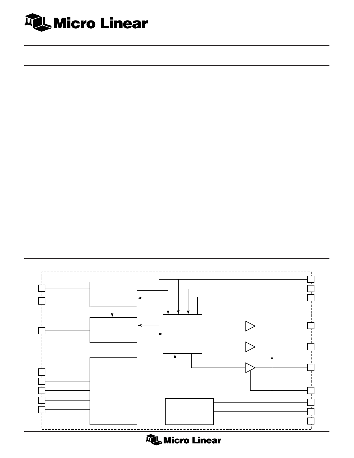
BLOCK DIAGRAM
R
SET
7
R
T/CT
8
R
X/CX
10
IA OUT
2
IA+
4
I
SINE
3
EA OUT
1
EA–/OVP
18
VARIABLE FREQUENCY
OSCILLATOR
PRE-HEAT
AND INTERRUPT
TIMERS
POWER
FACTOR
CONTROLLER
CONTROL
&
GATING LOGIC
UNDER-VOLTAGE
AND THERMAL
SHUTDOWN
OUTPUT
DRIVERS
INTERRUPT
LAMP FB
LFB OUT
OUT A
OUT B
PFC OUT
PGND
V
V
REF
GND
9
5
6
14
13
15
12
CC
16
17
11
1
Page 2
ML4832
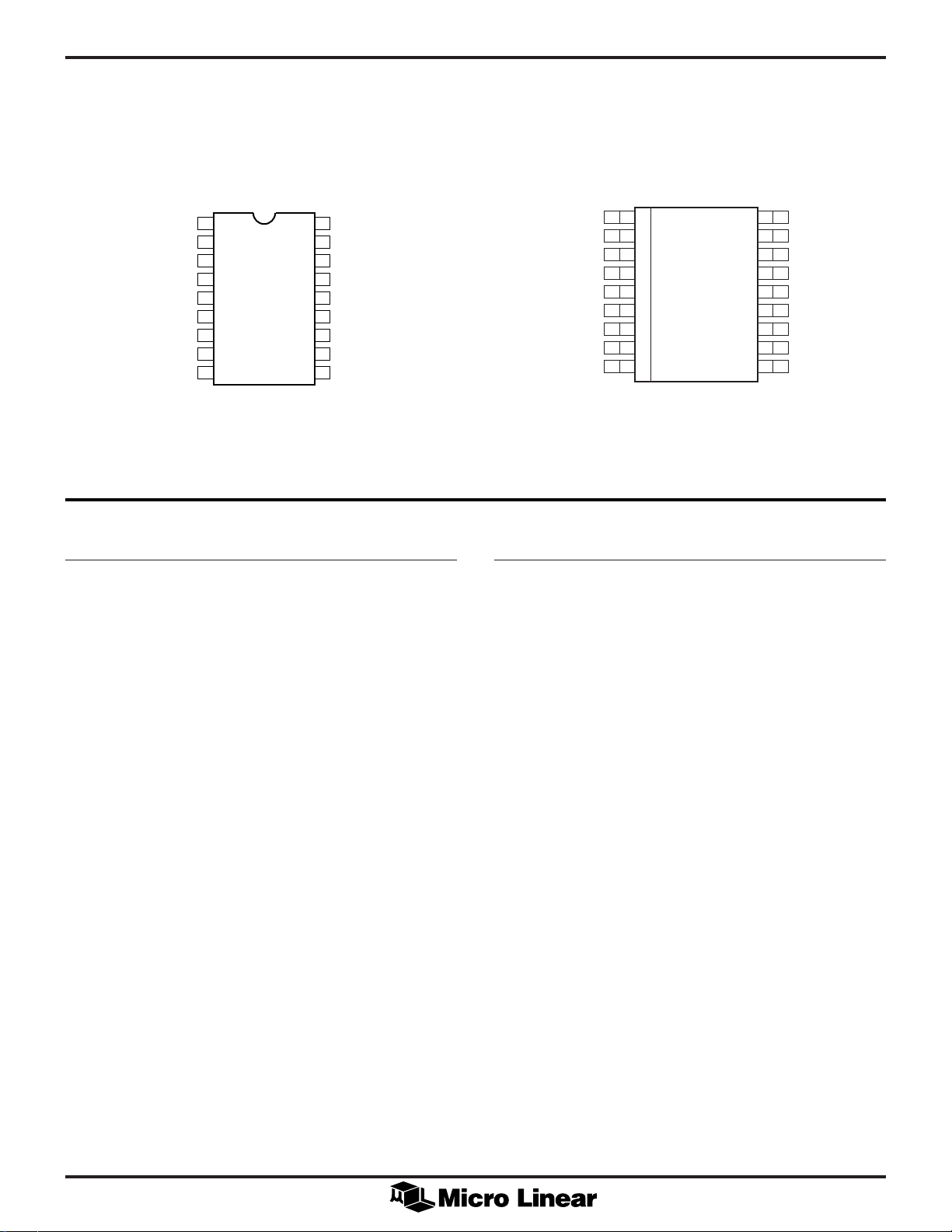
PIN CONFIGURATION
ML4832
18-Pin SOIC (S18)
1
2
3
4
5
6
7
8
9
TOP VIEW
EA OUT
IA OUT
I
SINE
IA+
LAMP FB
LFB OUT
R
SET
RT/C
INTERRUPT
ML4832
18-Pin DIP (P18)
1
2
3
4
5
6
7
8
T
9
TOP VIEW
18
EA–/OVP
17
V
REF
V
16
CC
PFC OUT
15
OUT A
14
OUT B
13
P GND
12
GND
11
R
10
X/CX
EA OUT
IA OUT
I
SINE
IA+
LAMP FB
LFB OUT
R
SET
RT/C
INTERRUPT
T
PIN DESCRIPTION
PIN# NAME FUNCTION PIN# NAME FUNCTION
1 EA OUT PFC error amplifier output and
compensation node
2 IA OUT Output and compensation node of the
PFC average current transconductance
amplifier
3I
SINE
PFC gain modulator input
9 INTERRUPT Input used for lamp-out detection
and restart. A voltage greater than
7.5 volts resets the chip and
causes a restart after a
programmable interval.
10 RX/C
X
Sets the timing for the preheat,
dimming lockout, and interrupt
18
17
16
15
14
13
12
11
10
EA–/OVP
V
REF
V
CC
PFC OUT
OUT A
OUT B
P GND
GND
R
X/CX
4 IA+ Non-inverting input of the PFC average
current transconductance amplifier
and peak current sense point of the
PFC cycle by cycle current limit
comparator
5 LAMP FB Inverting input of an error amplifier
used to sense (and regulate) lamp arc
current. Also the input node for
dimming control.
6 LFB OUT Output from the lamp current error
transconductance amplifier used for
lamp current loop compensation
7R
SET
8RT/C
T
External resistor which sets oscillator
F
, and RX/CX charging current
MAX
Oscillator timing components
11 GND Ground
12 P GND Power ground for the IC
13 OUT B Ballast MOSFET drive output
14 OUT A Ballast MOSFET drive output
15 PFC OUT Power Factor MOSFET drive
output
16 V
17 V
CC
REF
Positive supply for the IC
Buffered output for the 7.5V
voltage reference
18 EA–/OVP Inverting input to PFC error
amplifier and OVP comparator
input
2
Page 3
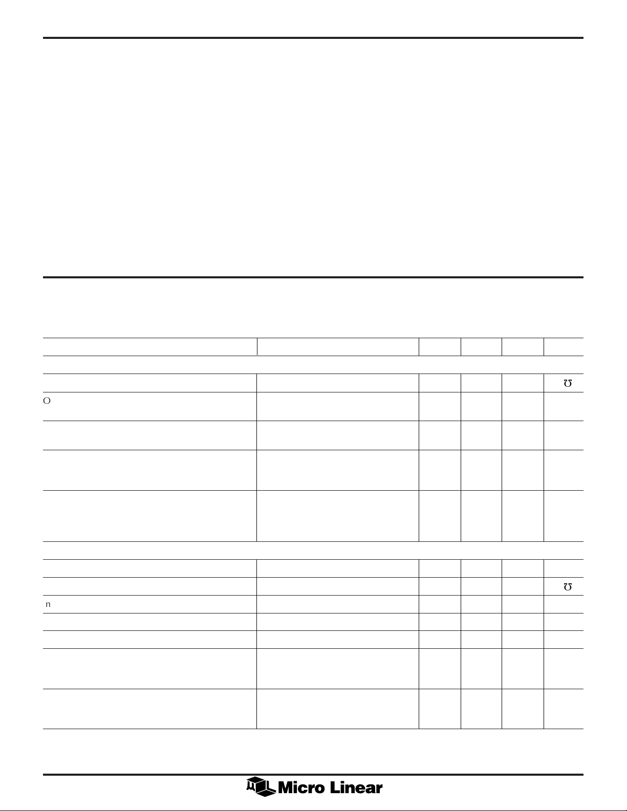
ABSOLUTE MAXIMUM RATINGS
ML4832
Absolute maximum ratings are those values beyond which
the device could be permanently damaged. Absolute
maximum ratings are stress ratings only and functional
device operation is not implied.
Maximum Forced Voltage
(IA OUT)................................................. –0.3V to 7.5V
Junction Temperature ............................................. 150°C
Storage Temperature Range...................... –65°C to 150°C
Lead Temperature (Soldering 10 sec.) ..................... 260°C
Supply Current (ICC) ............................................... 60mA
Output Current, Source or Sink (OUT A, OUT B, PFC
OUT)
Thermal Resistance (qJA)
Plastic PDIP ..................................................... 70°C/W
Plastic SOIC................................................... 100°C/W
DC ................................................................... 250mA
Output Energy (capacitive load per cycle)............... 1.5mJ
Gain Modulator I
Input .....................................10mA
SINE
Analog Inputs ....................................... –0.3V to VCC –2V
IA+ Input Voltage.............................................. –3V to 2V
OPERATING CONDITIONS
Temperature Range
ML4832C ..................................................0°C to 85°C
Maximum Forced Voltage
(EA OUT, LFB OUT) ................................ –0.3V to 7.7V
Maximum Forced Current
(EA OUT, IA OUT, LFB OUT) ............................±20mA
ELECTRICAL CHARACTERISTICS
Unless otherwise specified, R
TA = Operating Temperature Range (Note 1)
PARAMETER CONDITIONS MIN TYP MAX UNITS
PFC CURRENT SENSE AMPLIFIER
Small Signal Transconductance 40 90 120 µ
= 22.1kW, RT = 15.8kW, CT = 1.5nF, C(VCC) = 1µF, I
SET
= 200µA, VCC = 12.5V,
SINE
W
Output Low I
Output High I
Source Current I
Sink Current I
PFC VOLTAGE FEEDBACK AMPLIFIER/LAMP CURRENT AMPLIFIER
Input Bias Current –0.3 –1.0 µA
Small Signal Transconductance 30 55 90 µ
Input Voltage Range –0.3 5.0 V
Output Low V
Output High V
Source Current V
= 0mA, V
SINE
V
= –0.3V, RL = ¥ 0.2 0.4 V
IA+
= 1.5mA, 6.3 6.8 V
SINE
V
SINE
V
V
SINE
V
V
TJ = 25ºC 0.03 0.07 0.16 mA
V
TJ = 25ºC
= V
EA–/OVP
= 1.5mA, –0.05 –0.15 –0.25 mA
EA–/OVP
IA OUT
= 0mA, V
= –0.6V
IA+
EA OUT
LAMP FB
LAMP FB
LAMP FB
EA OUT
IA+
= V
IA+
= 6V, TJ = 25ºC
= 0V, V
= V
EA–/OVP
= V
EA–/OVP
= V
EA–/OVP
= V
LFB OUT
= 0V,
EA OUT
= 0V, RL = ¥
= 0V,
= 0.3V,
IA OUT
= 5V,
EA–/OVP
= 3V, RL = ¥ 0.2 0.4 V
= 2V, RL = ¥ 7.1 7.5 7.8 V
= 0V, –0.06 –0.15 –0.30 mA
= 7V,
W
Sink Current V
LAMP FB
V
EA OUT
TJ = 25ºC
= V
= V
EA–/OVP
LFB OUT
= 5V, 0.06 0.12 0.28 mA
= 0.3V,
3
Page 4
ML4832
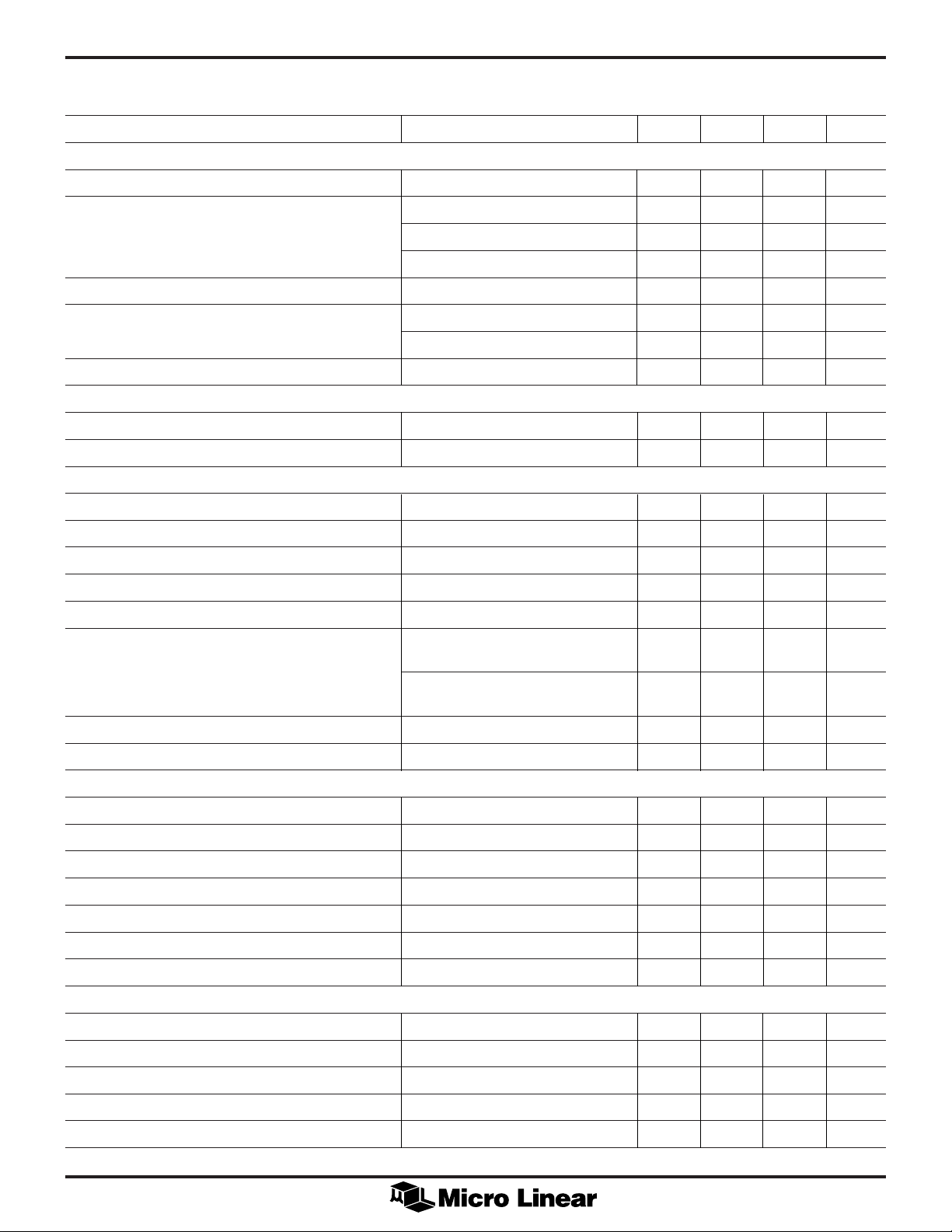
ELECTRICAL CHARACTERISTICS (Continued)
PARAMETER CONDITIONS MIN TYP MAX UNITS
GAIN MODULATOR
Output Voltage (V
Output Voltage Limit I
Offset Voltage I
I
Input Voltage I
SINE
)I
MUL
= 100µA, V
SINE
I
= 300µA, V
SINE
I
=100µA, V
SINE
I
= 300µA, V
SINE
= 1.5mA, V
SINE
= 0µA, V
SINE
I
= 150µA, V
SINE
= 200µA 0.8 1.4 1.8 V
SINE
EA–/OVP
= 3V 85 mV
EA OUT
= 3V 260 mV
EA OUT
= 6V 200 mV
EA OUT
= 6V 600 mV
EA OUT
= 0V 0.9 1 1.1 V
EA–/OVP
= 0V 15 mV
= 3V 15 mV
EA–/OVP
PFC CURRENT — LIMIT COMPARATOR
Current-Limit Threshold –0.85 –1.0 –1.15 V
Propagation Delay 100mV step and 100mV overdrive 100 ns
OSCILLATOR
Initial Accuracy TA = 25°C 72 76 80 kHz
Voltage Stability V
– 4.0V < VCC < V
CCZ
– 0.5V 1 %
CCZ
Temperature Stability 2%
Total Variation Line, temperature 69 83 kHz
Ramp Valley to Peak 2.5 V
C
Charging Current V
T
V
V
= 3V, V
LAMP FB
= 0.9V (Preheat) –90 –113 –130 µA
RX/CX
= 3V, V
LAMP FB
RT/CT
RT/CT
= 2.5V,
= 2.5V,
RX/CX = Open –180 –230 –260 µA
CT Discharge Current V
= 2.5V 4.0 5.5 7.0 mA
RT/CT
Output Drive Deadtime 0.64 0.91 1.30 µs
REFERENCE SECTION
Output Voltage TA = 25°C, IO = 1mA 7.4 7.5 7.6 V
Line regulation V
– 4.0V < VCC < V
CCZ
– 0.5V 8 25 mV
CCZ
Load regulation 1mA < IO < 5mA 2 15 mV
Temperature stability 0.4 %
Total Variation Line, load, temp 7.35 7.65 V
Output Noise Voltage 10Hz to 10kHz 50 µV
Long Term Stability TJ = 125°C, 1000 hrs 5 mV
PREHEAT AND INTERRUPT TIMER (RX = 680KW, CX = 4.7µF)
Initial Preheat Period 0.8 s
Subsequent Preheat Period 0.7 s
Start Period 1.2 s
Interrupt Period 5.7 s
Pin 10 Charging Current –24 –28 –33 µA
4
Page 5
ML4832
ELECTRICAL CHARACTERISTICS (Continued)
PARAMETER CONDITIONS MIN TYP MAX UNITS
PREHEAT AND INTERRUPT TIMER (RX = 680KW, CX = 4.7µF) CONTINUIED
Pin 10 Open Circuit Voltage VCC < Start-up threshold 0.4 0.7 1.0 V
Pin 10 Maximum Voltage 7.0 7.3 7.7 V
Input Bias Current V
= 1.2V 0.1 µA
RX/CX
Preheat Lower Threshold 1.05 1.22 1.36 V
Preheat Upper Threshold 4.4 4.77 5.15 V
Interrupt Recovery Threshold 1.05 1.22 1.36 V
Start Period End Threshold 6.05 6.6 7.35 V
INTERRUPT INPUT
Interrupt Threshold 7.15 7.4 7.65 V
Input Bias Current 0.1 µA
R
Voltage 2.4 2.5 2.6 V
SET
OVP COMPARATOR
OVP Threshold 2.65 2.75 2.85 V
Hysteresis 0.20 0.25 0.27 V
Propagation Delay 1.4 µs
OUTPUTS
Output Voltage Low I
Output Voltage High I
Output Voltage Low in UVLO I
= 20mA 0.1 0.2 V
OUT
I
= 200mA 1.0 2.0 V
OUT
= –20mA V
OUT
I
= –200mA V
OUT
= 10mA, VCC 8V 0.2 V
OUT
– 0.2 VCC – 0.1 V
CC
– 2.0 VCC – 1.0 V
CC
Output Rise/Fall Time CL = 1000pF 20 ns
UNDER-VOLTAGE LOCKOUT AND BIAS CIRCUITS
IC Shunt Voltage (V
)I
CCZ
= 15mA 14.2 15.0 15.8 V
CC
Start-up Current VCC = Start-up threshold –0.2V 0.34 0.48 mA
Operating Current VCC = 12.5V, V
EA–/OVP
= V
V
= 0V, 5.5 8.0 mA
IA+
= 2.3V,
LAMP FB
IA OUT = open
RT = 16.2kW, R
= 22.1kW
SET
VCC = 12.5V, CL = 0
Start-up Threshold V
Shutdown Threshold V
– 1.2 V
CC
– 5.5 V
CC
– 1.0 VCC – 0.8 V
CCZ
– 5.0 VCC – 4.5 V
CCZ
Shutdown Temperature (TJ) 120 °C
Hysteresis (TJ) 30 °C
Note 1: Limits are guaranteed by 100% testing, sampling or correlation with worst case test conditions.
5
Page 6

ML4832
FUNCTIONAL DESCRIPTION
OVERVIEW
The ML4832 consists of an average current controlled
continuous boost power factor front end section with a
flexible ballast control section. Start-up and lamp-out retry
timing are controlled by the selection of external timing
components, allowing for control of a wide variety of
different lamp types. The ballast section controls the lamp
power using frequency modulation (FM) with additional
programmability provided to adjust the VCO frequency
range. This allows for the IC to be used with a variety of
different output networks.
POWER FACTOR SECTION
The ML4832 power factor section is an average current
sensing boost mode PFC control circuit which is
architecturally similar to that found in the ML4821. For
detailed information on this control architecture, please
refer to Application Note 16 and the ML4821 data sheet.
GAIN MODULATOR
The ML4832 gain modulator provides high immunity to
the disturbances caused by high power switching. The
rectified line input sine wave is converted to a current via
a series resistor. In this way, small amounts of ground noise
produce an insignificant effect on the reference to the
PWM comparator.
The output of the gain modulator appears on the positive
terminal of the IA amplifier to form the reference for the
current error amplifier. Please refer to Figure 1.
16
I
SINE VEA V
×−0734.
mA
.
(1)
where: I
V
MUL
=
is the current in the dropping resistor,
SINE
VEA is the output of the error amplifier (Pin 1).
The output of the gain modulator is limited to 1.0V.
7
10
16
17
11
2
4
3
1
18
R
SET
RX/C
X
V
CC
V
REF
GND
IA OUT
IA +
–1V
I
SINE
EA OUT
EA –/OVP
UNDER-VOLTAGE
AND THERMAL
SHUTDOWN
7k
+
–V
MUL
7k
–
+
MODULATORS
–
2.5V
+
GAIN
LFB OUT
VARIABLE
FREQUENCY
PREHEAT
TIMER
PWM (PFC)
2.75V
+
–
–
+
OVP
–
+
OSC
R
S
Q
Q
T
Q
+
2.5V
V
REF
LAMP FB
INTERRUPT
PFC OUT
–
+
–
RT/C
OUT A
OUT B
P GND
6
5
9
T
8
15
14
13
12
Figure 1. ML4832 Block Diagram
6
Page 7

FUNCTIONAL DESCRIPTION (Continued)
ML4832
AVERAGE CURRENT AND OUTPUT VOLTAGE
REGULATION
The PWM regulator in the PFC control section will act to
offset the positive voltage caused by the multiplier output
by producing an offsetting negative voltage on the current
sense resistor at IA+. A cycle-by-cycle current limit is
included to protect the MOSFET from high speed current
transients. When the voltage at IA+ goes negative by more
than 1V, the PWM cycle is terminated.
For more information on compensating the average
current and boost voltage error amplifier loops, see
ML4821 data sheet.
OVERVOLTAGE PROTECTION AND INHIBIT
The OVP pin serves to protect the power circuit from
being subjected to excessive voltages if the load should
change suddenly (lamp removal). A divider from the high
voltage DC bus sets the OVP trip level. When the voltage
on EA–/OVP exceeds 2.75V, the PFC transistors are
inhibited. The ballast section will continue to operate.
TRANSCONDUCTANCE AMPLIFIERS
The PFC voltage feedback, PFC current sense, and the
loop current amplifiers are all implemented as operational
transconductance amplifiers. They are designed to have
low small signal forward transconductance such that a
large value of load resistor (R1) and a low value ceramic
capacitor (<1µF) can be used for AC coupling (C1) in the
frequency compensation network. The compensation
network shown in Figure 2 will introduce a zero and a
pole at:
f
ZP
1
==
ππ
RC
2
11 12
f
1
RC
2
(2)
Figure 3 shows the output configuration for the operational
transconductance amplifiers.
A DC path to ground or VCC at the output of the
transconductance amplifiers will introduce an offset error.
IQ –
gmV
18
2.5V
–
+
R1
C1
C2
Figure 2. Compensation Network
CURRENT
MIRROR
IN OUT
gmV
IQ +
IN
2
IN
2
io = gmV
IN
i
O
0
Linear Slope Region
VIN Differential
IN OUT
CURRENT
MIRROR
Figure 3. Output Configuration Figure 4. Transconductance Amplifier Characteristics
7
Page 8

ML4832
FUNCTIONAL DESCRIPTION (Continued)
The magnitude of the offset voltage that will appear at
the input is given by VOS = io/gm. For an io of 1mA and a
gm of 0.05 µmhos the input referred offset will be 20mV.
Capacitor C1 as shown in Figure 2 is used to block the
DC current to minimize the adverse effect of offsets.
Slew rate enhancement is incorporated into all of the
operational transconductance amplifiers in the ML4832.
This improves the recovery of the circuit in response to
power up and transient conditions. The response to large
signals will be somewhat non-linear as the
transconductance amplifiers change from their low to
high transconductance mode. This is illustrated in
Figure 4.
BALLAST OUTPUT SECTION
The IC controls output power to the lamps via frequency
modulation with non-overlapping conduction. This
means that both ballast output drivers will be low during
the discharging time t
OSCILLATOR
The VCO frequency ranges are controlled by the output
of the LFB amplifier. As lamp current decreases, LFB
OUT rises in voltage, causing the CT charging current to
decrease, thereby causing the oscillator frequency to
decrease. Since the ballast output network attenuates
high frequencies, the power to the lamp will be
increased.
The oscillator frequency is determined by the following
equations:
of the oscillator capacitor CT.
DIS
F
=
OSC
and
tRCIn
=
CHG T T
The oscillator’s minimum frequency is set when ICH = 0
where:
F
≅
OSC
This assumes that t
When LFB OUT is high, ICH = 0 and the minimum
frequency occurs. The charging current varies according to
two control inputs to the oscillator:
1. The output of the preheat timer
2. The voltage at LFB OUT
In preheat condition, charging current is fixed at
>> t
CHG
I
CHG PREHEAT
()
1
tt
+
CHG DIS
VIRV
+−
REF CH T TL
VIRV
+−
REF CH T TH
1
RC
×
051.
DIS
TT
.
.
25
=
R
SET
(3)
(4)
(5)
(6)
V
REF
17
I
R
T
R
T/CT
8
C
T
5.5mA
CHG
1.25/3.75
V
REF
CONTROL
CLOCK
+
–
VTH = 3.75V
C
T
VTL = 1.25V
Figure 5. Oscillator Block Diagram and Timing
t
DIS
t
CHG
8
Page 9

/
FUNCTIONAL DESCRIPTION (Continued)
ML4832
In running mode, charging current decreases as the V
PIN6
rises from 0V to VOH of the LAMP FB amplifier. The
highest frequency will be attained when I
is highest,
CHG
which is attained when LFB OUT is at 0V:
I
CHG
()0
=
5
R
SET
(7)
Highest lamp power, and lowest output frequency are
attained when LFB OUT is at its maximum output voltage
(VOH).
In this condition, the minimum operating frequency of the
ballast is set per (5) above.
For the IC to be used effectively in dimming ballasts with
higher Q output networks a larger CT value and lower R
T
value can be used, to yield a smaller frequency excursion
over the control range (V
LFB OUT
set to 5.5mA. Assuming that I
tC
DIS VCO T()
). The discharge current is
>> IRT:
DIS
600
≅×
(8)
IC BIAS, UNDER-VOLTAGE LOCKOUT AND THERMAL
SHUTDOWN
The IC includes a shunt regulator which will limit the
voltage at VCC to 15V (V
). The IC should be fed with
CCZ
a current limited source, typically derived from the ballast
transformer auxiliary winding. When VCC is below
V
– 1.1V, the IC draws less than 0.48mA of quiescent
CCZ
current and the outputs are off. This allows the IC to start
using a “bleed resistor” from the rectified AC line.
To help reduce ballast cost, the ML4832 includes a
temperature sensor which will inhibit ballast operation if
the IC’s junction temperature exceeds 120°C. In order to
use this sensor in lieu of an external sensor, care should be
taken when placing the IC to ensure that it is sensing
temperature at the physically appropriate point in the
ballast. The ML4832’s die temperature can be estimated
with the following equation:
TT P CW
≅××°65
JAD
(9)
STARTING, RE-START, PREHEAT AND INTERRUPT
The lamp starting scenario implemented in the ML4832
is designed to maximize lamp life and minimize ballast
heating during lamp out conditions.
The circuit in Figure 7 controls the lamp starting scenarios:
Filament preheat and lamp out interrupt. CX is charged
with a current of I
/4 and discharged through RX. The
RSET
voltage at CX is initialized to 0.7V (VBE) at power up. The
time for CX to rise to 4.8V is the filament preheat time.
During that time, the oscillator charging current (I
2.5/R
. This will produce a high frequency for filament
SET
CHG
) is
preheat, but will not produce sufficient voltage to ignite
the lamp.
After cathode heating, the inverter frequency drops to
F
causing a high voltage to appear to ignite the lamp.
MIN
If the voltage does not drop when the lamp is supposed to
have ignited, the lamp voltage feedback coming into pin 9
rises to above V
, the CX charging current is shut off and
REF
the inverter is inhibited until CX is discharged by RX to the
1.2V threshold. Shutting off the inverter in this manner
prevents the inverter from generating excessive heat when
VCCZ
V
CC
V
I
CC
ON
V
OFF
5.5mA
0.34mA
RX/C
X
10
C
X
R
t
t
X
6.8
INT
9
V
REF
0.625
R
1.2/4.8
1.2/6.8
–
+
SET
+
–
+
–
HEAT
DIMMING
LOCKOUT
R
Q
S
INHIBIT
Figure 6. Typical VCC and ICC Waveforms when
the ML4832 is Started with a Bleed Resistor from
the Rectified AC Line and Bootstrapped from an
Auxiliary Winding. Figure 7. Lamp Preheat and Interrupt Timers
9
Page 10

ML4832
FUNCTIONAL DESCRIPTION (Continued)
the lamp fails to strike or is out of socket. Typically this
time is set to be fairly long by choosing a large value
of RX.
LFB OUT is ignored by the oscillator until CX reaches 6.8V
threshold. The lamps are therefore driven to full power and
then dimmed. The CX pin is clamped to about 7.5V.
6.8
4.8
R
X/CX
1.2
.65
0
A summary of the operating frequencies in the various
operating modes is shown below.
OPERATING MODE OPERATING FREQUENCY
[F(MAX) to F(MIN)]
Preheat 2
Dimming
Lock-out F(MIN)
DIMMING
CONTROL F(MIN) TO F(MAX)
HEAT
DIMMING
LOCKOUT
INT
INHIBIT
7.5
Figure 8. Lamp Starting and Restart Timing
10
Page 11

TYPICAL APPLICATIONS
ML4832
Figures 9 and 10 show ballast schematics, both nondimming and dimming. These are power-factor corrected
60W ballasts designed to operate two series connected
F32T8 fluorescent lamps. Both Schematics, Figures 9 and
10, are of previously published ML4831 circuits that have
TO CONVERT FROM AN EXISTING NON-DIMMING
ML4831 TO THE ML4832:
Resistors
Change: R4 to 51kW, 1/4 W, 5% carbon film
R6, R7 to 866kW, 1/4 W, 1%, metal film
R7 to 75kW, 1/4 W, 5%, carbon film
R18 to 470W, 1/4 W, 5%, carbon film
R13 to 5.76kW, 1/4 W, 1%, metal film
R14 to 499kW, 1/4 W, 5%, carbon film
Add: R24 75kW, 1/4 W, 5%, carbon film
R22 51W, 1/4 W, 5%, carbon film
R23 100W, 1/4 W, 5%, carbon film
Delete: R9
Capacitors
Change: C5 to 10nF, 63V, 10% ceramic
C7 to 180pF, 100V, 5% ceramic
C11 to 1nF, 100V, 10% ceramic
C12 to 100nF, 100V, 10% ceramic
C18 to 100µF, 16V, 20% electrolytic
C20 to 100µF, 25V, 20% electrolytic
Add: C23 33nF, 50V, 20% ceramic
Magnetics
Change: T1 to TSD-882
been modified for ML4832 compatibility. The value
changes and component additions made for ML4832
compatibility were for different amplifier compensation,
bootstrap/bias and protection and do not effect the validity
of the circuit description, operational information or
equations.
TO CONVERT FROM AN EXISTING DIMMING ML4831
TO THE ML4832:
Resistors
Change: R4 to 51kW, 1/4 W, 5% carbon film
R6, R11 to 866kW, 1/4 W, 1%, metal film
R7 to 75kW, 1/4 W, 5%, carbon film
R18 to 470W, 1/4 W, 5%, carbon film
R13 to 5.76kW, 1/4 W, 1%, metal film
R14 to 499kW, 1/4 W, 5%, carbon film
R26 to 200kW, 1/4 W, 5%, carbon film
Add: R32 75kW, 1/4 W, 5%, carbon film
R30 51W, 1/4 W, 5%, carbon film
R31 100W, 1/4 W, 5%, carbon film
Delete: R9
Capacitors
Change: C5 to 10nF, 63V, 10% ceramic
C7 to 180pF, 100V, 5% ceramic
C25 to 1nF, 100V, 10% ceramic
C12 to 100nF, 100V, 10% ceramic
C24 to 100µF, 16V, 20% electrolytic
C20 to 100µF, 25V, 20% electrolytic
Add: C27 33nF, 50V, 20% ceramic
C26 100nF, 100V, 10% ceramic
Diodes
Delete: D10, D13
Magnetics
Change: T1 to TSD-882
11
Page 12

ML4832
TP4
R
R
Y
Y
B
B
TP5
4
3
219
T3
7
6
8
C9
33nF
C8
4700pF
C22
33nF
C21
0.001µF
D11
IN4148
R16
1kΩ
D8
IN4148
C19
D3
Q2
R20
D12
107
D1
1A
C3
C1*
IRF820
442kΩ
1A
T1
1A
0.15µF
2.2nF
R17
51Ω
3
T2
6
R7
R12
1A
D7
89
1A
D4
C2
Q3
72
75kΩ
442kΩ
Q1
2.5A
1A
D9
1A
D2
2.2nF
IRF820
R13
5.76kΩ
C10
47µF
C20
R11
D5
100µF
R19
R24
R8
1A
C6
C7
C11
C12
C5
2.2nF
180pF
1nF
100nF
10nF
R3
R15
C4
R5
R4
9.1kΩ
C16
C15
C14
C13
324k
0.1µF
100pF
0.22µF
0.22µF
10µF
15.4kΩ
51kΩ
R2
1kΩ
1
R1
TP1
8
C18
D13
0.1A
R6
866kΩ
1.0Ω
1A
D6
1µF
C17
R22
51Ω
100µF
TP2
181716151413121110
R21
5kΩ
R18 470Ω
R23
100Ω
123456789
R10
11.5kΩ
R14
C23
499kΩ
TP3
ML4832
33nF
51Ω
75kΩ
22Ω
866kΩ
12
F1
HOT
L1
220 VAC
NEUTRAL
*Note: Only One Chassis Ground
Figure 9. 220V Non-Dimming Ballast
Page 13

ML4832
R
R
Y
Y
B
B
6
T5
5
110
R28
D8
20kΩ
0.1A
TP4
R17
R23
TP5
R16
R27
200kΩ
TP2
10kΩ
TP1
8
8
C9
15nF
C8
4700pF
C22
0.33µF
1µF
C17
C24
R30
100µF
51
2
1
439
T4
7
6
Q2
2.5A
Q3
2.5A
51Ω
3
T2
6
72
R7
75kΩ
R12
442kΩ
442kΩ
R13
R32
5.76kΩ
R19
51Ω
1
75kΩ
R24
R29
1
8
64.9kΩ
1.3kΩ
3
D11
–
+
2
R26
0.1A
D16
IC1
200kΩ
R20
5.1V
7
4
–
+
5
6
C26
100nF
R22
11kΩ
1µF
C21
10kΩ
C16
100pF
C15
0.22µF
C14
0.22µF
D15
L1
C13
10µF
C10
2.5A
47µF
R8
22Ω
C20
100µF
R11
866kΩ
R1
1A
D5
L2
R6
866kΩ
1.0Ω
1A
D6
R31
R18
100Ω
470Ω
C27
33nF
181716151413121110
R25
5kΩ
123456789
R10
11.5kΩ
ML4832
R4
51kΩ
R14
499kΩ
R3
R2
R15
324kΩ
TP3
C6
2.2nF
C4
C7
C25
C12
C5
3.3µF
180pF
1nF
100nF
10nF
R5
15.4kΩ
220kΩ
4.3kΩ
1A
D7
Q1
1A
T1
107
1A
D1
1A
D3
C1*
2.2nF
F1
89
D2
D4
C3
0.15nF
C2
D9
1A
1A
2.2nF
1A
HOT
220 VAC
NEUTRAL
*Note: Only One Chassis Ground
Figure 10. 220V Dimming Ballast
13
Page 14

ML4832
PHYSICAL DIMENSIONS inches (millimeters)
Package: P18
18-Pin PDIP
0.890 - 0.910
(22.60 - 23.12)
18
0.045 MIN
(1.14 MIN)
(4 PLACES)
0.170 MAX
(4.32 MAX)
0.125 MIN
(3.18 MIN)
18
PIN 1 ID
1
0.449 - 0.463
(11.40 - 11.76)
0.050 - 0.065
(1.27 - 1.65)
0.016 - 0.022
(0.40 - 0.56)
0.100 BSC
(2.54 BSC)
SEATING PLANE
Package: S18
18-Pin SOIC
0.240 - 0.260
(6.09 - 6.61)
0.015 MIN
(0.38 MIN)
0.295 - 0.325
(7.49 - 8.26)
0º - 15º
0.008 - 0.012
(0.20 - 0.31)
14
0.024 - 0.034
(0.61 - 0.86)
(4 PLACES)
0.090 - 0.094
(2.28 - 2.39)
0.291 - 0.301
(7.39 - 7.65)
PIN 1 ID
1
0.050 BSC
(1.27 BSC)
0.012 - 0.020
(0.30 - 0.51)
0.095 - 0.107
(2.41 - 2.72)
SEATING PLANE
0.398 - 0.412
(10.11 - 10.47)
0.005 - 0.013
(0.13 - 0.33)
0º - 8º
0.022 - 0.042
(0.56 - 1.07)
0.009 - 0.013
(0.22 - 0.33)
Page 15

ML4832
ORDERING INFORMATION
PART NUMBER TEMPERATURE RANGE PACKAGE
ML4832CP (End of Life) 0°C to 85°C Molded PDIP (P18)
ML4832CS (Obsolete) 0°C to 85°C SOIC (S18)
© Micro Linear 1999. is a registered trademark of Micro Linear Corporation. All other trademarks are the property of their respective owners.
Products described herein may be covered by one or more of the following U.S. patents: 4,897,611; 4,964,026; 5,027,116; 5,281,862; 5,283,483;
5,418,502; 5,508,570; 5,510,727; 5,523,940; 5,546,017; 5,559,470; 5,565,761; 5,592,128; 5,594,376; 5,652,479; 5,661,427; 5,663,874; 5,672,959;
5,689,167; 5,714,897; 5,717,798; 5,742,151; 5,747,977; 5,754,012; 5,757,174; 5,767,653; 5,777,514; 5,793,168; 5,798,635; 5,804,950; 5,808,455;
5,811,999; 5,818,207; 5,818,669; 5,825,165; 5,825,223; 5,838,723; 5.844,378; 5,844,941. Japan: 2,598,946; 2,619,299; 2,704,176; 2,821,714.
Other patents are pending.
Micro Linear reserves the right to make changes to any product herein to improve reliability, function or design. Micro Linear does not assume any
liability arising out of the application or use of any product described herein, neither does it convey any license under its patent right nor the rights of
others. The circuits contained in this data sheet are offered as possible applications only. Micro Linear makes no warranties or representations as to
whether the illustrated circuits infringe any intellectual property rights of others, and will accept no responsibility or liability for use of any application
herein. The customer is urged to consult with appropriate legal counsel before deciding on a particular application.
02/19/99Printed in U.S.A.
DS4832-01
2092 Concourse Drive
San Jose, CA 95131
Tel: 408/433-5200
Fax: 408/432-0295
15
 Loading...