

Page 1
May 1997
ML4828*
BiCMOS Phase Modulation/Soft Switching Controller
GENERAL DESCRIPTION
The ML4828 is a complete BiCMOS phase modulation
control IC suitable for full bridge soft switching converters.
Unlike conventional PWM circuits, the phase modulation
technique allows for zero voltage switching (ZVS)
transitions and square wave drive across the transformer.
The IC modulates the phases of the two sides of the bridge
to control output power.
The ML4828 can be operated in either voltage or current
mode. Both cycle-by-cycle current limit, integrating fault
detection, and soft start reset are provided. The undervoltage lockout circuit features a 1.5V hysteresis with a
low starting current to allow off-line start up with a bleed
FEATURES
■ 5V BiCMOS for low power and high frequency
(1MHz) operation
■ Full bridge phase modulation zero voltage switching
circuit with independent programmable delay times
■ Current or voltage mode operation capability
■ Cycle-by-cycle current limiting with integrating fault
detection and restart delay
■ Can be externally synchronized
■ Four 3Ω CMOS output drivers
■ Under-voltage lockout circuit with 1.5V hysteresis
resistor. A shutdown function powers down the IC, putting
it into a low quiescent state.
The circuit can be operated at frequencies up to 1MHz.
The ML4828 contains four high current CMOS outputs
which feature high slew rate with low cross conduction. *Some Packages Are End Of Life
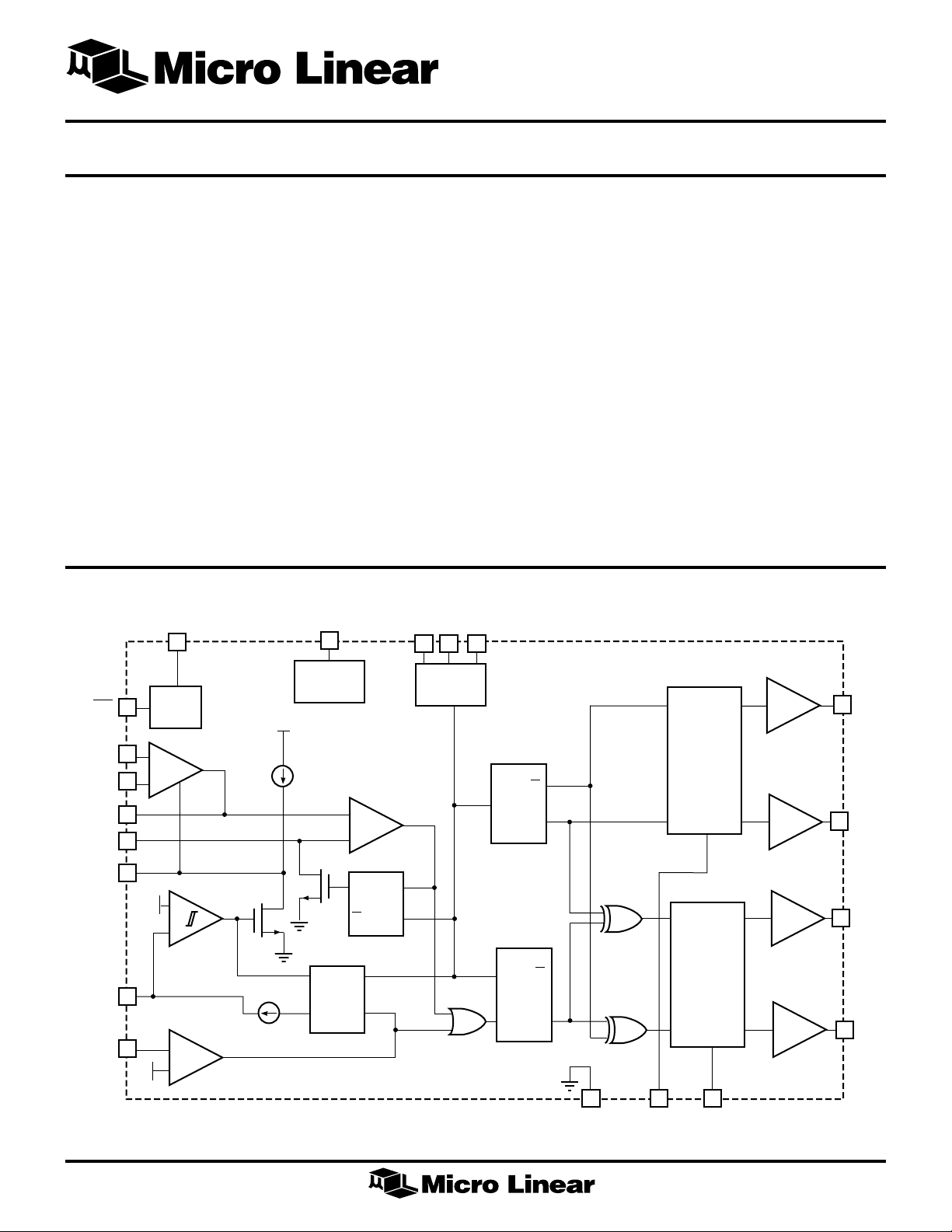
BLOCK DIAGRAM
V
V
CC
14
REF
5
SYNC RTC
643
T
2.5V REF
SDN DRIVER
EA+
EA–
EAO
RAMP
SS
RST
I
LIM
19
10
9
8
11
7
1.25V
12
20
2.5V
1V
+
–
UVLO
+
–
+
–
ERROR
AMP
I
LIM
IRST
ISS
FAULT
LOGIC
–
+
Q
Q
ΦMOD
S
R
OSC
DELAY A
Q
T
Q
Q
R
Q
S
GND
DELAY B
1
R
A
217
R
B
DRIVER
DRIVER
DRIVER
A1
18
A2
16
B1
15
13
B2
1
Page 2
ML4828
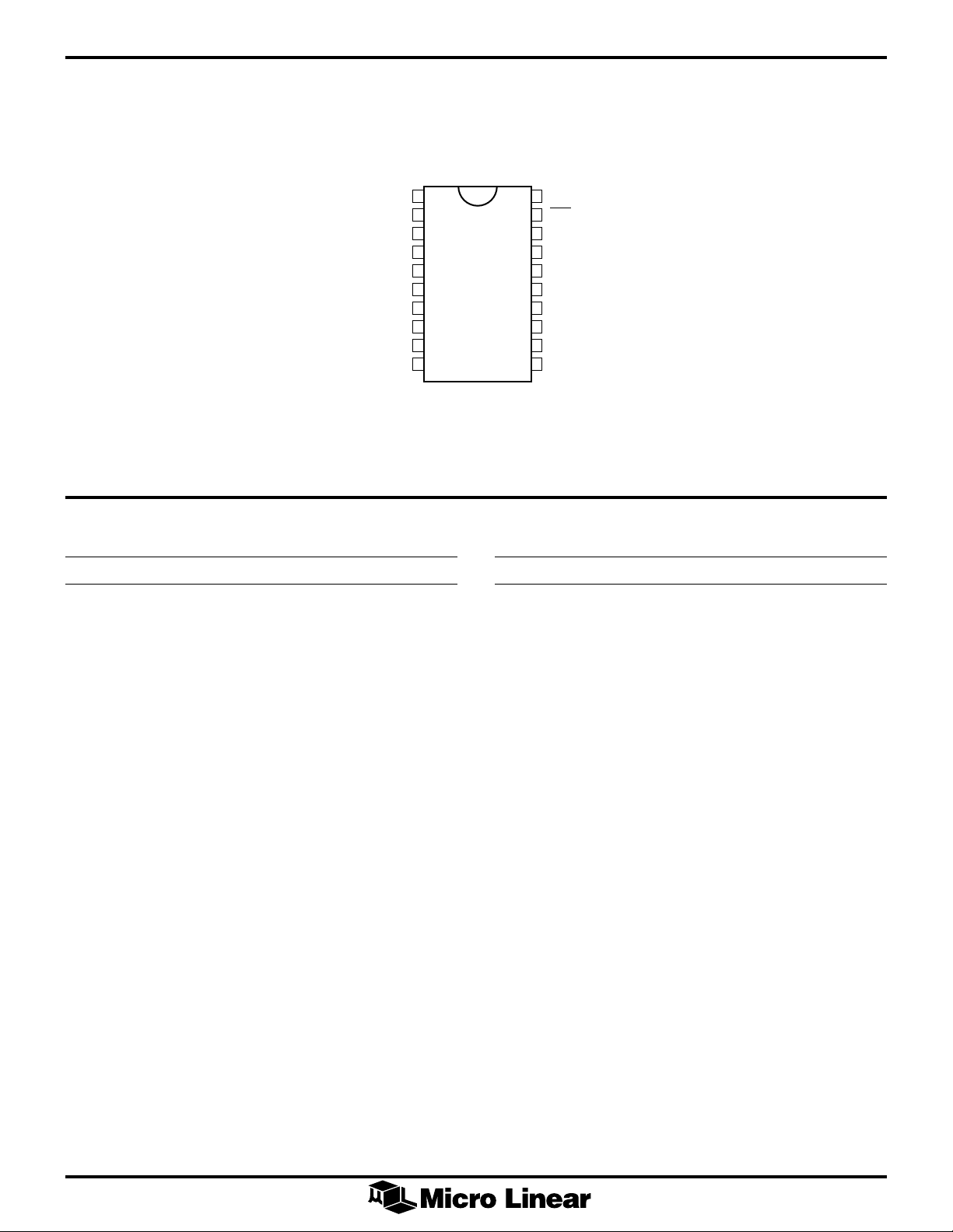
PIN CONNECTION
ML4828
20-Pin DIP (P20)
20-Pin SOIC (S20)
1
RA
2
R
B
3
R
T
4
C
T
5
REF
EA0
EA–
EA+
6
7
SS
8
9
10
TOP VIEW
SYNC
I
LIM
SDN
A1
GND
A2
B1
V
CC
B2
RST
RAMP
20
19
18
17
16
15
14
13
12
11
PIN DESCRIPTION
PIN NAME DESCRIPTION
1R
A
2R
B
3R
T
4C
T
5 REF 2.5V reference voltage.
6 SYNC Synchronization input to oscillator.
7 SS Soft start capacitor connection.
8 EAO Error amplifier output.
9 EA- Error amplifier inverting input.
10 EA+ Error amplifier non-inverting input.
A1 and A2 delay programming
resistor.
B1 and B2 delay programming
resistor .
Oscillator charge current
programming resistor.
Oscillator timing capacitor.
PIN NAME DESCRIPTION
11 RAMP RC network for phase modulator
ramp input.
12 RST RC network for reset and integrating
fault detect.
13 B2 B2 driver output.
14 V
CC
Power supply
15 B1 B1 driver output.
16 A2 A2 driver output.
17 GND Ground.
18 A1 A1 driver output.
19 SHDN Active low device shutdown.
20 I
LIMIT
Current limit control input
2
Page 3
ML4828
ABSOLUTE MAXIMUM RATINGS
Soft Start Discharge Current ...................................... 5mA
CT Charging Current................................................. –1mA
Absolute maximum ratings are those values beyond which
the device could be permanently damaged. Absolute
maximum ratings are stress ratings only and functional
device operation is not implied.
V
.................................................................................................. 7V
CC
Output Current, Source or Sink (A1, A2, B1, B2)
Junction Temperature .............................................. 150°C
Storage Temperature Range ...................... –65°C to 150°C
Lead Temperature (Soldering 10 sec.) ...................... 260°C
Thermal Resistance (θ
)
JA
Plastic DIP ........................................................ 67°C/W
Plastic SOIC ..................................................... 95°C/W
Pulse (0.5 µs) ......................................................... 1.0A
Analog Inputs (EA+, EA–, EAO,
RST, RAMP, RST)............................ –0.3V to VCC + 0.3V
RT Source Current .................................................... –1mA
Error Amplifier Output Current ................................ ±2mA
OPERATING CONDITIONS
Temperature Range
ML4828CX ................................................. 0°C to 70°C
ML4828IX ............................................... –40°C to 85°C
ELECTRICAL CHARACTERISTICS
Unless otherwise specified, RA = R
(Notes 1,2)
PARAMETER CONDITIONS MIN TYP. MAX UNITS
OSCILLATOR
Initial Accuracy TA = 25°C 340 360 380 kHz
Voltage Stability 4.5V < VCC < 5.5V 4 5.3 %/V
Temperature Stability 2%
= 33.3kΩ, RT = 16kΩ, C
B
= 270PF, V
T
= 5V, TA = Operation Temperature Range
CC
Total Variation Line, temp. 325 400 kHz
CT Discharge Current VCT = 2V 1.15 1.5 mA
Ramp Peak 2.6 V
Ramp Valley 1.12 V
REFERENCE
Initial Accuracy TA = 25°C, IO = 250µA 2.475 2.5 2.525 V
Line Regulation 4.5V < VCC < 6.5V ±0.2 ±1 %/V
Load Regulation 100µA to 1mA ±0.5 ±6mV
Temperature Stability 0.45 %
Total Variation Line, Load, & Temp 2.44 2.54 V
Long Term Stability TJ = 125°C, 1000 hrs 5 25 mV
Short Circuit Current V
ERROR AMPLIFIER
Input Offset Voltage –20 20 mV
Input Common-Mode Range 0 1.75 V
Open Loop Gain 1V < VO < 2.7V 60 80 dB
PSRR 4.5V < V
Output Sink Current VO = 0.5V 1.2 1.9 mA
= 0V –10 –23 –35 mA
REF
< 6.5V 60 80 dB
CC
Output Source Current VO= 2.7V –0.35 –1.1 mA
Output High Voltage I
Output Low Voltage I
Unity Gain Bandwidth 7 10 MHz
Slew Rate 510 V/µs
= –500µA 2.6 2.85 V
SOURCE
= 500µA 0.1 0.2 V
SINK
3
Page 4
ML4828
ELECTRICAL CHARACTERISTICS (Continued)
PARAMETER CONDITIONS MIN TYP. MAX UNITS
PHASE MODULATOR
EAO Zero Duty Cycle Threshold VRT = 0V 0 0.5 0.9 V
RAMP Delay to Output 50 80 ns
RAMP Discharge Current 48 95 mA
SOFT-START
Charge Current VSS = 4V –25 –50 µA
Discharge Current VSS = 1V 6 10 13.2 mA
CURRENT LIMIT/SHUTDOWN
Current Limit Threshold 0.9 1.0 1.1 V
Pin 20 Delay to Output (Note 1) 50 ns
Pin 12 Shutdown Threshold 1.0 1.1 1.5 V
Pin 12 Restart Threshold 2.2 2.4 2.6 V
Pin 12 Charging Current –350 –460 –550 µA
SDN Shutdown Threshold 1.05 1.6 2.05 V
OUTPUT
Output Low Level I
Output High Level I
= 20 mA 0.01 0.1 V
OUT
I
= 100 mA 0.1 0.3 V
OUT
= –20 mA 4.9 4.95 V
OUT
I
= –100 mA 4.6 4.7 V
OUT
Rise/Fall Time CL = 1000pF, (Note 1) 5 7 ns
ZVS Programmable Delay 240 280 315 ns
Delay Mismatch 0ns
R
/RB Reference Voltage 2.45 2.5 2.55 V
A
UNDER VOLTAGE LOCKOUT
Start Threshold 5.1 5.85 6.6 V
Stop Threshold 4.1 4.2 4.3 V
SUPPLY
Start Up Current V
6V 0.6 1 mA
CC <
Shutdown Current 100 500 µA
I
CC
Note 1: Limits are guaranteed by 100% testing, sampling, or correlation with worst-case test conditions.
Note 2: V
must be brought above the UVLO start voltage (6V) before dropping to VCC = 5V to ensure start-up.
CC
V
= 5V, CL = 1000pF, TA = 25°C57mA
CC
4
Page 5

ML4828
FUNCTIONAL DESCRIPTION
PHASE MODULATOR
The ML4828 controls the power of a full bridge power
section by modulating the phases of the switches of the A
and B sides (Figure 1). The power cycle starts with A2 and
B1 high, as shown in the timing diagram (Figure 2).
1. With A2 and B1 high, Q1 and Q2 are ON. Current
flows through the primary of the transformer, and
power is delivered to the output through the secondary
winding (not shown).
2. After either the ΦMOD or I
goes low, turning off Q2. Energy in the primary winding
charges the parasitic capacitances of Q2 and Q3 to
+VIN during tDB.
3. B2 goes high after time tDB, which is set by the resistor
connected from RB (pin 2) to GND. tDB should be set
large enough such that the source of Q3 has been
A2
comparator trips, B1
LIM
T
B2
B
charged to +VIN. At this time, Q3 turns on at zero
voltage. The transformer is now effectively shorted
through Q1 and Q3, with the primary magnetizing
current circulating in the loop formed by the
transformer primary, Q1, and Q3.
4. CLOCK then goes high and A2 goes low, while A1
remains low for time tDA, which is set by the resistor
connected from RA (pin 1) to GND. During this time,
both Q1 and Q4 are OFF. The primary magnetizing
current discharges the parasitic capacitances of Q1 and
Q4 to GND.
5. A1 goes high after time tDA. At this point, the drain of
Q4 is discharged to GND, and Q4 turns on at zero
voltage. With both Q3 and Q4 ON, a new power cycle
starts, and power is delivered to the output.
The above sequence is then repeated with the roles of
side A and B interchanged.
The ML4828 can also be used in current mode by sensing
the load current on the RAMP input (pin 11).
+VIN
Q3
Q1
T
A
ML4828
A1
I
LIM
B1
B
T
B
L
LEAKAGE
TRANSFORMER
Q2 Q4
R
SENSE
Figure 1. Simplified diagram of Phase Modulated power Outputs.
C
T
CLOCK
A2
t
DA
A1
t
DA
B1
t
t
PD1
DB
B2
t
PD1
t
DB
t
PD1
A
T
A
t
DA
t
DB
B
A
Figure 2. Phase Modulation control waveforms (Shaded areas indicate a power cycle).
5
Page 6

ML4828
SETTING THE OSCILLATOR FREQUENCY
The ML4828 switching frequency is determined by the
charge and discharge times of the network connected to
the RT and CT pins. Figure 3 shows the relationships
between the internal clock and the charge and discharge
times.
RAMP PEAK
2.5V
RAMP VALLEY
1.25V
INTERNAL
CLOCK
t
CHARGE
t
DISCHARGE
Figure 3. Internal Oscillator Timing.
The frequency of the oscillator is:
f
OSC
=
tt
CHARGE DISCHARGE
1
+
(1)
The ramp peak is 2.5V and the ramp valley is 1.25V,
giving a ramp range of 1.25V. The charging current is set
externally through the resistor RT:
V
I
CHARGE
25.
=
R
T
(2)
while the discharging current is fixed at 1.4 mA. The
charge and discharge times can be determined by:
t
CHARGE
t
DISCHARGE
CV
×
.
T
=
I
CHARGE
CV
×
..
T
=
I
DISCHARGE
CR
×125
TT
=
2
CV
×125 125
T
=
mA
14
.
(3)
(4)
The oscillator frequency can then be found by substituting
the results of equations 3 and 4 into equation 1. This
frequency activates a T flip-flop which generates the
output pulses. The T flip-flop acts as a frequency divider
(÷2), so the output frequency will be:
ERROR AMPLIFIER
The ML4828 error amplifier has a 10MHz bandwidth and
a 10V/µs slew rate. Figure 4 gives the Bode plot of the
error amplifier.
100
80
60
40
GAIN
20
0
–20
100 1K 10K 100K 1M 10M 100M
GAIN
PHASE
FREQUENCY
180
135
90
45
0
Figure 4. Error Amplifier Open-Loop Gain
and Phase vs. Frequency.
OUTPUT DRIVERS
The ML4828 has four high-current CMOS output drivers,
each capable of 1A peak output current. These outputs
have been designed to quickly switch the gates of power
MOSFET transistors via a gate drive transformer. For higher
power applications, the outputs can be connected to
external MOSFET drivers.
The output phase delay times are set by charging an
internal 6.7pF capacitor up to the REF voltage (2.5V) via a
current that is externally programmed through RA and RB,
for the side A and side B drivers, respectively. The
charging current and delay time for side A are given by:
A
R
A
tpFR
=×67.
DA A
(6)
(7)
V
25.
I
=
The same equations can be applied to RB. For example,
with R
= 33kΩ:
A
tpFkns
=×Ω=6 7 33 220.
DA
(8)
PHASE (Degrees)
f
f
OUT
OSC
=
2
(5)
6
Page 7

ML4828
I
SWITCH
R
SENSE
R
RST
R1
SS
C1
7
I
LIM
20
V+
I
RST
RST
12
1V
+
–
2.5V
1.25V
Q
+
–
C
SS
C
RST
V+
I
1
TERMINATE
PWM CYCLE
S
R
CLOCK
UNDER-VOLTAGE
LOCKOUT
Figure 5. Over-Current, Soft-Start, and Integrating Fault Detect Circuits.
INHIBIT
OUTPUT
SOFT START TIME CONSTANT
During start up, the output voltage is much lower than the
steady state value. Without soft start circuitry, the error
amplifier output (EAO) would swing all the way to the
upper limit and the phase modulator would issue pulses
with full duty cycle, possibly causing output overshoot. To
ensure smooth start up, EAO (pin 8) is pulled low and
then gradually released through the charging of an
external soft start capacitor connected to SS (pin 7). The
soft start charging current is internally set at 25µA. Hence,
EAO will rise with a time constant of:
µ25
=
SS
(9)
For example, with C
dv
dtAC
= 25µF, the soft start rate of change
SS
will be:
A
µ
25
dv
dt
=
25
FVs
µ
=
1
(10)
FAULT TIME CONSTANT AND RESTART DELAY
Figure 5 shows the internal circuitry and external
components involved in fault detection. During normal
operation, RST (pin 12) is discharged to ground through
the external resistor R
threshold of 1V. R
across it will be equal to the I
maximum desired I
across R
exceeds 1V, the I
SENSE
. The I
RST
is selected so that the voltage
SENSE
SWITCH
current. When the voltage
comparator has a
LIM
threshold at the
LIM
comparator trips,
LIM
terminating the present power cycle, and at the same time
activating the fault logic to turn on the 500µA current
source I
For proper design, R
of 100kΩ). This will cause nearly all of the I
(approximately 500µA) to go into charging C
in volts per second. I
. This current charges the reset capacitor C
RST
should be very large (in the order
RST
RST
RST
dv
dtAC
will be turned off at the beginning
RST
µ500
=
RST
current
at a rate of:
of the next clock cycle. If the current limit condition is
removed, RST will be gradually discharged to ground,
and normal operation resumes as shown in Figure 6.
1V
V(PIN 20)
2.5V
V(PIN 12)
Figure 6. I
and Resulting RC
LIM
RST
Waveforms During Load Surge.
RST
(11)
.
7
Page 8

ML4828
If the current limit condition persists, then I
reactivated, thus charging C
to a higher level as shown
RST
RST
will be
in Figure 7. Eventually, the voltage at RST will exceed
2.5V, and the soft start comparator will trip, shutting down
all power drivers and inhibiting any further delivery of
power. At the same time, the soft start capacitor CSS is
discharged to prepare for the next start up cycle.
1V
V(PIN 20)
2.5V
V(PIN 12)
Figure 7. I
and Resulting RC
LIM
RST
Waveforms During Short Circuit.
During the I
discharged through R
shutdown, I
LIM
is turned off, and C
RST
with a time constant of:
RST
tRC
=×
RST RST RST
RST
is
(12)
When the condition causing the current limit is removed,
R
will discharge C
RST
with a time constant of t
RST
RST.
When the voltage at RST (pin 12) drops to 1.25V, the soft
start comparator and the converter will undergo a start up
cycle. The restart delay (t
D(RST)
) is given by:
For example, with C
= 25µF and R
RST
500
dv
=
dt
25
= 240kΩ:
RST
A
µ
F
µ
V
=
20
s
(14)
and
tkFs
D RST()
()..=Ω×µ×=240 25 1 39 8 3 (15)
Since the threshold for shutdown is 2.5V, the controller
will shut down after approximately 125ms. After the
converter recovers form the current limit condition, the
controller will reactivate after 8.3s.
UNDERVOLTAGE LOCKOUT
During start-up, the ML4828 draws very little current
(typically 150µA) and V
above 6.0V, the internal circuitry and V
is disabled. When VCC rises
REF
are enabled,
REF
and will stay enabled until VCC falls below the 4.5V UV
lockout threshold.
SHUTDOWN FUNCTION
The ML4828 can be externally shut down by bringing
SDN (pin 19) low. The shutdown threshold (VSD) is given
by
VV
=×033.
SD CC
(16)
For example, if VCC= 5V, then VSD = 1.67V. As long as
2.4V < VCC < 6.0V, the SDN pin will be TTL compatible.
tt
D RST RST()
.=×139
(13)
8
Page 9

ML4828
PHYSICAL DIMENSIONS inches (millimeters)
0.498 - 0.512
20
(12.65 - 13.00)
Package: S20
20-Pin SOIC
0.024 - 0.034
(0.61 - 0.86)
(4 PLACES)
0.090 - 0.094
(2.28 - 2.39)
0.291 - 0.301
(7.39 - 7.65)
PIN 1 ID
1
0.050 BSC
(1.27 BSC)
0.012 - 0.020
(0.30 - 0.51)
0.095 - 0.107
(2.41 - 2.72)
SEATING PLANE
0.398 - 0.412
(10.11 - 10.47)
0.005 - 0.013
(0.13 - 0.33)
0º - 8º
0.022 - 0.042
(0.56 - 1.07)
0.007 - 0.015
(0.18 - 0.38)
10
Page 10

PHYSICAL DIMENSIONS inches (millimeters) (Continued)
Package: P20
20-Pin PDIP
1.010 - 1.035
(25.65 - 26.29)
20
ML4828
0.060 MIN
(1.52 MIN)
(4 PLACES)
0.170 MAX
(4.32 MAX)
0.125 MIN
(3.18 MIN)
PIN 1 ID
1
0.055 - 0.065
(1.40 - 1.65)
0.016 - 0.022
(0.40 - 0.56)
0.100 BSC
(2.54 BSC)
SEATING PLANE
0.240 - 0.260
(6.09 - 6.61)
0.015 MIN
(0.38 MIN)
0.295 - 0.325
(7.49 - 8.26)
0º - 15º
0.008 - 0.012
(0.20 - 0.31)
11
Page 11

ML4828
ORDERING INFORMATION
PART NUMBER TEMPERATURE RANGE PACKAGE
ML4828CP 0°C to 70°C 20-Pin DIP (P20)
ML4828CS0°C to 70°C20-Pin DIP (S20) (EOL)
ML4828IP–40°C to 85°C20- Pin DIP (P20) (EOL)
ML4828IS–40°C to 85°C20- Pin SOIC (S20) (EOL)
© Micro Linear 1997
Products described in this document may be covered by one or more of the following patents, U.S.: 4,897,611; 4,964,026; 5,027,116; 5,281,862; 5,283,483; 5,418,502; 5,508,570; 5,510,727; 5,523,940;
5,546,017; 5,559,470; 5,565,761; 5,592,128; 5,594,376; Japan: 2598946; 2619299. Other patents are pending.
Micro Linear reserves the right to make changes to any product herein to improve reliability, function or design.
Micro Linear does not assume any liability arising out of the application or use of any product described herein,
neither does it convey any license under its patent right nor the rights of others. The circuits contained in this
data sheet are offered as possible applications only. Micro Linear makes no warranties or representations as to
whether the illustrated circuits infringe any intellectual property rights of others, and will accept no responsibility
or liability for use of any application herein. The customer is urged to consult with appropriate legal counsel
before deciding on a particular application.
11
Micro Linear
is a registered trademark of Micro Linear Corporation
2092 Concourse Drive
San Jose, CA 95131
Tel: 408/433-5200
Telex: 275906
DS4828-01
 Loading...