

Datasheet ML2252BCP, ML2259CCP, ML2259BCP, ML2252CCQ, ML2252BCQ Datasheet (Micro Linear Corporation)
...Page 1
May 1997
ML2252*, ML2259**
µP Compatible 8-Bit A/D Converters
with 2- or 8-Channel Multiplexer
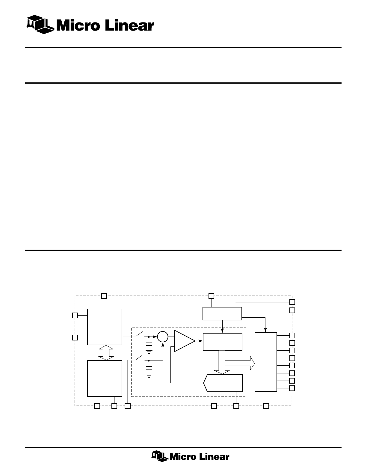
GENERAL DESCRIPTION
The ML2252 and ML2259 combine an 8-bit A/D
converter, 2- or 8-channel analog multiplexer, and a
microprocessor compatible 8-bit parallel interface and
control logic in a single monolithic CMOS device.
Easy interface to microprocessors is provided by the
latched and decoded multiplexer address inputs and a
double buffered three-state data bus. These analog-todigital converters allow the microprocessor to operate
completely asynchronous to the converter clock.
The built in sample and hold function provides the ability
to digitize a 5V, 50kHz sinewave to 8-bit accuracy. The
differential comparator design provides low power supply
sensitivity to DC and AC variations. The voltage reference
can be externally set to any value between ground and
VCC, thus allowing a full conversion over a relatively
small span. All parameters are guaranteed over
temperature with a power supply voltage of 5V ±10%.
The device is suitable for a wide range of applications
from process and machine control to consumer,
automotive, and telecommunication applications.
ML2252 BLOCK DIAGRAM
FEATURES
■ Conversion time (f
■ Total unadjusted error; ±1/2LSB or ±1LSB
■ No missing codes
■ Sample and hold; 390ns acquisition
■ Capable of digitizing a 5V, 50kHz sinewave
■ 2- or 8-channel input multiplexer
■ 0V to 5V analog input range with single 5V
power supply
■ Operates ratiometrically or with up to 5V
voltage reference
■ No zero or full scale adjust required
■ Analog input protection; 25mA per input min
■ Continuous conversion mode
■ Low power dissipation; 15mW max
■ TTL and CMOS compatible digital inputs and outputs
* This Part Is Obsolete
** This Part Is End of Life As Of August 1, 2000
= 1.46MHz); 6.6µs
CLK
CH0
CH1
V
CC
2-CHANNEL
MULTIPLEXER
ADDRESS
LATCH
AND
DECODER
SAMPLE-AND-HOLD FUNCTION
ALE A0 GND +V
+
Σ
8pF
8pF
A/D WITH
+
COMP
–
–
CLOCK
CONTROL
& TIMING
SUCCESSIVE
APPROXIMATION
REGISTER
D/A
CONVERTER
REF
–V
REF
THREE
STATE
OUTPUT
BUFFER
OE
START
EOC
DB0
DB1
DB2
DB3
DB4
DB5
DB6
DB7
1
Page 2
ML2252, ML2259
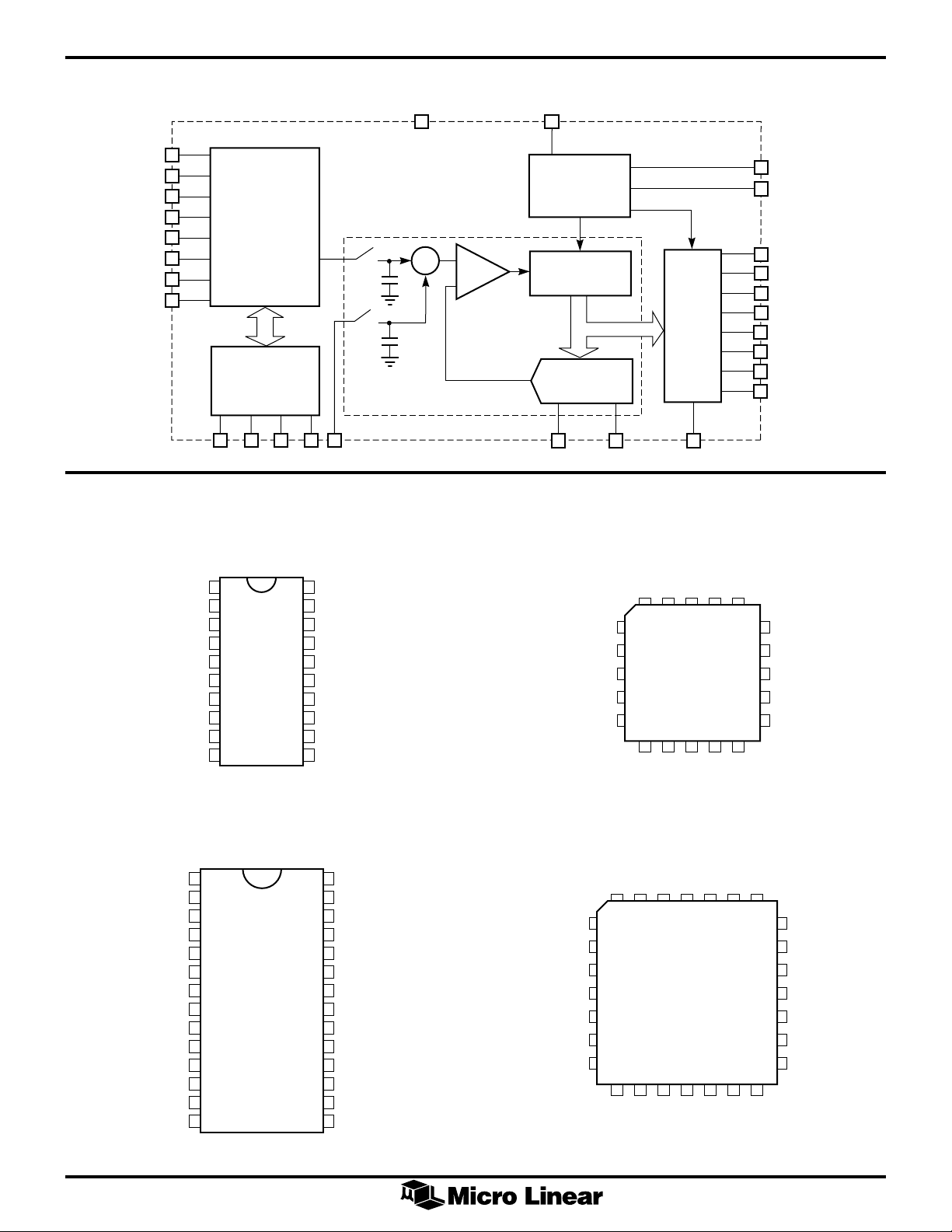
ML2259 BLOCK DIAGRAM
CH0
CH1
CH2
CH3
CH4
8-CHANNEL
MULTIPLEXER
CH5
CH6
CH7
ADDRESS
LATCH
AND
DECODER
ALE A0 A1 A2
PIN CONFIGURATION
ML2252
20-Pin DIP (P20)
V
CC
+
8pF
+
Σ
COMP
–
–
8pF
A/D WITH
SAMPLE-AND-HOLD FUNCTION
GND
CLK
CONTROL
& TIMING
SUCCESSIVE
APPROXIMATION
REGISTER
D/A
CONVERTER
+V
REF
START
EOC
DB0
DB1
DB2
THREE
STATE
OUTPUT
BUFFER
DB3
DB4
DB5
DB6
DB7
–V
REF
OE
ML2252
20-Pin PLCC (Q20)
START
CH3
CH4
CH5
CH6
CH7
START
EOC
DB3
OE
CLK
V
CC
+V
REF
GND
DB1
CH1
1
2
EOC
3
DB3
4
OE
5
CLK
6
V
7
CC
REF
DB1
8
9
10
+V
GND
TOP VIEW
ML2259
28-Pin DIP(P28W)
1
2
3
4
5
6
7
8
9
10
11
12
13
14
TOP VIEW
CH0
20
ADDR0
19
ALE
18
DB7
17
DB6
16
DB5
15
DB4
14
DB0
13
–V
12
11
REF
DB2
+V
DB3
OE
CLK
V
CC
REF
EOL
START
CH1
CH0
3212019
4
5
6
7
8
910111213
GND
DB1
DB2
REF
–V
ADDR0
18
17
16
15
14
DB0
ALE
DB7
DB6
DB5
DB4
TOP VIEW
ML2259
28-Pin PLCC (Q28)
CH2
28
CH1
27
CH0
26
ADDR0
25
ADDR1
24
ADDR2
23
ALE
22
DB7
21
DB6
20
DB5
19
DB4
18
DB0
17
–V
16
15
REF
DB2
CH7
START
EOC
DB3
OE
CLK
V
CC
CH6
CH5
CH4
CH3
432128
5
6
7
8
9
10
11
12 13 14 15 16
REF
DB1
DB2
GND
+V
TOP VIEW
CH2
REF
–V
CH1
27 26
17 18
DB0
CH0
25
24
23
22
21
20
19
DB4
ADDR0
ADDR1
ADDR2
ALE
DB7
DB6
DB5
2
Page 3

ML2252, ML2259
PIN DESCRIPTION
Pin Number
ML2252 ML2259 Name Function
1 CH3 Analog input 3.
2 CH4 Analog input 4.
3 CH5 Analog input 5.
4 CH6 Analog input 6.
5 CH7 Analog input 7.
2 6 START Start of conversion. Active high digital input pulse initiates conversion.
3 7 EOC End of conversion. This output goes low after a START pulse occurs, stays
low for the entire A/D conversion, and goes high after conversion is
completed. Data on DB0–DB7 is valid on rising edge of EOC and stays valid
until next EOC rising edge.
4 8 DB3 Data output 3.
5 9 OE Output enable input. When OE = 0, DB0–DB7 are in high impedance state;
OE = 1, DB0–DB7 are active outputs.
6 10 CLK Clock. Clock input provides timing for A/D converter, S/H, and digital
interface.
711 VCCPositive supply. 5V ±10%.
812 +V
9 13 GND Ground. 0V, all analog and digital inputs or outputs are referenced to this
10 14 DB1 Data output 1.
11 15 DB2 Data output 2.
12 16 –V
13 17 DB0 Data output 0.
14 18 DB4 Data output 4.
15 19 DB5 Data output 5.
16 20 DB6 Data output 6.
17 21 DB7 Data output 7.
18 22 ALE Address latch enable. Input to latch in the digital address (ADDR2-0) on the
23 ADDR2 Address input 2 to multiplexer. Digital input for selecting analog input.
24 ADDR1 Address input 1 to multiplexer. Digital input for selecting analog input.
19 25 ADDR0 Address input 0 to multiplexer. Digital input for selecting analog input.
20 26 CH0 Analog input 0.
1 27 CH1 Analog input 1.
28 CH2 Analog input 2.
REF
REF
Positive reference voltage.
point.
Negative reference voltage.
rising edge of the multiplexer.
3
Page 4
ML2252, ML2259
ABSOLUTE MAXIMUM RATINGS
Absolute maximum ratings are those values beyond which
the device could be permanently damaged. Absolute
maximum ratings are stress ratings only and functional
device operation is not implied.
Supply Voltage, V
.............................................................. 6.5V
CC
Thermal Resistance (qJA)
20-Pin PDIP .....................................................67°C/W
20-Pin PLCC .................................................... 78°C/W
28 Pin PDIP ..................................................... 48°C/W
28-Pin PLCC .................................................... 68°C/W
Logic Inputs ....................................... –0.3V to VCC 0.3V
Analog Inputs ..................................... –0.3V to VCC 0.3V
OPERATING CONDITIONS
Input Current per Pin ............................................±25mA
Storage Temperature ................................–65°C to 150°C
Lead Temperature (Soldering 10 sec.) .................... 260°C
Supply Voltage, V
.............................................. 4.5V to 6.3V
CC
Temperature Range ........................................0°C to 70°C
ELECTRICAL CHARACTERISTICS
Unless otherwise specified, VCC = +V
TA = Operating temperature range (Note 1)
PARAMETER CONDITIONS MIN TYP MAX MIN TYP MAX UNITS
Converter and Multiplexer Characteristics
Total Unadjusted Error V
+V
Voltage Range –V
REF
–V
Voltage Range GND – 0.1 +V
REF
Reference Input Resistance 14 20 35 14 20 28 k ý
Analog Input Range (Note 3) GND – 0.1 VCC + 0.1 GND – 0.1 VCC + 0.1 V
Power Supply Sensitivity DC, VCC = 5V ±10% ±1/32 ±1/4 ±1/32 ±1/4 LSB
I
, Off Channel Leakage On Channel = V
OFF
Current (Note 9) Off Channel = 0V
ION, On Channel Leakage On Channel = 0V, (Note 4) –1 –1 µA
Current (Note 9) Off Channel = V
= V
REF
100mVp-p, 100kHz ±1/16 ±1/16 LSB
Sine on VCC, V
On Channel = 0V, (Note 4) 1 1 µA
Off Channel = V
On Channel = V
Off Channel = 0V
= 5V ±10%, –V
REF
= GND, f
REF
= 1.46MHz,
CLK
ML2252B, ML2259B ML2252C, ML2259C
(Note 2) ±1/2 ±1 LSB
CC,
REF
= 0
IN
(Note 4) –1 –1 µA
CC,
CC
CC
(Note 4) 1 1 µA
CC,
VCC + 0.1 –V
GND – 0.1 +V
REF
REF
VCC + 0.1 V
REF
V
SYMBOL PARAMETER CONDITIONS MIN TYP MAX UNITS
Digital and DC
V
IN(1)
V
IN(0)
I
IN(1)
I
IN(0)
V
OUT(1)
V
OUT(0)
I
OUT
Logical “1” Input Voltage 2.0 V
Logical “0” Input Voltage 0.8 V
Logical “1” Input Current VIN = V
CC
1µA
Logical “0” Input Current VIN = 0V –1 µA
Logical “1” Output Voltage I
Logical “0” Output Voltage I
Three-State Output Current V
= –2mA 4.0 V
OUT
= 2mA 0.4 V
OUT
= 0V –1 µA
OUT
V
OUT
= V
CC
1µA
ICCSupply Current 1.5 3 mA
4
Page 5

ML2252, ML2259
ELECTRICAL CHARACTERISTICS (Continued)
SYMBOL PARAMETER CONDITIONS MIN TYP MAX UNITS
AC and Dynamic Performance Characteristics (Note 5)
t
ACQ
f
CLK
t
C
SNR Signal to Noise Ratio VIN = 51kHz, 5V sine. 47 dB
THD Total Harmonic Distortion VIN = 51kHz, 5V sine. –60 dB
IMD Intermodulation Distortion V
FR Frequency Response V
t
DC
t
EOC
t
WS
t
SS
t
WALE
t
S
t
H
t
H1, H0
t
1H, 0H
C
IN
C
OUT
Note 1: Limits are guaranteed by 100% testing, sampling, or correlation with worst-case test conditions.
Note 2: Total unadjusted error includes offset, full scale, linearity, multiplexer and sample and hold errors.
Note 3: For –V
Note 4: Leakage current is measured with the clock not switching.
Note 5: C
Note 6: A 40% to 60% clock duty cycle range insures proper operation at all clock frequencies. In the case that an available clock has a duty cycle outside of these limits,
Note 7: The conversion start setup time requirement only needs to be satisfied if a conversion must be synchronized to a given clock rising edge. If the setup time is not met,
Sample and Hold Acquisition 1/2 1/f
CLK
Clock Frequency 10 1460 kHz
Conversion Time 8.5 8.5 + 250ns 1/f
= 1.46MHz
f
CLK
(f
SAMPLING
> 150kHz). Noise is sum
CLK
of all nonfundamental components
up to 1/2 of f
= 1.46MHz
f
CLK
(f
SAMPLING
SAMPLING
> 150kHz).
THD is sum 2, 3, 4, 5 harmonics
relative to fundamental
= fA + fB. fA = 49kHz, 2.5V sine. –60 dB
IN
= 47.8kHz, 2.5V sine,
f
B
f
= 1.46MHz
CLK
(f
SAMPLING
– fB), (2fA + fB), (2fA – fB), (fA + 2fB),
(f
A
> 150kHz). IMD is (fA + fB),
(fA – 2fB) relative to fundamental
= 0 to 50kHz. 5V sine relative 0.1 dB
IN
to 1kHz
Clock Duty Cycle (Note 6) 40 60 %
End of Conversion Delay 1/2 1/2 + 250ns 1/f
CLK
Start Pulse Width 50 ns
Start Pulse Setup Time Synchronous only, (Note 7) 40 ns
Address Latch Enable 50 ns
Pulse Width
Address Setup 0 ns
Address Hold 50 ns
Output Enable for DB0–DB7 Figure 1, CL = 50pF 100 ns
Figure 1, CL = 10pF 50 ns
Output Disable for DB0–DB7 Figure 1, CL = 50pF 100 ns
Figure 1, CL = 10pF 50 ns
Capacitance of Logic Input 5 pF
Capacitance of Logic Outputs 10 pF
• VIN (+) the digital output code will be 0000 0000. Two on-chip diodes are tied to each analog input which will forward conduct for analog input voltages
REF
one diode drop below ground or one diode drop greater than the V
cause this input diode to conduct — especially at elevated temperatures, and cause errors for analog inputs near full scale. The spec allow 100mV forward bias of either
diode. This means that as long as the analog V
absolute 0V
= 50pF, timing measured at 50% point.
L
the minimum time the clock is high or the minimum time the clock is low must be at least 40ns. The maximum time the clock can be high or low is 60µs.
start conversion will have an uncertainty of one clock pulse.
to 5VDC input voltage range will therefore require a minimum supply voltage of 4.900VDC over temperature variations, initial tolerance and loading.
DC
or V
does not exceed the supply voltage by more than 100mV, the output code will be correct. To achieve an
IN
REF
supply. Be careful, during testing at low VCC levels (4.5V), as high level analog inputs (5V) can
CC
5
Page 6

ML2252, ML2259
DATA
OUTPUT
DATA
OUTPUT
90%
90%
t
r
10%
t
r
10%
50%
t
0H
50%
t
H0
50%
50%
t
50%
10%
50%
10%
f
90%
t
1H
90%
t
f
90%
t
0H
10%
V
OUTPUT
ENABLE
10k
C
L
OUTPUT
V
CC
10k
C
L
OUTPUT
ENABLE
OUTPUT
CC
GND
V
OH
GND
V
CC
GND
V
CC
V
OL
Figure 1. High Impedance Test Circuits and Waveforms
TYPICAL PERFORMANCE CURVES
1.0
0.75
0.5
LINEARITY ERROR (LSB)
0.25
25°C
0
0.001 0.01 0.1 1.0
CLOCK FREQUENCY (MHz)
VCC = 5V
V
= 5V
REF
Figure 2. Linearity Error vs f
CLK
6
Page 7

TYPICAL PERFORMANCE CURVES (Continued)
ML2252, ML2259
1
VCC = 5V
f
= 1.46MHz
CLK
0.75
0.5
25°C
LINEARITY ERROR (LSB)
0.25
0
01 2 34 5
(VDC)
V
REF
Figure 3. Linearity Error vs V
Voltage
REF
1.0 FUNCTIONAL DESCRIPTION
1.1 MULTIPLEXER ADDRESSING
The ML2252 and ML2259 contain a single ended analog
multiplexer. A particular input channel is selected by
using the address decoder. The relationship between the
address inputs, ADDR0–ADDR2, and the analog input
selected is shown in Table 1. The address inputs are
latched into the decoder on the rising edge of the address
latch signal ALE.
ML2252
SELECTED ADDRESS
ANALOG CHANNEL INPUT
CH0 0
CH1 1
ML2259
SELECTED ADDRESS INPUT
ANALOG CHANNEL ADDR2 ADDR1 ADDR0
CH0 0 0 0
CH1 0 0 1
CH2 0 1 0
CH3 0 1 1
CH4 1 0 0
CH5 1 0 1
CH6 1 1 0
CH7 1 1 1
2
VCC = 5V
V
= 0V
IN
f
= 1.46MHz
CLK
T
= 25°C
1.5
1
OFFSET ERROR (LSB)
0.5
0
01 2 34 5
(VDC)
V
REF
Figure 4. Unadjusted Offset Error vs V
A
REF
Voltage
1.2 A/D CONVERTER
The A/D converter uses successive approximation to
perform the conversion. The converter is composed of the
successive approximation register, the DAC and the
comparator.
The DAC generates the precise levels that determine the
linearity and accuracy of the conversion. The DAC is
composed of a capacitor upper array and a resistor lower
array. The capacitor upper array generates the 4 MSB
decision levels while the series resistor lower array
generates the 4 LSB decision levels. A switch decoder tree
is used to decode the proper level from both arrays.
The capacitor/resistor array offers fast conversion, superior
linearity and accuracy since matching is only required
between 24 = 16 elements (as opposed to 28 = 256
elements in conventional designs). And since the levels are
based on the ratio of capacitors to capacitors and resistors to
resistors, the accuracy and long term stability of the
converter is improved. This also guarantees monotonicity
and no missing codes, as well as eliminating any linearity
temperature or power supply dependence.
The successive approximation register is a digital block
used to store the bit decisions from the conversion.
The comparator design is unique in that it is fully
differential and auto zeroed. The fully differential
architecture provides excellent noise immunity, excellent
power supply rejection, and wide common mode range. The
comparator is auto zeroed at the start of each conversion in
order to remove any DC offset and full scale gain error, thus
improving accuracy and linearity.
Table 1. Multiplexer Address Decoding
7
Page 8

ML2252, ML2259
Another advantage of the capacitor array approach used in
the ML2252 and ML2259 is the inherent sample-and-hold
function. This true S/H allows an accurate conversion to be
done on the input even if the analog signal is not stable.
Linearity and accuracy are maintained for analog signals up
to 1/2 the sampling frequency. As a result, input signals up
to 50kHz can be converted without degradation in linearity
or accuracy.
The sequence of events during a conversion is shown in
figure 5. The rising edge of a START pulse resets the internal
registers and initiates a conversion on the next rising edge
of CLK providing that (tSS) start pulse setup time is satisfied.
If this setup time is not met, start conversion will have an
uncertainty of one clock pulse. The input is then sampled for
the next half CLK period until EOC goes low. EOC goes low
on the falling edge of the next CLK pulse indicating that the
conversion is now beginning. The actual conversion now
takes place for the next eight CLK pulses, one bit for each
CLK pulse. After the conversion is done, the data is updated
on DB0–DB7 and EOC goes high on the rising edge of the
9th CLK pulse, indicating that the conversion has been
completed and data is valid on DB0–DB7. The data will
stay valid on DB0–DB7 until the next conversion updates
the data word on the next rising edge of EOC.
A conversion can be interrupted and restarted at any time
by a new START pulse.
1.3 ANALOG INPUTS AND SAMPLE/HOLD
The ML2252 and ML2259 have a true sample-and-hold
circuit which samples both the selected input and ground
simultaneously. These analog to digital converters can
reject AC common mode signals from DC–50kHz as well
as maintain linearity for signals from DC–50kHz.
The plot in Figure 6 shows a 2048 point FFT of the
ML2259 converting a 50kHz, 0 to 5V, low distortion sine
wave input. The ML2252 and ML2259 sample and
digitize, at their specified accuracy, dynamic input
signals with frequency components up to the Nyquist
frequency (one-half the sampling rate). The output spectra
yields precise measurements of input signal level, harmonic
components, and signal to noise ratio up to the 8-bit level.
The near ideal signal to noise ratio is maintained
independent of increasing analog input frequencies to
50kHz.
The signal at the analog input is sampled during the
interval when the sampling switch is open prior to
conversion start. The sampling window (S/H acquisition
time) is one half CLK period long and occurs one half CLK
period after START goes low. When the sampling switch
closes at the start of the S/H acquisition time, 8pF of
capacitance is thrown onto the analog input. One half
CLK period later, the sampling switch opens, the signal
present at analog input is stored and conversion starts.
Since any error on the analog input at the end of the S/H
acquisition time will cause additional conversion error,
care should be taken to insure adequate settling and
charging time from the source. If more charging or
settling time is needed to reduce these analog input
errors, a longer CLK period can be used.
CLK
START
ALE
ADDR0–ADDR2
EOC
DB0–DB7
OE
Each analog input has dual diodes to the supply rails, and
a minimum of ±25mA (±100mA typically) can be
injected into each analog input without causing latchup.
1/f
CLK
12 4356789
t
SS
t
WS
t
WALE
t
S
t
H
t
EOC
t
C
PREVIOUS DATA DATA
tIH, t
OH
tHI, t
HO
Figure 5. Timing Diagram
8
Page 9

ML2252, ML2259
1.4 REFERENCE
The voltage applied to the +V
and –V
REF
REF
inputs
defines the voltage span of the analog input (the
difference between V
INMAX
and V
) over which the
INMIN
256 possible output codes apply. The devices can be used
in either ratiometric applications or in systems requiring
absolute accuracy. The reference pins must be connected
to a voltage source capable of driving the reference input
resistance, typically 20k.
In a ratiometric system, the analog input voltage is
proportional to the voltage used for the A/D reference.
This voltage is typically the system power supply, so the
+V
pin can be tied to VCC and –V
REF
tied to GND. This
REF
technique relaxes the stability requirements of the system
reference as the analog input and A/D reference move
together maintaining the same output code for a given
input condition.
For absolute accuracy, where the analog input varies
between specific voltage limits, the reference pins can be
biased with a time and temperature stable voltage source.
+V
and –V
REF
GND. In addition, the difference between +V
–V
can be set to small values for conversions over
REF
can be at any voltage between VCC and
REF
REF
and
smaller voltage ranges. Particular care must be taken with
regard to noise pickup, circuit layout ond system error
voltage sources when operating with a reduced span due
to the increased sensitivity converter.
1.5 POWER SUPPLY AND REFERENCE DECOUPLING
A 10µF electrolytic capacitor is recommended to bypass
VCC to GND, using as short a lead length as possible. In
addition, with clock frequencies above 1MHz, a 0.1µF
ceramic disc capacitor should be used to bypass VCC to
GND.
If REF+ and REF– inputs are driven by long lines, they
should be bypassed by 0.1µF ceramic disc capacitors at
the reference input pins (pins 12, 16).
1.6 DYNAMIC PERFORMANCE
Signal-to-Noise Ratio
Signal-to-noise ratio (SNR) is the measured signal to noise
at the output of the converter. The signal is the rms
magnitude of the fundamental. Noise is the rms sum of all
the nonfundamental signals up to half the sampling
frequency. SNR is dependent on the number of
quantization levels used in the digitization process; the
more levels, the smaller the quantization noise. The
theoretical SNR for a sine wave is given by
SNR = (6.02N + 1.76)dB
where N is the number of bits. Thus for ideal 8-bit
converter, SNR = 49.92dB.
Harmonic Distortion
Harmonic distortion is the ratio of the rms sum of
harmonics to the fundamental. Total harmonic distortion
(THD) of the ML2252 and ML2259 are defined as
0
–10
–20
–30
–40
–50
–60
–70
MAGNITUDE (dB)
–80
–90
–100
–110
VVVV
+++
()
log
22324
20
252
V
1
12
/
where V1 is the rms amplitude of the fundamental and V2,
V3, V4, V5 are the rms amplitudes of the individual
harmonics.
37.5 75
FREQUENCY (kHz)
Figure 6. Output Spectrum
9
Page 10

ML2252, ML2259
Intermodulation Distortion
With inputs consisting of sine waves at two frequencies,
fA and fB, any active device with nonlinearities will
create distortion products, of order (m + n), at sum and
difference frequencies of mfA + nfB, where m, n = 0, 1, 2,
3,... . Intermodulation terms are those for which m or n is
not equal to zero. The (IMD) intermodulation distortion
specification includes the second order terms (fA + fB) and
(fA – fB) and the third order terms (2fA + fB), (2fA – fB),
(fA + 2fB) and (fA – 2fB) only.
1.7 DIGITAL INTERFACE
The analog inputs are selected by the digital addresses,
ADDR0–ADDR2, and latched on the rising edge of ALE.
This is described in the Multiplexer Addressing section.
A conversion is initiated by the rising edge of a START
pulse. As long as this pulse is high, the internal logic is
reset.
The sampling interval starts with the following CLK rising
edge after a START falling edge and ends on the falling
edge of CLK. The conversion starts and EOC goes low. The
sampling clock is at least one half CLK period wide. Each
bit conversion in the successive approximation process
takes 1 CLK period. On the rising edge of the ninth CLK
pulse, the digital output of the conversion is updated on
the outputs DB0–DB7 and EOC goes high indicating the
conversion is done and data on DB0–DB7 is valid.
The signal OE drives the data bus, DB0–DB7, into the
high impedance state when held low. This allows the
ML2252 and ML2259 to be tied directly to a µP system
bus without any latches or buffers.
1.7.1 Restart During Conversion
If the A/D is restarted (start goes low and returns high)
during a convesion, the converter is reset and a new
conversion is started. The output data latch is not updated
if the conversion in process is not allowed to be
completed. EOC will remain low and the output data
latch is not updated.
1.7.2 Continuous Conversions
In the free-running, continuous conversion mode, the start
input is tied to the (figure 7) EOC output. An initialization
pulse, following power-up, of mementarily forcing a logic
high level is required to guarantee operation.
V
CC
START
ML2252
ML2259
EOC
START
One feature of the ML2252 and ML2259 is that the data is
double buffered. This means that the outputs DB0–DB7
will stay valid until updated at the end of the next
conversion and will not become invalid when the next
conversion starts. This facilitates interfacing with external
logic of µP.
2.0 TYPICAL APPLICATIONS
+
–
–15V
15V
DC
DC
600Ω
ANALOG
IN
ML2252
ML2259
GND
V
CC
V
CC
+
10µF
XDR
Figure 7. Continuous Conversion Mode
4k
20k
–
1k
24k
1k
ZERO ADJ
3k
ADJ
+
FS
0.85V
–
+
0.15V
CC
CC
+V
REF
ML2252
ML2259
CH
–V
REF
VCC (5VDC)
V
CC
+
10µF
10
Figure 8. Protecting the Input
Figure 9. Operating with Ratiometric Transducers 15% of
VCC - V
- 85% of V
XDR
CC
Page 11

PHYSICAL DIMENSIONS inches (millimeters)
Package: P20
20-Pin PDIP
1.010 - 1.035
(25.65 - 26.29)
20
ML2252, ML2259
0.060 MIN
(1.52 MIN)
(4 PLACES)
0.170 MAX
(4.32 MAX)
0.125 MIN
(3.18 MIN)
PIN 1 ID
1
0.055 - 0.065
(1.40 - 1.65)
0.016 - 0.022
(0.40 - 0.56)
0.385 - 0.395
(9.78 - 10.03)
0.350 - 0.356
(8.89 - 9.04)
1
0.100 BSC
(2.54 BSC)
SEATING PLANE
Package: Q20
20-Pin PLCC
0.240 - 0.260
(6.09 - 6.61)
0.015 MIN
(0.38 MIN)
0.042 - 0.056
0.295 - 0.325
(7.49 - 8.26)
0º - 15º
(1.07 - 1.42)
0.008 - 0.012
(0.20 - 0.31)
0.025 - 0.045
(0.63 - 1.14)
(RADIUS)
0.042 - 0.048
(1.07 - 1.22)
PIN 1 ID
6
0.050 BSC
(1.27 BSC)
0.026 - 0.032
(0.66 - 0.81)
0.013 - 0.021
(0.33 - 0.53)
11
SEATING PLANE
0.350 - 0.356
16
(8.89 - 9.04)
0.165 - 0.180
(4.19 - 4.57)
0.385 - 0.395
(9.78 - 10.03)
0.146 - 0.156
(3.71 - 3.96)
0.009 - 0.011
(0.23 - 0.28)
0.100 - 0.110
(2.54 - 2.79)
0.200 BSC
(5.08 BSC)
0.290 - 0.330
(7.36 - 8.38)
11
Page 12

ML2252, ML2259
PHYSICAL DIMENSIONS inches (millimeters) (Continued)
Package: P28W
28-Pin Wide PDIP
1.440 - 1.460
(36.57 - 37.09)
28
0.070 MIN
(1.77 MIN)
(4 PLACES)
0.190 MAX
(4.83 MAX)
0.125 MIN
(3.18 MIN)
PIN 1 ID
1
0.485 - 0.495
(12.32 - 12.57)
0.450 - 0.456
(11.43 - 11.58)
1
0.050 - 0.065
(1.27 - 1.65)
0.016 - 0.022
(0.40 - 0.56)
Package: Q28
0.100 BSC
(2.54 BSC)
28-Pin PLCC
0.530 - 0.550
(13.46 - 13.97)
SEATING PLANE
0.042 - 0.056
(1.07 - 1.42)
0.015 MIN
(0.38 MIN)
0º - 15º
0.595 - 0.625
(15.11 - 15.88)
0.008 - 0.012
(0.20 - 0.31)
0.025 - 0.045
(0.63 - 1.14)
(RADIUS)
12
0.042 - 0.048
(1.07 - 1.22)
8
0.050 BSC
(1.27 BSC)
0.026 - 0.032
(0.66 - 0.81)
0.013 - 0.021
(0.33 - 0.53)
PIN 1 ID
15
SEATING PLANE
0.450 - 0.456
22
(11.43 - 11.58)
0.165 - 0.180
(4.06 - 4.57)
0.485 - 0.495
(12.32 - 12.57)
0.148 - 0.156
(3.76 - 3.96)
0.009 - 0.011
(0.23 - 0.28)
0.099 - 0.110
(2.51 - 2.79)
0.300 BSC
(7.62 BSC)
0.390 - 0.430
(9.90 - 10.92)
Page 13

ORDERING INFORMATION
TOTAL TEMPERATURE
PART NUMBER UNADJUSTED ERROR RANGE PACKAGE
Two Analog Inputs, 20-Pin Package
ML2252BCP (OBS) ±1/2 LSB 0°C to 70°C Molded DIP (P20)
ML2252BCQ (OBS) 0°C to 70°C Molded PLCC (Q20)
ML2252CCP (OBS)
ML2252CCQ (OBS) 0°C to 70°C Molded PLCC (Q20)
Eight Analog Inputs, 28-Pin Package
ML2259BCP (EOL) ±1/2 LSB 0°C to 70°C Molded DIP (Q28)
ML2259BCQ (OBS) 0°C to 70°C Molded PLCC (Q28)
ML2259CCP (OBS)
ML2259CCQ (OBS) 0°C to 70°C Molded PLCC (Q28)
±1 LSB
±1 LSB
ML2252, ML2259
0°C to 70°C Molded DIP (P20)
0°C to 70°C Molded DIP (P28W)
© Micro Linear 1997 is a registered trademark of Micro Linear Corporation
Products described in this document may be covered by one or more of the following patents, U.S.: 4,897,611; 4,964,026; 5,027,116; 5,281,862; 5,283,483; 5,418,502; 5,508,570; 5,510,727; 5,523,940; 5,546,017;
5,559,470; 5,565,761; 5,592,128; 5,594,376; Japan: 2598946; 2619299. Other patents are pending.
Micro Linear reserves the right to make changes to any product herein to improve reliability, function or
design. Micro Linear does not assume any liability arising out of the application or use of any product
described herein, neither does it convey any license under its patent right nor the rights of others. The
circuits contained in this data sheet are offered as possible applications only. Micro Linear makes no
warranties or representations as to whether the illustrated circuits infringe any intellectual property rights of
others, and will accept no responsibility or liability for use of any application herein. The customer is urged
to consult with appropriate legal counsel before deciding on a particular application.
2092 Concourse Drive
San Jose, CA 95131
Tel: 408/433-5200
Fax: 408/432-0295
DS2252_59-01
13
 Loading...