

Page 1
www.fairchildsemi.com
ML2036
Serial Input Programmable Sine Wave Generator
with Digital Gain Control
Features
• Programmable output frequency – DC to 50kHz
• Low gain error and total harmonic distortion
• 3-wire SPI compatible serial microprocessor interface
with double buffered data latch
• Fully integrated solution – no external components
required
• Frequency resolution of 1.5Hz (±0.75Hz) with a 12MHz
clock input
• Onboard 3 to 12MHz crystal oscillator
• Clock outputs of 1/2 or 1/8 of the input clock frequency
• Synchronous or asynchronous data loading capability
• Compatible with ML2004 logarithmic gain/attenuator
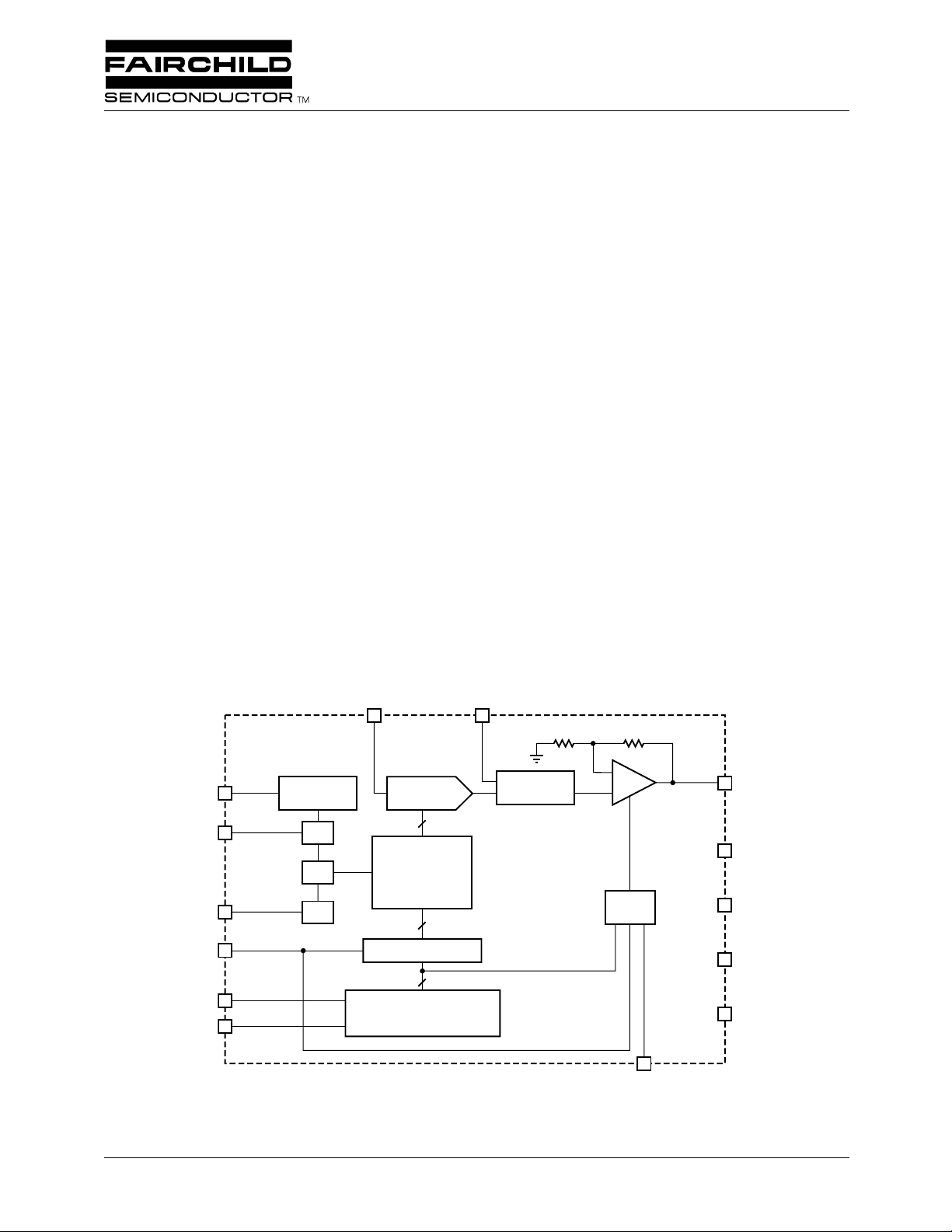
Block Diagram
(Pin configuration shown for 14-Pin PDIP Version)
9
V
REF
General Description
The ML2036 is a monolithic sine wave generator whose
output is programmable from DC to 50kHz. No external
components are required. The frequency of the sinewave
output is derived from either an external crystal or clock
input, providing a stable and accurate frequency reference.
The frequency is programmed by a 16-bit serial data word.
The ML2036 provides for a V
or ±V
/2. Also included with the ML2036 is an inhibit
REF
function which allows the sinewave output to be held at zero
volts after completing the last half cycle of the sine wave in
progress. Two digital clock outputs are provided to drive
other devices with one half or one eighth of the input clock
frequency.
The ML2036 is intended for telecommunications and
modem applications that need low cost and accurate generation of precise test tones, call progress tones, and signaling
tones.
13
GAIN
5kΩ 5kΩ
amplitude of either ±V
OUT
REF
CLK IN
14
CLK OUT 1
3
CLK OUT 2
4
LATI
7
SCK
5
SID
3
CRYSTAL
OSCILLATOR
÷2
÷2
÷2
8-BIT
DAC
8
PHASE
ACCUMULATOR
& 512 POINT
SINE LOOK-UP
TABLE
16
16-BIT DATA LATCH
16
16-BIT SHIFT REGISTER
SMOOTHING
FILTER
-
+
ZERO
DETECT
2
V
OUT
10
V
CC
8
AGND
11
DGND
12
V
SS
1
-INH
P
DN
REV. 1.0.2 7/26/01
Page 2
ML2036 PRODUCT SPECIFICATION
Pin Configuration
1
2
3
4
5
6
7
8
ML2036
TOP VIEW
16
15
14
13
12
11
10
CLK IN
GAIN
NC
DGND
AGND
V
OUT
V
REF
9
V
CC
PDN-INH
CLK OUT 1
CLK OUT 2
Pin Description
ML2036
14-Pin PDIP (P14)
V
SS
SCK
SID
LATI
1
2
3
4
5
6
7
TOP VIEW
14
13
12
11
10
9
8
CLK IN
GAIN
DGND
AGND
V
OUT
V
REF
V
CC
V
PDN-INH
CLK OUT 1
CLK OUT 2
SCK
LATI
(Pin Number in Paranthesis is for SOIC Version)
16-Pin Wide SOIC (S16W)
NC
SS
SID
PIN NAME FUNCTION
1 (2) V
2 (3) P
DN
3 (4) CLK
OUT 1
4 (5) CLK
OUT 2
Negative supply (-5V).
SS
-INH Three level input which controls the inhibit and power down modes. Current source pull-up
to V
.
CC
Digital clock output from the internal clock generator that can drive other devices at f
1
= f
CLK IN
/2.
Digital clock output from the internal clock generator that can drive other devices at f
2
= f
CLK IN
/8.
CLK OUT
CLK OUT
5 (6) SCK Serial clock. Digital input which clocks in serial data on its rising edges.
6 (7) SID Serial input data which programs the frequency of V
OUT
.
7 (8) LATI Digital input which latches serial data into the internal data latch on falling edges.
8 (9) V
9 (10) V
10 (11) V
REF
OUT
Positive supply (5V).
CC
Reference input. The voltage on this pin determines the peak-to-peak swing of V
can be tied to V
CC
.
Analog output.
OUT
. V
11 (12) AGND Analog ground. All analog inputs and outputs are referenced to this point.
12 (13) DGND Digital ground. All digital inputs and outputs are referenced to this point.
13 (15) GAIN Sets V
peak amplitude to V
OUT
REF
or V
/2. Current source pull-down to DGND.
REF
14 (16) CLK IN Clock input. The internal clock can be generated by tying a 3 to 12MHz crystal from this pin
to DGND, or by applying a digital clock signal directly to the pin.
REF
2
REV. 1.0.2 7/26/01
Page 3
PRODUCT SPECIFICATION ML2036
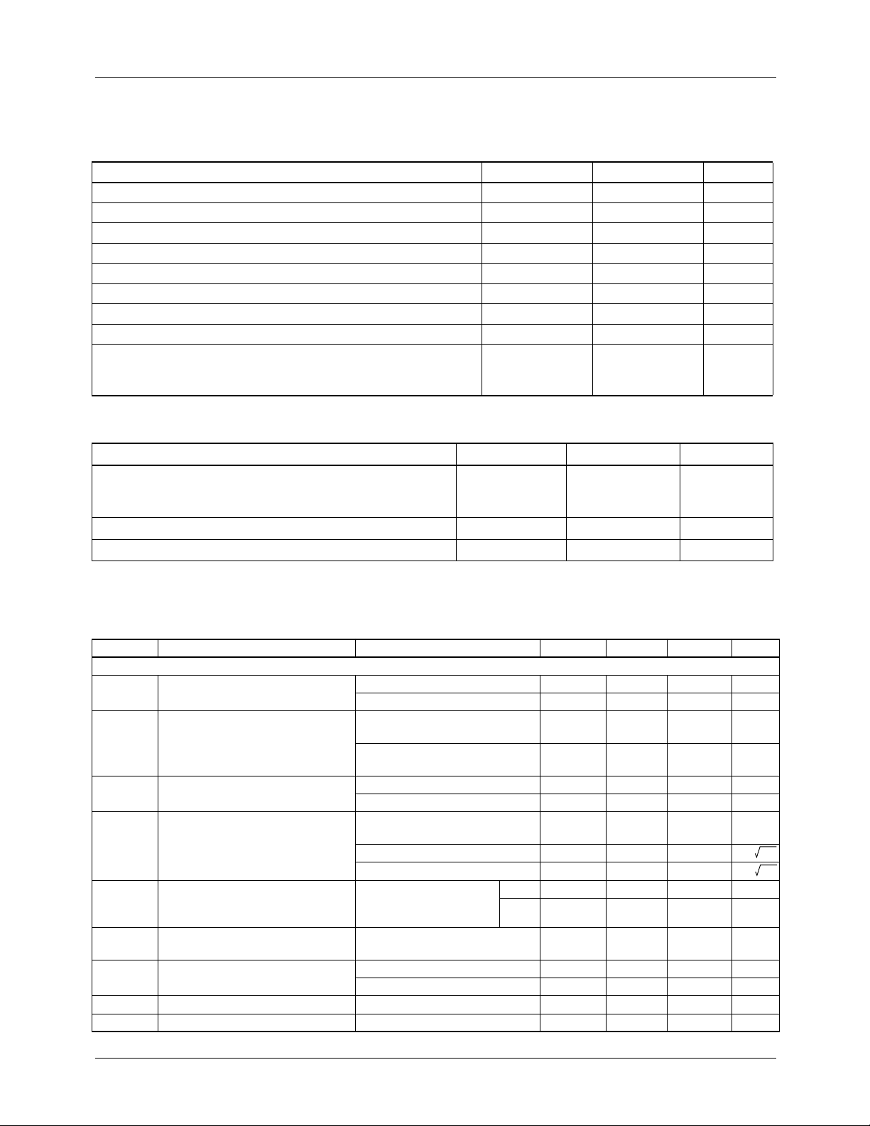
Absolute Maximum Ratings
Absolute maximum ratings are those values beyond which the device could be permanently damaged. Absolute maximum
ratings are stress ratings only and functional device operation is not implied.
Parameter Min. Max. Units
V
CC
V
SS
V
OUT
V
- 0.3 V
SS
Voltage on any other pin GND - 0.3 V
6.5 V
-6.5 V
+ 0.3 V
CC
+ 0.3 V
CC
Input Current ±25 mA
Junction Temperature 150 °C
Storage Temperature Range –65 150 °C
Lead Temperature (Soldering, 10 sec) 260 °C
Thermal Resistance ( θ
14-Pin PDIP
16-Pin Wide SOIC
)
JA
88
105
°C/W
°C/W
Operating Conditions
Parameter Min. Max. Units
Temperature Range
ML2036CX
ML2036IX
V
Range 4.5 5.5 V
CC
V
Range -4.5 -5.5 V
SS
0
-40
70
85
°C
°C
Electrical Characteristics
Unless otherwise specified, V
C
= 100pF, R
L
= 1k Ω , T
L
Symbol Parameter Conditions Min. Typ. Max. Units
Output
HD Harmonic Distortion (Note 2)
(2nd and 3rd Harmonic)
SND Signal to Noise + Distortion
(Note 2)
V
GN
Gain Error (Note 2) 20Hz < f
ICN Idle Channel Noise Power Down Mode, Cmsg
PSRR Power Supply Rejection Ratio 200mV
V
V
V
OS
P-P
Offset Voltage (Note 3) ±(2.5+
OUT
Peak-to-Peak Output Voltage
(Note 2)
V
Swing GAIN = V
OUT
R
REF
Reference Input Resistance 1 6 M Ω
= 4.5V to 5.5V, V
CC
= Operating Temperature Range (Note 1)
A
= -4.5V to -5.5V, V
SS
20Hz to 5kHz -45 dB
5kHz to 50kHz -40 dB
200Hz to 3.4kHz,
f
BW = 200Hz to 4kHz
OUT
20Hz to 50kHz,
BW = 20 Hz to 150kHz
f
OUT
OUT
5kHz < f
OUT
Weighted
Power Down Mode, 1kHz 50 nV/ Hz
Inhibit Mode, 1kHz 500 nV/ Hz
, 0 - 10kHz
P-P
Sine, Measured on
V
OUT
GAIN = V
CC
GAIN = DGND ±V
CC
= 2.5V to V
REF
, CLK IN = 12.352MHz,
CC
-45 dB
-40 dB
< 5kHz ±0.15 dB
< 50kHz ±0.3 dB
-20 0 dBrnc
V
CC
V
SS
±V
REF
REF
V
+1.5 V
SS
-40 dB
-40 dB
V
)/100
P-P
/2 V
-1.5 V
CC
V
V
REV. 1.0.2 7/26/01
3
Page 4
≤
ML2036 PRODUCT SPECIFICATION
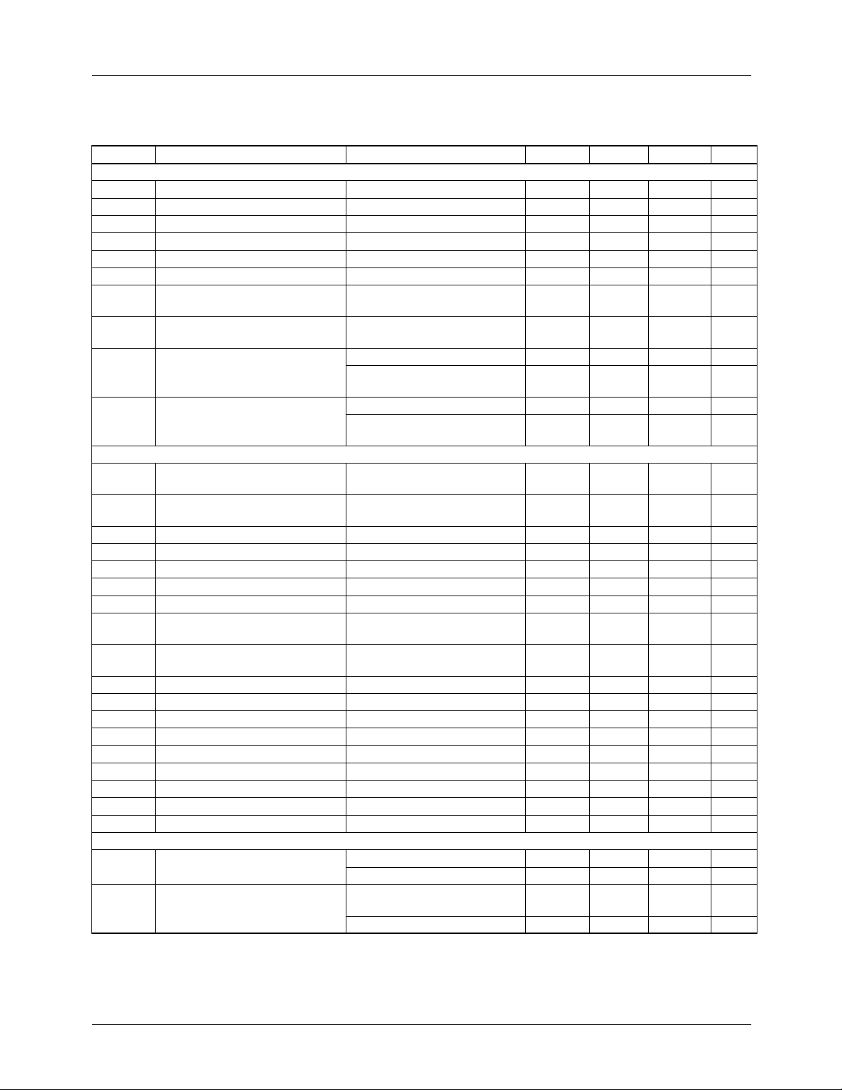
Electrical Characteristics (continued)
Unless otherwise specified, VCC = 4.5V to 5.5V, VSS = -4.5V to -5.5V, V
CL = 100pF, RL = 1kΩ, TA = Operating Temperature Range (Note 1)
Symbol Parameter Conditions Min. Typ. Max. Units
Oscillator
V
CLK CLK IN Input Low Voltage 1.5 V
IL
V
CLK CLK IN Input High Voltage 3.5 V
IH
I
CLK CLK IN Input Low Current -250 µA
IL
I
CLK CLK IN Input High Current 250 µA
IH
C
CLK CLK IN Input Capacitance 12 pF
IN
t
CKI
CLK IN On/Off Period t
CLK OUT 1/CLK IN Frequency
= t
= 10ns, 2.5V Midpoint 30 ns
R
F
See Figure 2 0.49 0.51
Ratio
CLK OUT 2/CLK IN Frequency
See Figure 2 0.122 0.128
Ratio
t
1R
, t
CLK OUT 1, CLK OUT 2 Rise
2R
Time
C
= 40pF, 10% to 90% 20 ns
L
C
= 100pF, 0.8V to 2.0V
L
Transition
, t
t
1F
CLK OUT 1, CLK OUT 2 Fall
2F
Time
C
= 40pF, 90% to 10% 20 ns
L
C
= 100pF, 2.0V to 0.8V
L
Transition
Logic
V
IL
Input Low Voltage (LATI, SCK,
SID, GAIN)
V
IH
Input High Voltage (LATI, SCK,
SID, GAIN)
V
I1
V
I2
V
I3
I
-P
IL
I
-GAIN GAIN Input High Current GAIN = V
IH
I
IL
Input Low Voltage - P
Inhibit Stage Voltage - P
Input High Voltage - P
P
DN
-INH Input Low Current P
DN
Input Low Current (LATI, SCK,
-INH -0.5 0.8 V
DN
-INH V
DN
-INH 2.0 V
DN
-INH = 0V -70 -20 -5 µA
DN
CC
VIN = 0V -1 µA
SID, GAIN)
I
IH
Input High Current (LATI, SCK,
VIN = V
CC
SID, GAIN)
C
V
OL
V
OH
t
SCK
t
DS
t
DH
t
LPW
t
LH
t
LS
IN
Input Capacitance 5 pF
Output Low Voltage IOL = -2mA 0.4 V
Output High Voltage IOH = 2mA 4.0 V
Serial Clock On/Off Period 100 ns
SID Data Setup Time 50 ns
SID Data Hold Time 50 ns
LATI Pulse Width 50 ns
LATI Hold Time 50 ns
LATI Setup Time 50 ns
Supply
I
CC
VCC Current No Load, VCC = V
No Load, Power Down Mode 2 mA
I
SS
VSS Current No Load, VCC = V
5.5V, V
= -5.5V
SS
No Load, Power Down Mode -100 µA
Notes:
1. Limits are guaranteed by 100% testing, sampling, or correlation with worst case test conditions.
2. Maximum peak-to-peak voltage for the output sine wave is: V
the maximum output voltage swing is 2.5V
3. Offset voltage is a function of the peak-to-peak output voltage. For example, if V
P-P
.
OUT(P-P)
= 2.5V to VCC, CLK IN = 12.352MHz,
REF
20 ns
20 ns
0.8 V
2.0 V
+ 0.5 V
SS
5 20 70 µA
1µA
= 5.5V 5.5 mA
REF
=
REF
(125kV x Hz)/f
OUT
OUT(P-P)
. For example, at 50kHz,
= 2.5V, V
-3.5 mA
= ±50mV max.
OS
4
REV. 1.0.2 7/26/01
Page 5

PRODUCT SPECIFICATION ML2036
t
CKItCKI
CLK IN
t
t
SCK
SCK
SCK
t
DStDH
SID
t
t
LS
LH
LATI
t
LPW
Figure 1. Serial Interface Timing.
f
CLKIN
CLK
IN
t
1R
t
1F
CLK
OUT
1
f
CLK
1
2
f
CLK
CLK
OUT
2
t
2F
f
PARAMETERS REFERRED TO 1.4V MIDPOINT
CLK
t
2R
Figure 2. Digital Clock Output Timing
100
75
50
25
0
-25
INPUT CURRENT (µA)
-50
-75
-100
01
INPUT VOLTAGE (V)
2
3
54
Figure 3. CLK IN Input Current vs. Input Voltage.
REV. 1.0.2 7/26/01 5
Page 6

ML2036 PRODUCT SPECIFICATION
PHASE ACCUMULATOR
CLK
IN
OSCILLATOR
BINARY
CRYSTAL
÷4
SID
LATI
A16A
A20A
f
REF
LEAST
SIGNIFICANT
(12 BITS)
PHASE SAMPLES
(7 BITS)
16-BIT
SHIFT REGISTER
(16 BITS)
• • •
16-BIT
DATA LATCH
(16 BITS)
• • •
21-BIT
ADDER
• • •
21-BIT
LATCH
•••
• • •
(7 BITS)
B0–B
0
–
–
15
SUM (21 BITS)
Q
0
•••
QUADRANT
COMPLEMENTER
• • •
20
Q
20
SIGN BIT
QUADRANT
BIT
INPUT TO
QUADRANT
COMPLEMENTOR
INPUT TO
SIGN
BIT
ROM
T =
f
1
REF
READ-ONLY
MEMORY
f
REF
DIGITAL-TO-ANALOG
X 7)
(128
• • •
(7 BITS)
SIGN
COMPLEMENTOR
• • •
(7 BITS)
OUTPUT
LATCH
• • •
(7BITS)
8-BIT
CONVERTER
LOW-PASS
FILTER
SINEWAVE
OUTPUT
SIGN
BIT
SIGN
BIT
INPUT TO SIGN
COMPLEMENTOR
INPUT TO
OUTPUT LATCH
INPUT TO D/A
CONVERTER
Figure 4. Detailed Block Diagram of the ML2036
PICTORIAL
PRESENTATION
OF DIGITAL DATA
INPUT TO
LOW-PASS
FILTER
(ANALOG
SIGNAL)
OUTPUT OF
LOW-PASS
FILTER
(ANALOG
SIGNAL)
6 REV. 1.0.2 7/26/01
Page 7

PRODUCT SPECIFICATION ML2036
Functional Description
The ML2036 is composed of a programmable frequency
generator, a sine wave generator, a crystal oscillator, and
a serial digital interface. The ML2036 frequency and sine
wave generator functional block diagram is shown in
Figure 4.
Programmable Frequency Generator
The programmable frequency generator produces a digital
output whose frequency is determined by a 16-bit digital
word.
The frequency generator is composed of a phase accumulator which is clocked at f
data latch is added to the phase accumulator every 4 cycles
of CLK IN. The frequency of the analog output is equal to
the rate at which the accumulator overflows and is given by
the equation:
f
XD15 D0–()
f
OUT
CLKIN
--------------------------------------------------------------=
23
2
The frequency resolution and the minimum frequency are
the same and is given by the following equation:
f
MIN
CLKIN
-----------------=
2
23
∆f
/4. The value stored in the
CLK IN
DEC
(1)
(2)
The ML2036 has a V
input that can be tied to VCC or
REF
generated from an external voltage. With the GAIN input
equal to a logic “1”, the sine wave peak-to-peak voltage is
equal to ±V
peak voltage is ±V
; with the GAIN equal to a logic “0”, the
REF
/2. However, the overall output volt-
REF
age swing is limited to no closer than 1.5V to either rail.
This means that to avoid clipping, V
can only be tied to
REF
VCC when GAIN is a logic “0”. The sinewave output is
referenced to AGND.
The analog section is designed to operate over a range from
DC to 50kHz. Due to slew rate limitations, the peak-to-peak
output voltage must be limited to V
Hz)/f
to 2.5V
. For example, an output at 50kHz must be limited
OUT
. V
P-P
can drive a 1kΩ, 100pF load and swing
OUT
OUT(P-P)
≤ (125kV x
to within 1.5V of VCC and VSS, provided the slew rate
limitations mentioned above are not exceeded.
The output offset voltage, VOS, is a function of the peak-topeak output voltage and is specified as:
2.5 V
+
V
OS MAX()
For example, if V
V
OS MAX()
±=
OUT(P-P)
± 50mV±==
OUT P P–()
--------------------------------------------
100
= 2.5V:
2.5 2.5+
-----------------------
100
(3)
When f
= 12.352MHz, ∆f
CLK IN
= 1.5Hz (±0.75Hz).
MIN
Lower frequencies are obtained by using a lower input clock
frequency.
Due to the phase quantization nature of the frequency generator, spurious tones can be present in the output range of
–55dB relative to fundamental. The energy from these tones
is included in the signal to noise + distortion specification.
The frequency of these tones can be very close to the fundamental. Therefore, it is not practical to filter them out.
Sinewave Generator
The sinewave generator is composed of a sine look-up table,
a DAC, and an output smoothing filter. The sine look-up
table is addressed by the phase accumulator. The DAC is
driven by the output of the look-up table and generates a
staircase representation of a sine wave.
The output filter smoothes the analog output by removing the
high frequency sampling components. The resultant voltage
on V
distortion components at least 45dB below the fundamental.
is a sinusoid with the second and third harmonic
OUT
SCK
SID
LATI
Crystal Oscillator
The crystal oscillator generates an accurate reference clock
for the programmable frequency generator. The internal
clock can be generated with a crystal or external clock.
If a crystal is used, it must be placed between CLK IN and
DGND of the ML2036. An on-chip crystal oscillator will
then generate the internal clock. No other external capacitors
or components are required. The crystal should be a parallelresonant type with a frequency between 3MHz to 12.4MHz.
It should be placed physically as close as possible to the
CLK IN and DGND.
An external clock can drive CLK IN directly if desired. The
frequency of this clock can be anywhere between 0 and
12MHz.
1514131211109876543210
Figure 5. Serial Interface Timing.
REV. 1.0.2 7/26/01 7
Page 8

ML2036 PRODUCT SPECIFICATION
The crystal must have the following characteristics:
1. Parallel resonant type
2. Frequency: 3MHz to 12.4MHz
3. Maximum equivalent series resistance of 15Ω at a drive
levels of 1µW to 200µW, and 30Ω at drive levels of
10nW to 1µW
4. Typical load capacitance: 18pF
5. Maximum case capacitance: 7pF
The frequency of oscillation will be a function of the crystal
parameters and PC board capacitance. Crystals that meet
these requirements at 12.352000MHz are M-tron 3709-010
12.352 for 0°C to 70°C and 3709-020 12.352 for -40°C to
85°C operation.
The ML2036 has two clock outputs that can be used to drive
other external devices. The CLK OUT 1 output is a buffered
output from the oscillator divided by 2. The CLK OUT 2
output is a buffered output from the oscillator divided by 8.
Serial Digital Interface
The digital interface consists of a shift register and data
latch. The serial 16-bit data word on SID is clocked into a
16-bit shift register on rising edges of the serial shift clock,
SCK. The LSB should be shifted in first and the MSB last as
shown in Figure 4. The data that has been shifted into the
shift register is loaded into a 16-bit data latch on the falling
edge of LATI. To insure that true data is loaded into the data
latch from the shift register, LATI falling edge should occur
when SCK is low, as shown in figure 1. LATI should be low
while shifting data into the shift register to avoid inadvertently entering the power down mode. Note that all data is
entered and latched on the edges, not levels, of SCK and
LATI.
Inhibit and Power Down Modes
The ML2036 has an inhibit mode and a power down mode
which are controlled by the three-level P
described in Table 1. If a logic “1”, (V
–INH input as
DN
) is applied to the
I3
PDN–INH pin, the power down mode is entered by entering
all zeros in the shift register and applying a logic “1” to LATI
and holding it high. A zero data detect circuit detects when
all bits in the shift register are zeros. In this state, the power
consumption is reduced to 11.5mW max, and V
OUT
goes to
0V as shown in Figure 6 and appears as 10kΩ to AGND.
CLK IN can be left active or removed during power down
mode. Also, the ML2036 can be placed in the power down
mode by applying a logic “0” to the P
–INH pin, regard-
DN
less of the contents of the shift register and the state of LATI.
If VSS to VSS + 0.5V (VI2) is applied to the PDN–INH pin,
the inhibit mode is entered by shifting all zeros into the shift
register and applying a logic “1” to the LATI pin. Once the
inhibit mode is entered V
will complete the last half
OUT
cycle of the sinewave and then be held at approximately
VOS, such that no voltage step occurs, as shown in Figure 6.
Power Supplies
The analog circuits in ML2036 are powered from VCC to
VSS and are referenced to AGND. The digital circuits in the
device are powered from VCC to DGND. It is recommended
that AGND and DGND be connected together close to the
device, and have a good connection back to the power
source.
It is recommended that the power supplies to the device
should be bypassed by placing decoupling capacitors from
VCC to AGND and VSS to AGND as physically close to the
device as possible.
8 REV. 1.0.2 7/26/01
Page 9

PRODUCT SPECIFICATION ML2036
Table 1. Three Level PDN-INH Functions.
PDN-INH
MODE
(1)
P
DN
PDN-INH
PIN
VI1, Logic “0” XX V
DATA IN
SHIFT REG. LATI SINE WAVE OUTPUT
= 0V
OUT
(10kΩ to AGND)
Inhibit VI2, Inhibit State
Voltage, VSS to
VSS + 0.5V
(1)
P
DN
VI3, Logic “1” All 0’s Logic “1” V
All 0’s Logic “1” V
goes to approximately VOS at the
OUT
next VOS crossing
(See Figure 6)
= 0V
OUT
(10kΩ to AGND)
Note:
1. In the power down mode, the oscillator, CLK OUT 1 and CLK OUT 2, shift register, and data latch are all functional.
V
0V
0 V
SCK
SID
LATI
OS
V
V
OS
0123456789101112131415
X
V
PEAK
256
V
PEAK
256
FOR f
, FOR f
+ V
OUT
PEAK
>
| =
|V
X
|V
| ≤
X
OUT
f
CLK
2048
SIN
f
CLK
≤
2048
8 π f
OUT
f
CLK
POWER DOWN MODE
INHIBIT MODE
π
+
512
Figure 6. Power Down Mode Waveforms.
REV. 1.0.2 7/26/01 9
Page 10

PRODUCT SPECIFICATION ML2036
Typical Applications
RECEIVE
LINE
INTERFACE
TRANSMIT
LINE
INTERFACE
TONE
DETECTOR
ML2003
ML2004
ATTENUATION
/GAIN
ML2003
ML2004
ATTENUATION
/GAIN
µP
ML2021
LINE
EQUALIZER
ML2036
TONE
GENERATOR
Figure 7. 4-Wire Termination Equipment.
5V
LOOPBACK
RELAY
ML2036
V
GAIN
CC
0.1µF
GND
V
OUT
0.1µF
V
V
SS
REF
2.5V
REF
–5V
Figure 8. Sine Wave Generator with ± 2.5V
P-P
.
REV. 1.0.2 7/26/01 10
Page 11

PRODUCT SPECIFICATION ML2036
Mechanical Dimensions Inches (Millimeters)
Package: P14
14-Pin PDIP
0.740 - 0.760
(18.79 - 19.31)
14
0.070 MIN
(1.77 MIN)
(4 PLACES)
0.170 MAX
(4.32 MAX)
16
0.125 MIN
(3.18 MIN)
(10.16 - 10.52)
PIN 1 ID
1
0.050 - 0.065
0.400 - 0.414
(1.27 - 1.65)
0.016 - 0.022
(0.40 - 0.56)
0.240 - 0.260
(6.09 - 6.61)
0.100 BSC
(2.54 BSC)
SEATING PLANE
Package: S16W
16-Pin Wide SOIC
0.015 MIN
(0.38 MIN)
0.295 - 0.325
(7.49 - 8.25)
0º - 15º
0.008 - 0.012
(0.20 - 0.31)
0.024 - 0.034
(0.61 - 0.86)
(4 PLACES)
0.090 - 0.094
(2.28 - 2.39)
1
PIN 1 ID
0.050 BSC
(1.27 BSC)
0.012 - 0.020
(0.30 - 0.51)
0.291 - 0.301
(7.39 - 7.65)
0.095 - 0.107
(2.41 - 2.72)
SEATING PLANE
0.398 - 0.412
(10.11 - 10.47)
0.005 - 0.013
(0.13 - 0.33)
0º - 8º
0.022 - 0.042
(0.56 - 1.07)
0.009 - 0.013
(0.22 - 0.33)
REV. 1.0.2 7/26/01 11
Page 12

ML2036 PRODUCT SPECIFICATION
Ordering Information
Part Number Temperature Range Package
ML2036CP
ML2036CS
ML2036IP -40°C to 85°C 14-Pin PDIP (P14)
0°C to 70°C
0°C to 70°C
14-Pin PDIP (P14)
16-Pin Wide SOIC (S16W)
DISCLAIMER
FAIRCHILD SEMICONDUCTOR RESERVES THE RIGHT TO MAKE CHANGES WITHOUT FURTHER NOTICE TO
ANY PRODUCTS HEREIN TO IMPROVE RELIABILITY, FUNCTION OR DESIGN. FAIRCHILD DOES NOT ASSUME
ANY LIABILITY ARISING OUT OF THE APPLICATION OR USE OF ANY PRODUCT OR CIRCUIT DESCRIBED HEREIN;
NEITHER DOES IT CONVEY ANY LICENSE UNDER ITS PATENT RIGHTS, NOR THE RIGHTS OF OTHERS.
LIFE SUPPORT POLICY
FAIRCHILD’S PRODUCTS ARE NOT AUTHORIZED FOR USE AS CRITICAL COMPONENTS IN LIFE SUPPORT DEVICES
OR SYSTEMS WITHOUT THE EXPRESS WRITTEN APPROVAL OF THE PRESIDENT OF FAIRCHILD SEMICONDUCTOR
CORPORATION. As used herein:
1. Life support devices or systems are devices or systems
which, (a) are intended for surgical implant into the body,
or (b) support or sustain life, and (c) whose failure to
perform when properly used in accordance with
instructions for use provided in the labeling, can be
reasonably expected to result in a significant injury of the
user.
www.fairchildsemi.com
2. A critical component in any component of a life support
device or system whose failure to perform can be
reasonably expected to cause the failure of the life support
device or system, or to affect its safety or effectiveness.
7/26/01 0.0m 003
© 2001 Fairchild Semiconductor Corporation
Stock#DS30002008
 Loading...