

Page 1
查询ML2035供应商
Serial Input Programmable Sine Wave Generator
February 1997
ML2035
GENERAL DESCRIPTION
The ML2035 is a monolithic sinewave generator whose
output is programmable from DC to 25kHz. No external
components are required. The frequency of the sinewave
output is derived from either an external crystal or clock
input, providing a stable and accurate frequency
reference. The frequency is programmed by a 16-bit serial
data word. The ML2035 has a V
The ML2035 is intended for telecommunications and
modem applications that need low cost and accurate
generation of precise test tones, call progress tones, and
signaling tones.
amplitude of ±VCC/2.
OUT
FEATURES
■ Programmable output frequency - DC to 25kHz
■ Low gain error and total harmonic distortion
■ 3-wire SPI compatible serial microprocessor interface
with double buffered data latch
■ Fully integrated solution - no external components
required
■ Frequency resolution of 1.5Hz (±0.75Hz) with a
12MHz clock input
■ Onboard 3 to 12MHz crystal oscillator
■ Synchronous or asynchronous data loading capability
■ Compatible with ML2031 and ML2032 tone detectors
and ML2004 logarithmic gain/attenuator
BLOCK DIAGRAM
CLK IN
8
LATI
4
SCK
2
SID
3
CRYSTAL
OSCILLATOR
÷4
8-BIT
DAC
8
PHASE
ACCUMULATOR
& 512 POINT
SINE LOOK-UP
TABLE
16
16-BIT DATA LATCH
16
16-BIT SHIFT REGISTER
5kΩ 5kΩ
SMOOTHING
FILTER
-
+
ZERO
DETECT
V
OUT
V
CC
GND
V
6
5
7
SS
1
1
Page 2

ML2035
PIN CONFIGURATION
ML2035
8-Pin PDIP (P08)
V
SS
SCK
SID
LATI
PIN DESCRIPTION
PIN NAME FUNCTION
1V
SS
2 SCK Serial clock. Digital input which
3 SID Serial input data which programs the
4 LATI Digital input which latches serial data
Negative supply (-5V).
clocks in serial data on its rising
edges.
frequency of V
OUT
.
into the internal data latch on falling
edges.
1
2
3
4
TOP VIEW
8
CLK IN
7
GND
6
V
OUT
5
V
CC
PIN NAME FUNCTION
5V
6V
CC
OUT
Positive supply (5V).
Analog output. V
OUT
swing is ±VCC/2.
7 GND Ground. All inputs and outputs are
referenced to this point.
8 CLK IN Clock input. The internal clock can be
generated by tying a 3 to 12MHz
crystal from this pin to GND, or
applying a digital clock signal directly
to the pin.
2
Page 3
ABSOLUTE MAXIMUM RATINGS
ML2035
Absolute maximum ratings are those values beyond which
the device could be permanently damaged. Absolute
Lead Temperature (Soldering, 10 sec) ...................... 260ºC
Thermal Resistance (qJA) .................................... 110ºC/W
maximum ratings are stress ratings only and functional
device operation is not implied.
OPERATING CONDITIONS
V
.............................................................................................. 6.5V
CC
V
............................................................................................. -6.5V
SS
V
.................................................... V
OUT
- 0.3V to VCC + 0.3V
SS
Voltage on any other pin ........ GND - 0.3V to VCC + 0.3V
Input Current ........................................................±25mA
Junction Temperature .............................................. 150ºC
Temperature Range
ML2035CP ................................................. 0ºC to 70ºC
ML2035IP ............................................... -40ºC to 85ºC
VCC Range ...................................................4.5V to 5.5V
VSS Range ................................................. -4.5V to -5.5V
Storage Temperature Range...................... –65ºC to 150ºC
ELECTRICAL CHARACTERISTICS
Unless otherwise specified, VCC = 4.5V to 5.5V, VSS = -4.5V to -5.5V, CLK IN = 12.352MHz, CL = 100pF, RL = 1kW,
TA = Operating Temperature Range (Note 1)
SYMBOL PARAMETER CONDITIONS MIN TYP MAX UNITS
OUTPUT
HD Harmonic Distortion 20Hz to 5kHz -45 dB
(2nd and 3rd Harmonic) 5kHz to 25kHz -40 dB
SND Signal to Noise + Distortion 200Hz to 3.4kHz, -45 dB
f
BW = 20Hz to 4kHz
OUT
20Hz to 25kHz, -40 dB
f
BW = 20 Hz to 75kHz
OUT
V
ICN Idle Channel Noise Power Down Mode, Cmsg Weighted -20 0 dBrnc
Gain Error 20Hz < f
GN
5kHz < f
< 5kHz ±0.15 dB
OUT
< 25kHz ±0.3 dB
OUT
Power Down Mode, 1kHz 50 nV/ÖHz
PSRR Power Supply Rejection Ratio 200mV
Sine, Measured on V
V
V
OSCILLATOR
VIL CLK CLK IN Input Low Voltage 1.5 V
VIH CLK CLK IN Input High Voltage 3.5 V
IIL CLK CLK IN Input Low Current -250 µA
IIH CLK CLK IN Input High Current 250 µA
CIN CLK CLK IN Input Capacitance 12 pF
t
CKI
LOGIC (LATI, SID, SCK)
V
V
I
I
V
OS
P-P
IL
IH
IL
IH
Offset Voltage ±75 mV
OUT
Peak-to-Peak Output Voltage ±VCC/2 V
CLK IN On/Off Period tR = tF = 10ns, 2.5V Midpoint 30 ns
Input Low Voltage 0.8 V
Input High Voltage 2.0 V
Input Low Current VIN = 0V -1 µA
Input High Current VIN = V
, 0 - 10kHz V
P-P
OUT
CC
CC
V
SS
-40 dB
-40 dB
1µA
3
Page 4
ML2035
ELECTRICAL CHARACTERISTICS (Continued)
SYMBOL PARAMETER CONDITIONS MIN TYP MAX UNITS
LOGIC (Continued)
V
V
t
t
t
LPW
t
OH
SCK
t
DS
DH
LH
t
Output Low Voltage IOL = -2mA 0.4 V
OL
Output High Voltage IOH = 2mA 4.0 V
Serial Clock On/Off Period 100 ns
SID Data Setup Time 50 ns
SID Data Hold Time 50 ns
LATI Pulse Width 50 ns
LATI Hold Time 50 ns
LATI Setup Time 50 ns
LS
SUPPLY
I
CC
VCC Current No Load, VCC = 5.5V 5.5 mA
No Load, Power Down Mode 2 mA
I
VSS Current No Load, VCC = 5.5V, VSS = -5.5V -3.5 mA
SS
No Load, Power Down Mode -100 µA
Note 1: Limits are guaranteed by 100% testing, sampling, or correlation with worst case test conditions.
CLK IN
SCK
SID
LATI
100
t
t
DStDH
CKItCKI
t
t
SCK
t
LS
SCK
t
LPW
t
LH
75
50
25
0
-25
INPUT CURRENT (µA)
-50
-75
-100
01
2
INPUT VOLTAGE (V)
3
54
Figure 1. Serial Interface Timing. Figure 2. CLK IN Input Current vs. Input Voltage.
4
Page 5

FUNCTIONAL DESCRIPTION
ML2035
The ML2035 is composed of a programmable frequency
generator, a sine wave generator, a crystal oscillator, and a
serial digital interface. The ML2035 frequency and sine
wave generator functional block diagram is shown in
Figure 3.
PROGRAMMABLE FREQUENCY GENERATOR
The programmable frequency generator produces a digital
output whose frequency is determined by a 16-bit digital
word.
The frequency generator is composed of a phase
accumulator which is clocked at f
CLK IN
/4. The value
stored in the data latch is added to the phase accumulator
every 4 cycles of CLK IN. The frequency of the analog
output is equal to the rate at which the accumulator
overflows and is given by the equation:
f
OUT
CLKIN DEC
=
23
2
(1)
f D15- D0)
×(
The frequency resolution and the minimum frequency are
the same and is given by the following equation:
f
∆f
When f
MIN
CLKIN
=
23
2
= 12.352MHz, Df
CLK IN
= 1.5Hz (±0.75Hz).
MIN
(2)
Lower frequencies are obtained by using a lower input
clock frequency.
Due to the phase quantization nature of the frequency
generator, spurious tones can be present in the output
range of –55dB relative to fundamental. The energy from
these tones is included in the signal to noise + distortion
specification. The frequency of these tones can be very
close to the fundamental. Therefore, it is not practical to
filter them out.
SINEWAVE GENERATOR
The sinewave generator is composed of a sine look-up
table, a DAC, and an output smoothing filter. The sine
look-up table is addressed by the phase accumulator. The
DAC is driven by the output of the look-up table and
generates a staircase representation of a sine wave.
The output filter smoothes the analog output by removing
the high frequency sampling components. The resultant
voltage on V
is a sinusoid with the second and third
OUT
harmonic distortion components at least 45dB below the
fundamental.
The ML2035 provides a peak sinewave voltage of ±VCC/2,
referenced to GND.
must be limited to 25kHz for VCC = 5V. V
can drive a
OUT
1kW, 100pF loads, provided the slew rate limitations
mentioned above are not exceeded.
The output offset voltage, VOS, is a function of the peak-topeak output voltage and is specified as:
(3)
For example, if V
OUT(P-P)
= 2.5V:
CRYSTAL OSCILLATOR
The crystal oscillator generates an accurate reference
clock for the programmable frequency generator. The
internal clock can be generated with a crystal or external
clock.
If a crystal is used, it must be placed between CLK IN and
GND of the ML2035. An on-chip crystal oscillator will
then generate the internal clock. No other external
capacitors or components are required. The crystal should
be a parallel-resonant type with a frequency between
3MHz to 12.4MHz. It should be placed physically as close
as possible to the CLK IN and GND.
An external clock can drive CLK IN directly if desired. The
frequency of this clock can be anywhere between 0 and
12MHz.
The crystal must have the following characteristics:
1. Parallel resonant type
2. Frequency: 3MHz to 12.4MHz
3. Maximum equivalent series resistance of 15W at a drive
levels of 1µW to 200µW, and 30W at drive levels of
10nW to 1µW
4. Typical load capacitance: 18pF
5. Maximum case capacitance: 7pF
The frequency of oscillation will be a function of the
crystal parameters and PC board capacitance. Crystals that
meet these requirements at 12.352000MHz are M-tron
3709-010 12.352 for 0ºC to 70ºC and 3709-020 12.352
for -40ºC to 85ºC operation.
The analog section is designed to operate over a range
from DC to 25kHz. Due to slew rate limitations, the peakto-peak output voltage must be limited to V
(125kV x Hz)/f
. Since the ML2035 peak-to-peak output
OUT
OUT(P-P)
£
voltage is equal to VCC, the maximum output frequency
5
Page 6
ML2035
CLK IN
BINARY
PHASE ACCUMULATOR
CRYSTAL
OSCILLATOR
÷4
SID
LATI
f
REF
LEAST
SIGNIFICANT
(12 BITS)
PHASE SAMPLES
(7 BITS)
16-BIT
SHIFT REGISTER
(16 BITS)
• • •
16-BIT
DATA LATCH
(16 BITS)
• • •
A16A
0
21-BIT
–
–
ADDER
A20A
15
SUM (21 BITS)
• • •
21-BIT
LATCH
Q
0
••••••
QUADRANT
COMPLEMENTER
• • •
(7 BITS)
• • •
B0–B
20
Q
20
SIGN BIT
QUADRANT
BIT
INPUT TO
QUADRANT
COMPLEMENTOR
INPUT TO
SIGN
BIT
ROM
T =
f
1
REF
f
REF
DIGITAL-TO-ANALOG
READ-ONLY
MEMORY
X
7)
(128
• • •
(7 BITS)
SIGN
COMPLEMENTOR
• • •
(7 BITS)
OUTPUT
LATCH
• • •
(7BITS)
8-BIT
CONVERTER
LOW-PASS
FILTER
SINEWAVE
OUTPUT
SIGN
BIT
SIGN
BIT
INPUT TO SIGN
COMPLEMENTOR
INPUT TO
OUTPUT LATCH
INPUT TO D/A
CONVERTER
PICTORIAL
PRESENTATION
OF DIGITAL DATA
INPUT TO
LOW-PASS
FILTER
(ANALOG
SIGNAL)
OUTPUT OF
LOW-PASS
FILTER
(ANALOG
SIGNAL)
Figure 3. Detailed Block Diagram of the ML2035.
6
Page 7

SCK
SID
LATI
Figure 4. Serial Interface Timing.
FUNCTIONAL DESCRIPTION (Continued)
ML2035
1514131211109876543210
SERIAL DIGITAL INTERFACE
The digital interface consists of a shift register and data
latch. The serial 16-bit data word on SID is clocked into a
16-bit shift register on rising edges of the serial shift clock,
SCK. The LSB should be shifted in first and the MSB last as
shown in Figure 4. The data that has been shifted into the
shift register is loaded into a 16-bit data latch on the falling
edge of LATI. To insure that true data is loaded into the
data latch from the shift register, LATI falling edge should
occur when SCK is low, as shown in figure 1. LATI should
be low while shifting data into the shift register to avoid
inadvertently entering the power down mode. Note that all
data is entered and latched on the edges, not levels, of
SCK and LATI.
POWER DOWN MODE
The power down mode of the ML2035 can be selected by
entering all zeros in the shift register and applying a logic
“1” to LATI and holding it high. A zero data detect circuit
detects when all bits in the shift register are zeros. In this
state, the power consumption is reduced to 11.5mW max,
and V
goes to 0V as shown in Figure 5 and appears as
OUT
10kW to ground. The master clock, CLK IN, can be left
active or removed during power down mode.
POWER SUPPLIES
The analog circuits in ML2035 are powered from VCC to
VSS and are referenced to GND. The digital circuits in the
device are powered from VCC to GND.
It is recommended that the power supplies to the device
should be bypassed by placing decoupling capacitors from
VCC to GND and VSS to GND as physically close to the
device as possible.
POWER DOWN MODE
Figure 5. Power Down Mode Waveforms.
0V
SCK
SID
LATI
V
OS
0123456789101112131415
7
Page 8
ML2035
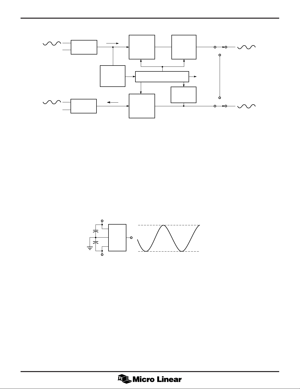
TYPICAL APPLICATIONS
RECEIVE
LINE
INTERFACE
TRANSMIT
LINE
INTERFACE
ML2003
ML2031
ML2032
TONE
DETECTOR
ML2004
ML2008
ML2009
ATTENUATION
/GAIN
µP
ML2003
ML2004
ML2008
ML2009
ATTENUATION
/GAIN
ML2020
ML2021
LINE
EQUALIZER
ML2035
TONE
GENERATOR
Figure 6. 4-Wire Termination Equipment.
LOOPBACK
RELAY
5V
ML2035
V
CC
0.1µF
0.1µF
–5V
GND
V
SS
V
OUT
0 TO 25kHz SINEWAVE
Figure 7. Sine Wave Ratiometric to ±VCC/2.
/2
V
CC
/2
V
CC
8
Page 9

PHYSICAL DIMENSIONS inches (millimeters)
Package: P08
8-Pin PDIP
0.365 - 0.385
(9.27 - 9.77)
0.055 - 0.065
(1.39 - 1.65)
8
ML2035
0.020 MIN
(0.51 MIN)
(4 PLACES)
0.170 MAX
(4.32 MAX)
0.125 MIN
(3.18 MIN)
PIN 1 ID
1
0.100 BSC
(2.54 BSC)
0.016 - 0.020
(0.40 - 0.51)
SEATING PLANE
0.240 - 0.260
(6.09 - 6.60)
0.015 MIN
(0.38 MIN)
0.299 - 0.335
(7.59 - 8.50)
0º - 15º
0.008 - 0.012
(0.20 - 0.31)
ORDERING INFORMATION
PART NUMBER TEMPERATURE RANGE PACKAGE
ML2035CP 0ºC to 70ºC 8-Pin PDIP (P08)
ML2035IP -40ºC to 85ºC 8-Pin PDIP (P08)
© Micro Linear 1997. is a registered trademark of Micro Linear Corporation.
Products described herein may be covered by one or more of the following patents: 4,897,611; 4,964,026; 5,027,116; 5,281,862; 5,283,483; 5,418,502; 5,508,570; 5,510,727; 5,523,940; 5,546,017; 5,559,470;
5,565,761; 5,592,128; 5,594,376. Other patents are pending.
Micro Linear reserves the right to make changes to any product herein to improve reliability, function or
design. Micro Linear does not assume any liability arising out of the application or use of any product
described herein, neither does it convey any license under its patent right nor the rights of others. The
circuits contained in this data sheet are offered as possible applications only. Micro Linear makes no
warranties or representations as to whether the illustrated circuits infringe any intellectual property rights of
others, and will accept no responsibility or liability for use of any application herein. The customer is urged
to consult with appropriate legal counsel before deciding on a particular application.
2092 Concourse Drive
San Jose, CA 95131
Tel: (408) 433-5200
Fax: (408) 432-0295
DS2035-01
9
 Loading...