

Page 1
www.fairchildsemi.com
REV. 1.1.1 3/19/01
Features
• Slope, height, and bandwidth adjustable
• Optimized group delays (500 Hz to 6.4 kHz)
• On chip anti-alias filter
• Bypass mode
• Low supply current 6 mA typical from ±5V supplies
• TTL / CMOS compatible interface
• Double buffered data latch
• Selectable master clock 1.544 or 1.536 MHz
• Synchronous or asynchronous data loading capability
• Compatible with ML2003 and ML2004 logarithmic
gain/attenuator
General Description
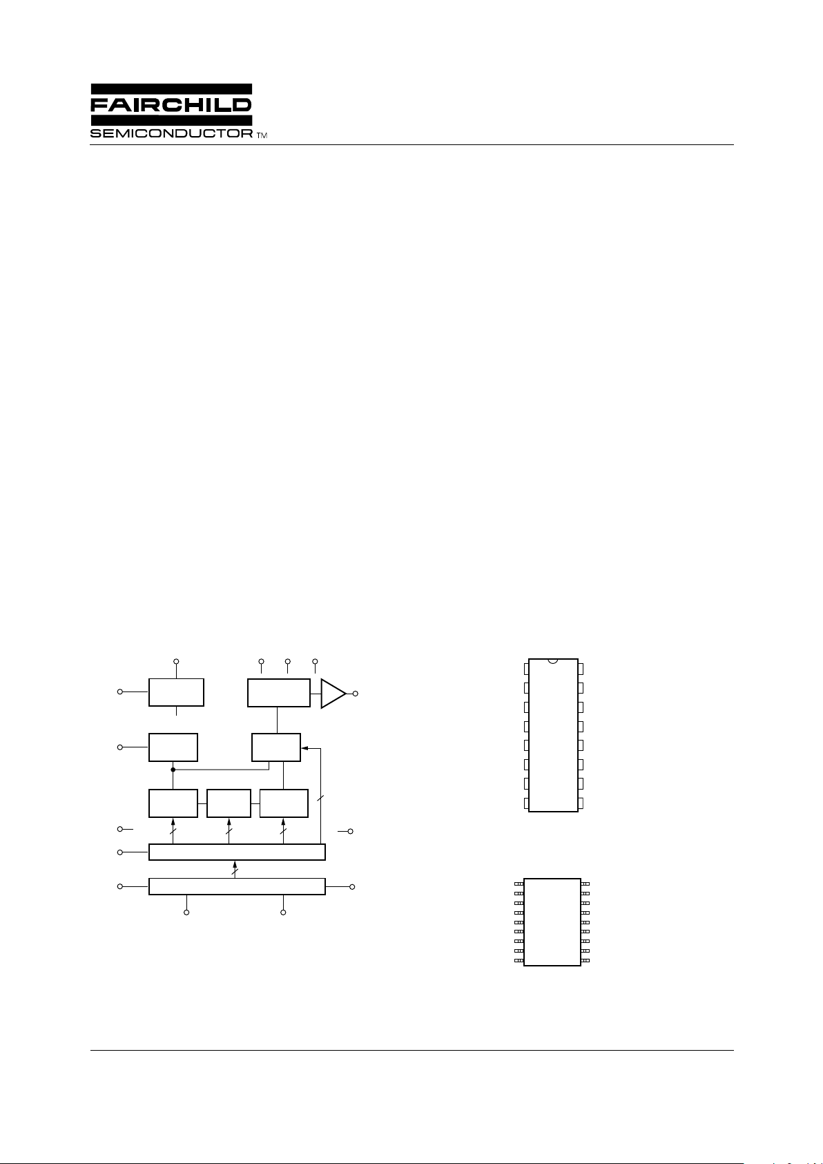
The ML2021 is a monolithic analog line equalizer for telephone applications. The ML2021 consists of a switched
capacitor filter that realizes a family of frequency response
curves optimized for telephone line equalization while minimizing group delay.
The ML2021 consists of a continuous anti-aliasing filter,
three programmable switched capacitor equalization filters,
an output smoothing filter, a 600 Ω driver, and a digital
section for the serial interface.
The equalization filters adjust the slope, height, and bandwidth of the frequency response. The desired frequency
response is programmed by a digital 14-bit serial input data
stream.
Block Diagram Pin Connections
CLKSEL AGND
CLKSEL
SID
NC
LATO
SCK
NC
SOD
CLK
CLKSEL
SID
NC
LATO
SCK
NC
SOD
CLK
V
CC
V
CC
P
DN
P
DN
V
OUT
AGND
AGND
V
IN
V
SS
V
SS
V
IN
V
OUT
LATI
LATI
NC
NC
GND
GND
TOP VIEW
TOP VIEW
1
1
2
3
4
5
6
7
8
9
18
17
16
15
14
13
12
11
10
2
3
4
5
6
7
8
16
15
14
13
12
11
10
9
CLK
CLOCK
GENERATOR
SMOOTHING
FILTER
MUX
ANTIALIAS
LO PASS
SLOPE
SECTION
HEIGHT
SECTION
BANDPASS
SECTION
V
CC
V
IN
P
DN
LATI
SID
V
OUT
GND
SOD
SCK LATO
1
544
14
14-BIT LATCH
14-BIT SHIFT REGISTER
V
SS
ML2021
16-PIN DIP
ML2021
18-PIN SOIC
ML2021
Telephone Line Equalizer
Page 2

ML2021 PRODUCT SPECIFICATION
2
REV. 1.1.1 3/19/01
Pin Description
Absolute Maximum Ratings
1
Operating Conditions
Name Function
CLKSEL Clock select input. This pin selects the frequency of the CLK input. If CLK is 1.536 MHz, set
CLKSEL = 1. If CLK is 1.544 MHz, set CLKSEL = 0. Pin has an internal pullup resistor to V
CC
.
SID
Serial input data. Digital input that contains serial data word which controls the filter frequency
response setting.
LATO
Output latch clock. Digital input which loads the data word back into the shift register from the latch.
SCK
Shift clock. Digital input which shifts the serial data on SID into the shift register on rising edges and
out onto SOD on falling edges.
SOD
Serial output data. Digital output of the shift register.
CLK
Master clock input. Digital input which generates clocks for the switched capacitor filters.
Frequency can be either 1.544 MHz or 1.536 MHz.
GND
Digital ground. 0 volts. All digital inputs and output are referenced to this ground.
LATI
Input latch clock. Digital input which loads data from the shift register into the latch.
V
SS
Negative supply. –5volts ±10%.
V
IN
Analog input.
AGND
Analog ground. 0 volts. Analog input and output are referenced to this ground.
V
OUT
Analog output.
P
DN
Powerdown input. When P
DN
= 1, device is in powerdown mode. When P
ND
= 0, device is in normal
operation. This pin has an internal pulldown resistor to GND.
V
CC
Positive supply. 5 volts ± 10%
Parameter Min. Max. Units
Supply Voltage
V
CC
V
SS
+6.5
-6.5
V
V
AGND with respect to GND ±0.5 V
Analog Input and Output V
SS
–0.3 V
CC
+0.3 V
Digital Input and Outputs GND –0.3 V
CC
+0.3 V
Input Current Per Pin ±25 mA
Power Dissipation 750 mW
Storage Temperature Range -65 +150 °C
Lead Temperature (Soldering, 10 sec) 300 °C
Parameter Min. Max. Units
Temperature Range
2
ML2021CX
ML2021IX
0
-40
70
85
°C
°C
Supply Voltage
V
CC
V
SS
4
-4
6
-6
V
V
Page 3

PRODUCT SPECIFICATION ML2021
REV. 1.1.1 3/19/01
3
Electrical Characteristics
Unless otherwise specified T
A
= T
MIN
to T
MAX
, V
CC
= 5V ± 10%, V
SS
= -5V ± 10%, Data Word: BP
= 1,
Other Bits = 0, C
L
= 100pF, R
L
= 600 Ω , dBm measurements use 600 Ω as reference load, V
IN
= -7dBm,
1kHz sinusoid CLK = 1.544 MHz ±300 Hz and digital time measured at 1.4 V
Symbol Parameter Notes Conditions Min Typ.
3
Max. Units
Analog
SR Response, Slope Section 4 1 kHz response
NL/L
S3 S2 S1 S0
0
0
0
0
0
1
1
1
1
1
1
0
0
0
1
1
0
0
0
0
1
1
0
0
1
0
1
0
0
0
1
0
1
0
1
0
0
1
0
0
1
0
0
1
1
0
0
0
1
0
1
0
0
0
1
1.4 ±0.1
2.6 ±0.2
4.7 ±0.2
7.8 ±0.2
11.4 ±0.25
0 ±0.1
0.4 ±0.1
0.9 ±0.2
1.8 ±0.2
3.7 ±0.2
6.6 ±0.25
dB
dB
dB
dB
dB
dB
dB
dB
dB
dB
dB
Referenced to
0 0000
HR Response, Height
Section
4 3250 Hz response referenced to 1 kHz
response with BP = 1, other bits = 0
NL/L
H3 H2 H1 H0
0
0
0
0
0
0
0
0
0
0
1
1
0
0
0
1
0
1
0
0
1
0
0
1
0
1
0
0
0
1
0 ±0.15
0.5 ±0.2
1.1 ±0.2
2.3 ±0.2
5.7 ±0.3
11.1 ±0.3
dB
dB
dB
dB
dB
dB
BR Response, Bandwidth
Section (Q)
4
NL/L
B3 B2 B1 B0 H3 H2 H1 H0
0
0
0
0
0
0
0
0
0
0
1
1
0
0
0
1
0
1
0
0
1
0
0
1
0
1
0
0
0
1
1
1
1
1
1
1
1
1
1
1
1
1
1
1
1
1
1
1
1
1
1
1
1
1
16.1 ±2.0
14.2 ±1.5
12.6 ±1.5
9.1 ±1.0
3.6 ±0.5
1.2 ±0.35
PK BW Peak Frequency 4 H3 thru H0 = 1 3230 3250 3270 Hz
AG Absolute Gain, Flat
Response
4 0.5 kHz to 4 kHz -0.1 +0.1 +0.3 dB
AGB Absolute Gain, Bypass
Mode
4 0.3 kHz to 4 kHz, BP = 0 -0.1 +0.1 +0.3 dB
ICN Idle Channel Noise 4 V
IN
= 0 3 8 dBrnc
V
IN
= 0, All Data Bits = 1 9 dBrnc
HD Harmonic Distortion 4 V
IN
= 5 dBm, 1 kHz
Measure 2nd, 3rd, harmonic
relative to fundamental
-48 dB
SD Signal to Distortion 4 V
IN
= -12dBm, 1 kHz
C msg weighted
+48 dB
SFN Signal Frequency Noise 5 V
IN
= 0, 4 kHz ≤ frequency ≤ 150 kHz -50 dBm
PSRR Power Supply Rejection 4 200mV
p-p
, 1 kHz sine, V
IN
= 0
on V
CC
on V
SS
-40
-40
dB
dB
Page 4

ML2021 PRODUCT SPECIFICATION
4
REV. 1.1.1 3/19/01
Notes
1. Absolute maximum ratings are limits beyond which the life of the integrated circuit may be impaired. All voltages unless
otherwise specified are measured with respect to ground.
2. 0°C to +70°C and –40°C to +85°C operating temperature range devices are 100% tested with temperature limits guaranteed
by 100% testing, sampling, or by correlation with worst-case test conditions.
3. Typicals are parametric norm at 25°C.
4. Parameter guaranteed and 100% production tested.
5. Parameter guaranteed. Parameters not 100% tested are not in outgoing quality level calculation.
Z
IN
Input Impedance, V
IN
4 100 k Ω
V
OS
Output Offset Voltage 4 V
IN
= 0 ±50 mV
V
INR
Input Voltage Range 4 ±2.0 V
V
OSW
Output Voltage Swing 4 R
L
= 600 Ω
±2.0 V
Digital and DC
V
IL
Digital Input Low Voltage 4 0.8 V
V
IH
Digital Input High Voltage 4 2.0 V
V
OL
Digital Output Low
Voltage
4I
OL
= 2mA 0.4 V
V
OH
Digital Output High
Voltage
4I
OH
= –1mA 4.0 V
I
LCLK
Input Current, CLK SEL 4 V
IN
= 0 5 100 µA
I
LPDN
Input Current, PDN 4 V
IN
= V
CC
-3 -100 µA
I
L
Input Current, All Other
Inputs
4V
IN
= 0 to V
CC
±10 µA
I
CC
V
CC
Supply Current 4 No output load, V
IL
= GND,
V
IH
= V
CC
, V
IN
= 0
10 mA
I
SS
V
SS
Supply Current 4 No output load, V
IL
= GND,
V
IH
= V
CC
, V
IN
= 0
-10 mA
I
CCP
V
CC
Supply Current,
Powerdown Mode
4 No output load, V
IL
= GND,
V
IH
= V
CC
1.2 mA
I
SSP
VSS Supply Current,
Powerdown Mode
4 No output load, V
IL
= GND,
VIH = V
CC
-1.2 mA
AC Characteristics
t
DC
Clock Duty Cycle 5 40 60 %
t
SCK
SCK On/Off Period 4 250 ns
t
S
SID Data Setup Time 4 50 ns
t
H
SID Data Hold Time 4 50 ns
t
D
SOD Data Delay 4 0 125 ns
t
IPW
LATI Pulse Width 4 50 ns
t
OPW
LATO Pulse Width 4 50 ns
tIS, t
OS
LATI, LATO Setup Time 4 50 ns
t
IH
, t
OH
LATI, LATO Hold Time 5 50 ns
t
PLD
SOD Parallel Load Delay 4 0 125 ns
Electrical Characteristics (continued)
Unless otherwise specified TA = T
MIN
to T
MAX
, VCC = 5V ± 10%, VSS = -5V ± 10%, Data Word: BP = 1,
Other Bits = 0, CL = 100pF, RL = 600Ω, dBm measurements use 600Ω as reference load, VIN = -7dBm,
1kHz sinusoid CLK = 1.544 MHz ±300 Hz and digital time measured at 1.4 V
Symbol Parameter Notes Conditions Min Typ.3Max. Units
Page 5

PRODUCT SPECIFICATION ML2021
REV. 1.1.1 3/19/01 5
Figure 1. Serial Timing Diagram
Figure 2. Typical Slope Filter Response—NL/L = 0
B3-B0, H3-H0 = 0000, S3-S0 = 0000 to 1111.
SCK
t
SCK
t
SCK
t
S
t
IS
t
IH
t
OS
t
OH
t
IPW
t
OPW
t
PLD
t
D
t
H
SID
SOD
SCK
LATI
LATO
SOD
TIMING PARAMETERS ARE REFERENCED TO THE 1.4 VOLT MIDPOINT.
12
10.5
9.0
7.5
6.0
4.5
3.0
1.5
0
0 500 1000 1500 2000
FREQUENCY (Hz)
AMPLITUDE (dB)
2500 3000 3500 4000
0000
1111
–1.5
–3.0
0 500 1000 1500 2000
FREQUENCY (Hz)
2500 3000 3500 4000
100
120
80
60
40
20
0
–20
–40
GROUP DELAY—dφ/df(µs)
–60
–80
0100
1000
1111
0010
0001
0000
Page 6

ML2021 PRODUCT SPECIFICATION
6 REV. 1.1.1 3/19/01
Figure 3. Typical Slope Filter Response—NL/L = 1
B3-B0, H3-H0 = 0000, S3-S0 = 0000 to 1111.
Figure 4. Typical Height Filter Response—NL/L = 0
B3-B0, S3-S0 = 0000, H3-H0 = 0000 to 1111.
Figure 5. Typical Bandwidth Filter Response—NL/L = 0
H3-H0 = 1111; S3-S0 = 0000; B3-B0 = 0000 to 1111.
12
10.5
9.0
7.5
6.0
4.5
3.0
1.5
0
0 500 1000 1500 2000
FREQUENCY (Hz)
AMPLITUDE (dB)
2500 3000 3500 4000
0000
1111
–1.5
–20
0
20
40
–40
–60
–80
–100
–120
–140
0 500 1000 1500 2000
FREQUENCY (Hz)
GROUP DELAY – dφ/df (µs)
2500 3000 3500 4000
–160
–3.0
1111
1000
0000
0100
0010
0001
12
10.5
9.0
7.5
6.0
4.5
3.0
1.5
0
0 500 1000 1500 2000
FREQUENCY (Hz)
AMPLITUDE (dB)
2500 3000 3500 4000
–1.5
1000
1200
800
600
400
200
0
0 500 1000 1500 2000
FREQUENCY (Hz)
GROUP DELAY – dφ/df (µs)
2500 3000 3500 4000
–200
–3.0
1111
1111
1000
0100
0010
0001 0000
0000
0010
0001
0100
1000
12
10.5
9.0
7.5
6.0
4.5
3.0
1.5
0
0 500 1000 1500 2000
FREQUENCY (Hz)
AMPLITUDE (dB)
2500 3000 3500 4000
–1.5
1000
1200
800
600
400
200
0
0 500 1000 1500 2000
FREQUENCY (Hz)
GROUP DELAY – dφ/df (µs)
2500 3000 3500 4000
–200
–3.0
1111
0000
0000
0100
1000
1111
0010
0001
Page 7

PRODUCT SPECIFICATION ML2021
REV. 1.1.1 3/19/01 7
Functional Description
The ML2021 consists of a continuous anti-alias filter, three
programmable switched capacitor equalization filters, an
output smoothing filter, an output driver, and a digital section
for the serial interface.
Anti-Alias Filter
The first section is a continuous anti-alias filter. This filter is
needed to prevent aliasing of high frequency signal present
on the input into the passband by the sampling action of the
switched capacitor filters. This section is a continuous second order lowpass filter with a typical 3 dB frequency at 20
kHz and 30 dB of rejection at 124 kHz.
Equalization Filters
The programmable filters implement a family of frequency
response curves intended to compensate for the response of
telephone lines.
This filter is composed of three distinct sections: slope,
height, and bandwidth.
Response of Slope, Height, and Bandwidth
The family of response curves generated by the slope section
are shown in Figures 2 and 3. There are 4 slope select bits,
S3-S0. These bits alter the slope of the highpass response
under 1000Hz, and as a result, the absolute gain above 1000
Hz will be unique for each setting. Table 1 gives typical 1
kHz gain values for all slope settings.
Table 1. Typ. 1kHz Gain for Slope Settings
HT, BW Bits = 0
There is an additional bit, NL/L, that also affects the highpass response of the slope filter. The slope response curves in
Figure 2 are with NL/L = 0. These same response curves are
shown in Figure 3 with NL/L = 1. Notice that the NL/L bit
adds more droop in the highpass response below 2500 Hz.
The family of response curves generated by the height section are shown in Figure 4. There are 4 height select bits,
H3-H0. This section creates a peak in the response at 3250
Hz and this filter controls the amount of peaking. Table 2
gives typical 1 kHz gain values for all height and bandwidth
settings.
Table 2. Typ. 1kHz Gain for HT and BW Settings
Slope Bits = 0
The family of response curves generated by the bandwidth
section is shown in Figure 5. There are 4 bandwidth select
bits, B3-B0. This section causes the response of the 3250 Hz
peak to be widened, and as a result, this filter controls the
bandwidth of the 3250 Hz peaked region.
Transfer Function
The transfer function for the ML2021 is shown below. This
transfer function is valid for magnitude response only. The
actual magnitude response from an individual device may
deviate from the computed response from the transfer function by typically 0–0.2 dB.
s = j × 256000 × tan (πf/128000)
ωo= 20463.77
fc = 128000
b,c : See Table 3. (slope)
Q : See Table 4. (bandwidth)
h : See Table 5. (height)
Slope
Setting
Rel 1kHz Gain (dB)
NL/L = 1 NL/L = 0
0
1
0.0
0.4
REL
1.4
2
3
0.9
1.4
2.6
3.7
4
5
1.8
2.3
4.7
5.5
6
7
2.8
3.4
6.3
7.2
8
9
3.7
4.2
7.8
8.4
10
11
4.6
5.0
9.0
9.5
12
13
5.4
5.8
10.0
10.5
14
15
6.2
6.6
11.0
11.4
Relative 1kHz Gain (dB)
HT Setting
0123456789101112131415
BW Setting
01Rel000000000000000000000000000000
0
230000000000000000000000000000000
0
450000000000000000000000000
0.100.100.1
0.1
0.1
6700000000000000000
0.100.1
0.1
0.1
0.1
0.1
0.1
0.1
0.1
0.2
0.1
0.2
0.1
0.2
8900000000000
0.1
0.1
0.1
0.1
0.1
0.1
0.1
0.1
0.2
0.1
0.2
0.2
0.3
0.2
0.3
0.3
0.4
0.3
0.5
0.4
0.6
10110000000
0.1
0.1
0.1
0.1
0.1
0.1
0.2
0.1
0.2
0.2
0.3
0.3
0.4
0.3
0.4
0.4
0.5
0.5
0.7
0.6
0.8
0.7
0.9
0.8
1.1
121300000.1
0.1
0.1
0.1
0.1
0.2
0.2
0.3
0.2
0.4
0.3
0.5
0.4
0.6
0.5
0.8
0.7
0.9
0.8
1.1
1.0
1.4
1.1
1.6
1.4
1.9
1.6
2.3
141500000.1
0.1
0.1
0.1
0.2
0.2
0.3
0.3
0.4
0.4
0.5
0.5
0.7
0.7
0.8
0.9
1.0
1.1
1.2
1.3
1.5
1.6
1.7
1.8
2.0
2.1
2.4
2.5
Hs()
cs b+()
bs c+()
--------------------
s
2
h ωoQ⁄()s ω
o
2
++[]
s
2
ωoQ⁄()s ω
o
2
++[]
---------------------------------------------------------
×
πffc⁄()sin[]
πffc⁄()
-------------------------------
×=
Page 8

ML2021 PRODUCT SPECIFICATION
8 REV. 1.1.1 3/19/01
Table 3. Slope Response Factors (b,c)
Table 4. Slope Response factors (b,c)
Table 5. Height Response Factors (h)
Group Delay
The difference between the ML2020 and ML2021 is the
elimination of a 60 Hz highpass filter in order to eliminate
positive group delay at low frequency.
The group delay through the ML2021 can be minimized
such that less than 50µs of group delay can be achieved
in both unloaded and cable loaded conditions relative to
1804 Hz in the frequency range of 504 to 3004Hz. Minimum
group delays are dependant upon using the proper
setting for slope, height, and bandwidth for a give equalization requirement.
Smoothing Filter
The equalizer filters are followed by a continuous second
order smoothing filter that removes the high frequency
sample information generated by the action of the switched
capacitor filters. This filter provides a continuous analog
signal at the output, V
OUT
.
Output Buffer
The final stage in the ML2021 is the output buffer. This
amplifier has internal gain of 1 and is capable of driving
600Ω, 100pF loads. Thus, it is suitable for driving telephone
hybrids directly without any external amplifier.
Bypass Mode
The filter sections can be bypassed by setting the bypass data
bit, BP, to 0. Since the switched capacitor filters are bypassed
in this mode, frequency response effects of the switched
capacitor filters are eliminated. Thus, this mode offers very
flat response and low noise over the 300-4000 Hz frequency
range.
Filter Clock
The master clock, CLK, is used to generate the internal
clocks for the switched capacitor filters. The frequency of
CLK can be either 1.544 MHz or 1.536 MHz. However, the
internal clock frequency must be kept at 1.536 MHz to
guarantee accurate frequency response. The CLKSEL pin
enables a bit swallower circuit to keep the internal clock
frequency set to 1.536 MHz. When 1.544 MHz clock is used,
CLKSEL should be set to logic level 0, and one bit out of
every 193 bits is removed (swallowed) to reduce the internal
frequency to 1.536 MHz. When 1.536 MHz clock is used,
CLKSEL should be set to logic level 1, and the internal clock
rate is the same as the external clock rate.
Serial Interface
The architecture of the digital section is shown in the preceding block diagram.
A timing diagram for the serial interface is shown in Figure
6. The serial input data, SID, is loaded into a shift register on
rising edges of the shift clock, SCK. The data word is parallel loaded into a latch when the input latch signal, LATI, is
S3-0bNL/L = 0
b
NL/L = 1
0000
0001
0010
0011
0100
0101
0110
0111
1000
1001
1010
1011
1100
1101
1110
1111
2.371759E +03
1.985920E + 03
1.701779E + 03
1.493571E + 03
1.326721E + 03
1.196668E + 03
1.087277E + 03
9.983588E + 02
9.179889E + 02
8.537864E + 02
7.966049E + 02
7.478074E + 02
7.035099E + 02
6.651771E + 02
6.299477E + 02
5.990361E + 02
1.116280E + 04
9.345141E + 03
8.007156E + 03
7.026999E + 03
6.241681E + 03
5.629636E + 03
5.114881E + 03
4.696487E + 03
4.318339E + 03
4.016273E + 03
3.747249E + 03
3.517676E + 03
3.309279E + 03
3.128945E + 03
2.963214E + 03
2.817797E + 03
S3-0cNL/L = 0
c
NL/L = 1
XXXX 2.371759E + 03 1.116280E + 04
B3-0 Q
0000
0001
0010
0011
0100
0101
0110
0111
1000
1001
1010
1011
1100
1101
1110
1111
17.444906
15.386148
13.652451
11.593677
9.859960
8.017864
6.392453
5.092080
3.900003
3.141338
2.599369
2.165724
1.731965
1.406509
1.352248
1.297981
Code h
0000
0001
0010
0011
0100
0101
0110
0111
1000
1001
1010
1011
1100
1101
1110
1111
1.000000
1.071519
1.148154
1.230269
1.318257
1.445438
1.603245
1.757924
1.949845
2.137962
2.317395
2.540973
2.786121
3.019951
3.311311
3.672823
Page 9

PRODUCT SPECIFICATION ML2021
REV. 1.1.1 3/19/01 9
high. The LATI pulse must occur when SCK is low. A new
data word can be loaded into the shift register without disturbing the existing data word in the latch.
The parallel outputs of the latch control the filter response
curves. The order of the data word bits in the latch is shown
in Figure 7.
Note that bit 0 is the first bit of the data word clocked into the
shift register.
The device has the capability to read out the data word stored
in the latch. This is done by parallel loading the data from
the latch back into the shift register when the latch signal,
LATO, is high. The LATO pulse must occur when SCK is
low. Then, the data word can be shifted out of the register
serially to the output, SOD, on falling edges of the shift
clock, SCK.
The loading and reading of the data word can be done continuously or in bursts. Since the shift register and latch circuitry inside the device is static, there are no minimum
frequency requirements on the clocks or data pulses. However, there is some coupling of the digital signals in the analog section. If this coupling is undesirable, the data can be
clocked in bursts during non critical intervals, or the data rate
can be done at a frequency outside the analog frequency
range.
The clocks used to shift and latch data (SCK, LATI, LATO)
are not related internally to the master clock and can occur
asynchronous to CLK.
Figure 6. Serial Timing
Figure 7. 14-Bit Latch
SCK
012345678910111213
012345
a) LOAD
b) READ
6 7 8 9 10 11 12 13
SID BP H0 H1 H2 H3 B0 B1 B2 B3 S0 S1 S2 S3 NL/L
LATI
LATO
SOD
SCK
SID
LATI
LATO
SOD
BP H0 H1 H2 H3 B0 B1 B2 B3 S0 S1 S2 S3 NL/L
NL/L
NL/L S3 S2 S1
131211109876543210
S0 B3 B2 B1 B0 H3 H2 H1 H0
SLOPE BANDWIDTH HEIGHT BYPASS
FUNCTION
BIT NUMBER
BP
Page 10

ML2021 PRODUCT SPECIFICATION
10 REV. 1.1.1 3/19/01
Powerdown Mode
A powerdown mode can be selected with pin PDN. When
PDN = 1, the device is powered down. In this state, the power
consumption is reduced by removing power from the analog
section and forcing the analog output, V
OUT
, to a high
impedance state. While the device is in power down mode,
the digital section is still functional and the current data word
remains stored in the latch. The master clock, CLK, can
be left active or removed during powerdown mode. When
P
DN
= 0, the device is in normal operation.
Power Supplies
The digital section inside the device is powered between
VCC and GND, or 5 volts. The analog section is powered
between V
CC
and VSS, or ±5 volts. The analog section uses
AGND as the reference point.
GND and AGND are totally isolated inside the device to
minimize coupling from the digital section into the analog
section. Typically this is less than 100 µV. However, ANGD
and GND should be tied together physically near the device
and close to the common power supply ground connection.
The power supply rejection of V
CC
and VSS to the analog
output is greater than –60dB at 1 kHz, typically. If decoupling of the power supplies is still necessary in a system,
VCC and VSS should be decoupled with respect to AGND.
Applications
Figure 8. Typical Serial Interface
Figure 9. Controlling Multiple ML2021 and ML2004 With
Only 3 Digital Lines Using One Long Data Word
ML2004
LOG GAIN/ATTEN
ML2021
EQUALIZER
V
IN
V
OUT
µP
V
IN
SID
SCK
LATI
SID
SCK
LATI
V
OUT
µP
ML2021 OR ML2004
V
IN
V
OUT
SID
SCK
LATI
SOD
ML2021 OR ML2004
V
IN
V
OUT
SID
SCK
LATI
SOD
ML2021 OR ML2004
V
IN
V
OUT
SID
SCK
LATI
SOD
Page 11

ML2021 PRODUCT SPECIFICATION
3/19/01 0.0m 003
Stock#DS300042021
2001 Fairchild Semiconductor Corporation
LIFE SUPPORT POLICY
FAIRCHILD’S PRODUCTS ARE NOT AUTHORIZED FOR USE AS CRITICAL COMPONENTS IN LIFE SUPPORT DEVICES
OR SYSTEMS WITHOUT THE EXPRESS WRITTEN APPROVAL OF THE PRESIDENT OF FAIRCHILD SEMICONDUCTOR
CORPORATION. As used herein:
1. Life support devices or systems are devices or systems
which, (a) are intended for surgical implant into the body,
or (b) support or sustain life, and (c) whose failure to
perform when properly used in accordance with
instructions for use provided in the labeling, can be
reasonably expected to result in a significant injury of the
user.
2. A critical component in any component of a life support
device or system whose failure to perform can be
reasonably expected to cause the failure of the life support
device or system, or to affect its safety or effectiveness.
www.fairchildsemi.com
DISCLAIMER
FAIRCHILD SEMICONDUCTOR RESERVES THE RIGHT TO MAKE CHANGES WITHOUT FURTHER NOTICE TO
ANY PRODUCTS HEREIN TO IMPROVE RELIABILITY, FUNCTION OR DESIGN. FAIRCHILD DOES NOT ASSUME
ANY LIABILITY ARISING OUT OF THE APPLICATION OR USE OF ANY PRODUCT OR CIRCUIT DESCRIBED HEREIN;
NEITHER DOES IT CONVEY ANY LICENSE UNDER ITS PATENT RIGHTS, NOR THE RIGHTS OF OTHERS.
Ordering Information
Part Number Temperature Range Package
ML2021CP 0°C to 70°C Molded DIP (P16)
ML2021CS 0°C to 70°C Molded SOIC (S18)
ML2021IP -40°C to 85°C Molded DIP (P16)
ML2021IS -40°C to 85°C Molded SOIC (S18)
 Loading...