

Page 1
DATASHEET
VIDEO GENLOCK PLL MK9173-01/-15
Description
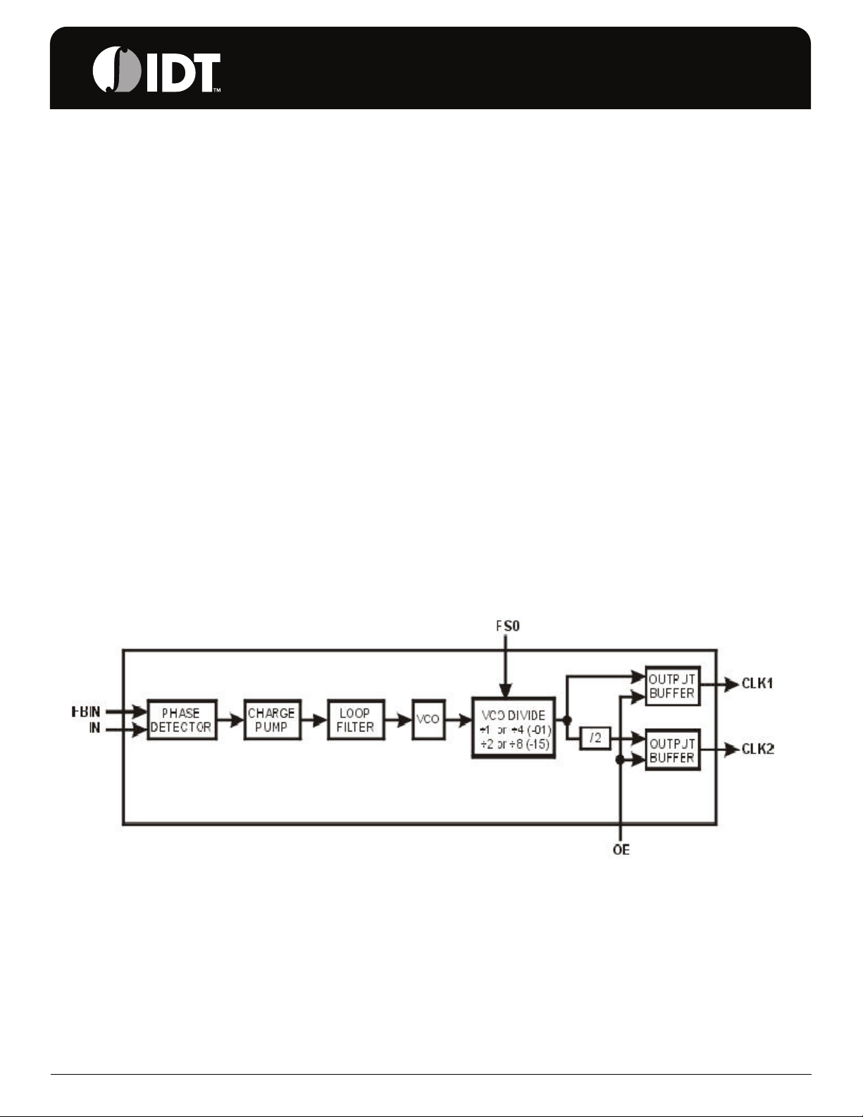
The MK9173-01/-15 provide the analog PLL circuit blocks
to implement a frequency multiplier. Because the device is
configured to use an external divider in the PLL clock
feedback path, a large divider can be used to result in a
large frequency multiplication ratio. This is useful when
using a low frequency input clock to generate a high
frequency output clock. The MK9173-01/-15 contains a
phase detector, charge pump, loop filter, and
voltage-controlled oscillator (VCO). The ICS674-01 can be
used as the external feedback divider.
A common application of the MK9173-01/-15 is the
implementation of a video genlock circuit. Because of this,
the MK9173-01/-15 inputs operate on the negative-going
clock edge.
The MK9173-01/-15 is pin and function compatible to the
AV9173-01/15.
Block Diagram
Features
• Phase-detector/VCO circuit block
• Ideal for genlock system
• Reference clock range 12 kHz to 1 MHz for full output
clock range
• Output clock range of 1.25 to 75 MHz (-01), and 0.625 to
37.5 MHz (-15). See “Allowable Input Frequency to
Output Frequency” table for conditions
• On-chip loop filter
• Single 5 V power supply
• Low power CMOS technology
• 8-pin SOIC package
• For new video genlock applications, please refer to the
ICS673-01, ICS1522 or ICS1523.
IDT™
VIDEO GENLOCK PLL 1
MK9173-01/-15 REV C 12/21/06
Page 2
MK9173-01/-15
VIDEO GENLOCK PLL CLOCK SYNTHESIZER
Pin Assignment
FBIN
IN
GND
FS0
2
3
4
8 pin SOIC
8
CLK21
VDD
7
CLK1
6
5
OE
Pin Descriptions
Pin Number Pin Name Pin Type Pin Description
1 FBIN Input Feedback input.
2 IN Input Input for reference sync pulse.
3 GND Power Ground.
4 FS0 Input Frequency select 0 input.
5 OE Input Output enable.
6 CLK1 Output Clock output 1.
7 VDD Power Power supply (+5 V).
8 CLK2 Output Clock output 2.
Allowable Input Frequency to Output Frequency for MK9173-01 (in MHz)
(MK9173-15 outputs run at exactly half of the MK9173-01 frequencies)
f
for FS = 0 f
OUT
f
(kHz)
IN
12 <
fIN < 14 kHz 44.0 to 75 22.0 to 37.5 11.0 to 18.75 5.5 to 9.375
14 < f
17 < f
30 < f
35 < f
< 17 kHz 30.0 to 75 15.0 to 37.5 7.5 to 18.75 3.75 to 9.375
IN
< 30 kHz 25.0 to 75 12.5 to 37.5 6.25 to 18.75 3.125 to 9.375
IN
< 35 kHz 15.0 to 75 7.5 to 37.5 3.75 to 18.75 1.875 to 9.375
IN
< 1000 kHz 10.0 to 75 5.0 to 37.5 2.5 to 18.75 1.25 to 9.375
IN
CLK1 Output CLK2 Output CLK1 Output CLK2 Output
for FS = 1
OUT
IDT™
VIDEO GENLOCK PLL 2
MK9173-01/-15 REV C 12/21/06
Page 3
MK9173-01/-15
VIDEO GENLOCK PLL CLOCK SYNTHESIZER
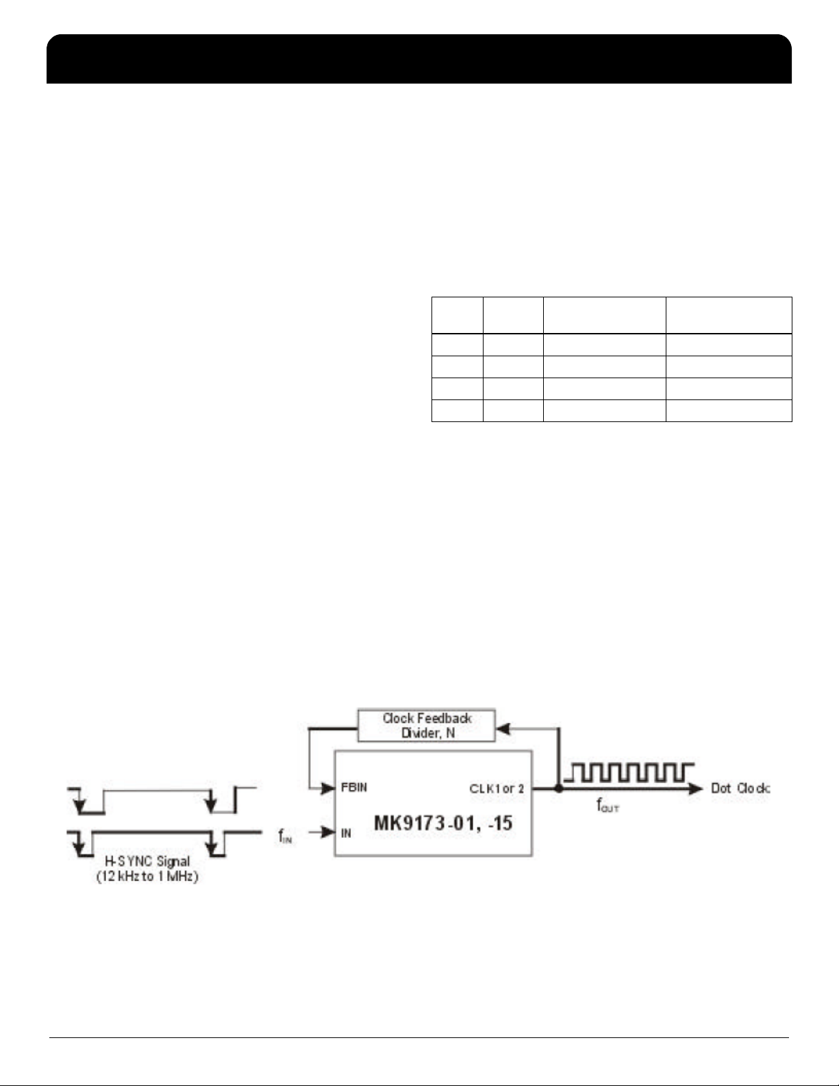
Using the MK9173-01/-15 in Genlock Applications
Most video sources, such as video cameras, are
asynchronous, free-running devices. To digitize video or
synchronize one video source to another free-running
reference video source, a video “genlock” (generator lock)
circuit is required. The MK9173-01/-15 integrate the analog
blocks which make the task much easier.
In the complete video genlock circuit, the primary function of
the MK9173-01/-15 is to provide the analog circuitry
required to generate the video dot clock within a PLL. This
application is illustrated in Figure 1. The input reference
signal for this circuit is the horizontal synchronization
(H-SYNC) signal. If a composite video reference source is
being used, the h-sync pulses must be separated from the
composite signal. A video sync separator circuit, such as the
National Semiconductor LM1881, can be used for this
purpose.
The clock feedback divider shown in Figure 1 is a digital
divider used within the PLL to multiply the reference
frequency. Its divide ratio establishes how many video dot
clock cycles occur per h-sync pulse. For example, if 880
pixel clocks are desired per h-sync pulse, then the divider
ratio is set to 880. Hence, together the h-sync frequency and
external divider ratio establish the dot clock frequency:
The output hook-ups of the MK9173-01/-15 are dictated by
the desired dot clock frequency. The primary consideration
is the internal VCO which operates over a frequency range
of 10 MHz to 75 MHz. Because of the selectable VCO
output divider and the additional divider on output CLK2,
four distinct output frequency ranges can be achieved. The
following Table lists these ranges and the corresponding
device configuration.
FS0
State
Output
Used
0 CLK1 10 to 75 MHz 5 to 37.5 MHz
0 CLK2 5 to 37.5 MHz 2.5 to 18.75 MHz
1 CLK1 2.5 to 18.75 MHz 1.25 to 9.375 MHz
1 CLK2 1.25 to 9.375 MHz 0.625 to 4.6875 MHz
Frequency /Range
MK9173-01
Frequency /Range
MK9173-15
Note that both outputs, CLK1 and CLK2, are available
during operation even though only one is fed back via the
external clock divider.
Pin 5, OE, tristates both CLK1 and CLK2 upon logic low
input. This feature can be used to revert dot clock control to
the system clock when not in genlock mode (hence, when in
genlock mode the system dot clock must be tristated).
f
= fIN x N where N is external divide ratio
OUT
Both input pins IN and FBIN respond only to negative-going
clock edges of the input signal. The H-SYNC signal must be
constant frequency in the 12 kHz to 1 MHz range and stable
(low clock jitter) for creation of a stable output clock.
Figure 1: Typical Application of MK9173-01/-15 in a Video Genlock System
When unused, inputs FS0 and OE must be tied to either
GND (logic low) or VDD (logic high).
IDT™
VIDEO GENLOCK PLL 3
MK9173-01/-15 REV C 12/21/06
Page 4

MK9173-01/-15
VIDEO GENLOCK PLL CLOCK SYNTHESIZER
Absolute Maximum Ratings
Stresses above the ratings listed below can cause permanent damage to the MK9173-01/-15. These ratings, which
are standard values for IDT commercially rated parts, are stress ratings only. Functional operation of the device at
these or any other conditions above those indicated in the operational sections of the specifications is not implied.
Exposure to absolute maximum rating conditions for extended periods can affect product reliability. Electrical
parameters are guaranteed only over the recommended operating temperature range.
Item Rating
Supply Voltage, VDD 7 V
Storage Temperature -65 to +150°C
Voltage on I/O Pins referenced to GND GND - 0.5 V to VDD + 0.5 V
Junction Temperature 125°C
Soldering Temperature 260°C
Power Dissipation 0.5 Watts
Recommended Operation Conditions
Parameter Min. Typ. Max. Units
Operating Temperature under Bias -0 +70 °C
Power Supply Voltage (measured with respect to
GND)
+4.75 +5 V +5.25 V
IDT™
VIDEO GENLOCK PLL 4
MK9173-01/-15 REV C 12/21/06
Page 5

MK9173-01/-15
VIDEO GENLOCK PLL CLOCK SYNTHESIZER
DC Electrical Characteristics
Unless stated otherwise, VDD = 5 V ±5%, Ambient Temperature 0 to +70°C
Parameter Symbol Conditions Min. Typ. Max. Units
Operating Supply Current IDD No load,50 MHz 20 50 mA
Input Low Voltage V
Input High Voltage V
Input Low Current I
Input High Current I
Output Low Voltage V
Output High Voltage
Output High Voltage
Output High Voltage
1
1
1
V
OH1IOH
V
OH2IOH
V
OH3IOH
Notes:
1. Duty cycle measured at 1.4 V.
2. Input Reference Frequency = 25 kHz, Output Frequency = 25 MHz. Jitter measured between adjacent vertical
pixels.
3. CLK1 frequency applies for FS = 0. For FS = 1 condition, divide allowable CLK1 range by the factor of 4.
IH
IL
IL
IH
OL
VDD = 5 V 0.8 V
VDD = 5 V 2.0 V
VIN = 0V -5 µA
VIN = VDD -5 5 µA
IOL = 8 mA 0.4 V
= -1 mA VDD-0.4 V
= -4 mA VDD-0.8 V
= -8 mA 2.4 V
AC Electrical Characteristics
Unless stated otherwise, VDD = 5 V ±5%, Ambient Temperature 0 to +70° C
Parameter Symbol Conditions Min. Typ. Max. Units
Output Clock Rise Time
Output Clock Fall Time
Output Rise Time
Output Rise Time
Output Fall Time
Output Fall Time
1
1
Output Duty Cycle
One-Sigma Jitter
Jitter, Absolute
One-Sigma Jitter
Jitter, Absolute
1, 5
1, 5
1, 5
1, 5
Line-to-Line Jitter
Input Frequency
1
1
1
1
1
1
1
, Absolute
2
, IN or FBIN f
ICLK
ICLK
t
r1
t
r2
t
f1
t
f2
r
f
15 pF load, 20% to 80% 0.6 1.5 ns
15 pF load, 20% to 80% 1.4 3.0 ns
15 pF load, 80% to 20% 0.8 2.0 ns
15 pF load, 80% to 20% 0.8 2.0 ns
10 ns
10 ns
15 pF load 40 47 55 %
T1S1 CLK1 frequency 3, 25 MHz 120 250 ps
T
1 CLK1 frequency 3, 25 MHz -400 ±250 400 ps
ABS
T1S2 CLK1 frequency < 25 MHz 1 %
T
2 CLK1 frequency < 25 MHz 2 %
ABS
T
LABS
IN
see allowable fi below 12 1000 kHz
±4 ns
IDT™
VIDEO GENLOCK PLL 5
MK9173-01/-15 REV C 12/21/06
Page 6

MK9173-01/-15
VIDEO GENLOCK PLL CLOCK SYNTHESIZER
Parameter Symbol Conditions Min. Typ. Max. Units
CLK1 Frequency, -01
CLK1 Frequency, -15
Notes:
1. Parameter is guaranteed by design and characterization. Not 100% tested in production.
2. Input Reference Frequency = 25 kHz, Output Frequency = 25 MHz. Jitter measured between adjacent vertical
pixels.
3. CLK1 frequency applies for FS = 0. For FS = 1 condition, divide allowable CLK1 range by the factor of 4.
4. An Application Brief (AB01) documents the operation of the AV9173 for low input frequencies. This provides
guidelines for usable output frequencies and feedback ratios required to use inputs below 25 kHz. By following
these guidelines, the MK9173 will operate down to 12 kHz inputs across temperature, voltage and lot-to-lot
variation.
5. Jitter values are measured at frequencies >
frequency >
12.5 MHz.
1, 3, 4
1, 3, 4
f
CLK1
f
CLK1
12 < fIN < 14 kHz 44 75 MHz
14 < f
17 < f
30 < f
35 < f
< 17 kHz 30 75
IN
< 30 kHz 25 75
IN
< 35 kHz 15 75
IN
< 1000 kHz 10 75
IN
12 < fIN < 14 kHz 22 37.5 MHz
14 < f
17 < f
30 < f
35 < f
< 17 kHz 15 37.5
IN
< 30 kHz 12.5 37.5
IN
< 35 kHz 7.5 37.5
IN
< 1000 kHz 5 37.5
IN
25 MHz for MK9173-01, for MK9173-15, jitter is measured at
Thermal Characteristics
Parameter Symbol Conditions Min. Typ. Max. Units
Thermal Resistance Junction to
Ambient
Thermal Resistance Junction to Case θ
θ
θ
θ
JA
JA
JA
JC
Still air 150 °C/W
1 m/s air flow 140 °C/W
3 m/s air flow 120 °C/W
40 °C/W
IDT™
VIDEO GENLOCK PLL 6
MK9173-01/-15 REV C 12/21/06
Page 7

MK9173-01/-15
VIDEO GENLOCK PLL CLOCK SYNTHESIZER
Package Outline and Package Dimensions (8-pin SOIC, 150 Mil. Body)
Package dimensions are kept current with JEDEC Publication No. 95
INDEX
AREA
8
1 2
Symbol Min Max Min Max
A 1.35 1.75 .0532 .0688
A1 0.10 0.25 .0040 .0098
E
H
B 0.330.51.013.020
C 0.19 0.25 .0075 .0098
D 4.80 5.00 .1890 .1968
E 3.80 4.00 .1497 .1574
e 1.27 BASIC 0.050 BASIC
H 5.80 6.20 .2284 .2440
D
h 0.250.50.010.020
L 0.401.27.016.050
α 0° 8° 0° 8°
Millimeters Inches
A
A1
- C -
e
B
SEATING
.10 (.004)
PLANE
C
h x 45
C
L
Ordering Information
Part / Order Number Marking Shipping Packaging Package Temperature
MK9173-01CS08 MK73-1 Tubes 8-pin SOIC 0 to +70° C
MK9173-01CS08T MK73-1 Tape and Reel 8-pin SOIC 0 to +70° C
MK9173-15CS08 (see note below) MK73-15 Tubes 8-pin SOIC 0 to +70° C
MK9173-15CS08T (see note below) MK73-15 Tape and Reel 8-pin SOIC 0 to +70° C
AV9173-15CS08 (see note below) AV73-15 Tubes 8-pin SOIC 0 to +70° C
AV9173-15CS08T (see note below) AV73-15 Tape and Reel 8-pin SOIC 0 to +70° C
Note: the AV9173-15CS08 and the MK9173-15CS08 use the same die. Both part numbers are active and
orderable.
Parts that are ordered with a "LF" suffix to the part number are the Pb-Free configuration and are RoHS compliant.
While the information presented herein has been checked for both accuracy and reliability, Integrated Device Technology (IDT) assumes
no responsibility for either its use or for the infringement of any patents or other rights of third parties, which would result from its use. No
other circuits, patents, or licenses are implied. This product is intended for use in normal commercial applications. Any other applications
such as those requiring extended temperature range, high reliability, or other extraordinary environmental requirements are not
recommended without additional processing by IDT. IDT reserves the right to change any circuitry or specifications without notice. IDT
does not authorize or warrant any IDT product for use in life support devices or critical medical instruments.
IDT™
VIDEO GENLOCK PLL 7
MK9173-01/-15 REV C 12/21/06
Page 8

MK9173-01/-15
VIDEO GENLOCK PLL CLOCK SYNTHESIZER
Revision History
Rev. Originator Date Description of Change
C 12/21/06 Eliminated "Using the MK9173 to replace the AV9173" section; updated template.
IDT™
VIDEO GENLOCK PLL 8
MK9173-01/-15 REV C 12/21/06
Page 9

MK9173-01/-15
VIDEO GENLOCK PLL CLOCK SYNTHESIZER
Innovate with IDT and accelerate your future networks. Contact:
www.IDT.com
For Sales
800-345-7015
408-284-8200
Fax: 408-284-2775
Corporate Headquarters
Integrated Device Technology, Inc.
www.idt.com
© 2006 Integrated Device Technology, Inc. All rights reserved. Product specifications subject to change without notice. IDT an d the IDT logo are trademarks of Integrated Device
Technology, Inc. Accelerated Thinking is a service mark of Integrated Device Technology, Inc . All other brands, product names and marks are o r may be trademarks or registered
trademarks used to identify products or services of their respective owners.
Printed in USA
For Tech Support
408-284-4522
clockhelp@idt.com
Page 10

 Loading...