

Page 1
PRELIMINARY
PRELIMINARY
INFORMATION
INFORMATION
MK74ZD133
PLL and 32-Output Clock Driver
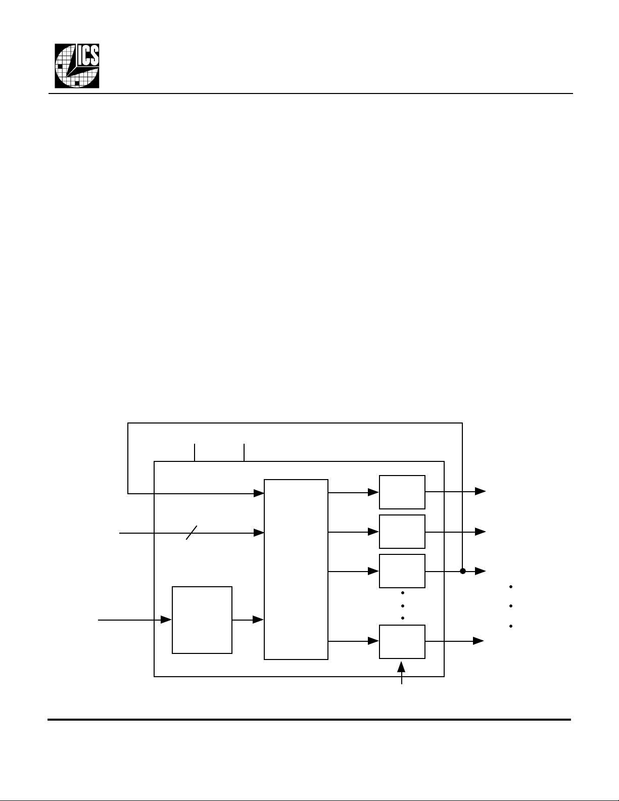
Description
The MK74ZD133 is a monolithic CMOS high
speed clock driver that includes an on-chip PLL
(Phase Locked Loop). Ideal for communications
and other systems that require a large number of
high-speed clocks, the unique combination of PLL
and 32 outputs can eliminate oscillators and
multiple low skew buffers. With 32 outputs
included in one device, there is also no need to
worry about chip-to-chip skew. The zero delay
modes cause the input clock rising edge to be
synchronized with all of the outputs’ rising edges.
The MK74ZD133 has a large selection of built-in
multipliers, making it possible to run from a clock
input as low as 10 MHz and generate high
frequency outputs up to 80 MHz in the SSOP. For
speeds up to 133.33 MHz, use the LQFP package.
Block Diagram
Optional External Connection to Output 3 (for Zero Delay Mode)
Features
• 56 pin SSOP or 64 pin LQFP package
• On-chip PLL generates output clocks up to
80 MHz (SSOP) or 133.33 MHz (LQFP)
• Zero delay plus multiplier function
• 32 low-skew outputs can eliminate chip-to-chip
skew concerns in systems with less than 33 clocks
• Output to output skew of 200 ps (with stagger)
• Device to device skew of 700ps
• Staggered, fixed skew helps reduce EMI
• Tri-state (Output Enable) pin
• Output blocks can be independently powered off
• 250 ps typical fixed delay between input and
output in “Multiplier” mode
• Ideal for Fast Ethernet and Gigabit Ethernet
designs
• Good for video servers
• 3.3V±5% supply voltage
VDD
FBIN
S4:0
Clock input
MDS 74ZD133 C 1 Revision 010899 Printed 11/17/00
Integrated Circuit Systems, Inc.•525 Race Street•San Jose•CA•95126•(408)295-9800tel•www.icst.com
5
Input
Buffer
GND
Clock
Synthesis
Circuitry
Output
Buffer
Output
Buffer
Output
Buffer
Output
Buffer
OE (all outputs)
Output 1
Output 2
Output 3
Output 32
Page 2
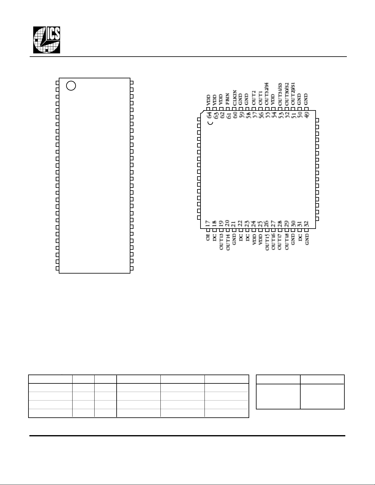
Pin Assignments
PRELIMINARY
PRELIMINARY
INFORMATION
INFORMATION
MK74ZD133
PLL and 32-Output Clock Driver
OUT1
OUT2
GND
CLKIN
FBIN
VDD
VDD
FBOUT3
OUT4
GND
OUT5
OUT6
VDD5:8
OUT7
OUT8
GND
OUT9
OUT10
VDD9:12
OUT11
OUT12
GND
VDD13:14
OE
OUT13
OUT14
GND
VDD
1
2
3
4
5
6
7
8
9
10
11
12
13
14
15
16
17
18
19
20
21
22
23
24
25
26
27
28
SSOP
56
55
54
53
52
51
50
49
48
47
46
45
44
43
42
41
40
39
38
37
36
35
34
33
32
31
30
29
OUT32/S4
VDD
OUT31/S3
OUT30/S2
OUT29/S1
GND
VDD
OUT28/S0
OUT27
OUT26
OUT25
GND
OUT24
OUT23
VDD21:24
OUT22
OUT21
GND
OUT20
OUT19
VDD
VDD
GND
OUT18
OUT17
OUT16
OUT15
VDD
FBOUT3
OUT4
GND
OUT5
OUT6
VDD5:8
OUT7
OUT8
GND
OUT9
OUT10
VDD9:12
OUT11
OUT12
GND
VDD13:14
1
2
3
4
5
6
7
8
LQFP
9
10
11
12
13
14
15
16
Y Package 10mm x 10mm x 1.4mm
48
47
46
45
44
43
42
41
40
39
38
37
36
35
34
33
VDD
OUT28/S0
OUT27
OUT26
OUT25
GND
OUT24
OUT23
VDD21:24
OUT22
OUT21
GND
OUT20
OUT19
VDD
VDD
F Package 300 mil wide
Controlling the Output Blocks
The MK74ZD133 offers a unique power supply structure that effectively creates five separate blocks of
outputs. The main supply (VDD) goes to all internal circuitry and to 18 outputs, as shown in the Pin
Descriptions table. The other 14 outputs are split into 4 blocks that are powered independently of the main
VDD supply. Each block has its own supply which can be the same as VDD, less than VDD, or left
unpowered to shut off the corresponding outputs. For example, with VDD = 3.3 V, VDD5:8 can be
unconnected and the OUT5:8 levels will be floating. The table below summarizes the power supply control
of the MK74ZD133.
VDD Name F Pin # Y Pin # Output Name F Pin Numbers Y Pin Numbers
VDD5:8 13 6 OUT5:8 11, 12, 14, 15 4, 5, 7, 8
VDD9:12 19 12 OUT9:12 17, 18, 20, 21 10, 11, 13, 14
VDD13:14 23 16 OUT13:14 25, 26 19, 20
VDD21:24 42 40 OUT21:24 40, 41, 43, 44 38, 39, 41, 42
MDS 74ZD133 C 2 Revision 010899 Printed 11/17/00
Integrated Circuit Systems, Inc.•525 Race Street•San Jose•CA•95126•(408)295-9800tel•www.icst.com
F Main Supply Y Main Supply
6, 7, 28, 29 24, 25, 33, 34
35, 36, 50, 55 48, 54, 62, 63
and 64
Page 3
PRELIMINARY
PRELIMINARY
INFORMATION
INFORMATION
MK74ZD133
PLL and 32-Output Clock Driver
Pin Descriptions for 56 pin SSOP (F package)
Number Name Type Description
1, 2, 9 OUT1, 2, and 4 O Clock outputs 1, 2 and 4.
3, 10, 16, 22, 27 GND P Connect to ground.
4 CLKIN I Clock input for reference.
5 FBIN I Feedback input for "zero delay" in Multiplier Mode.
6, 7,28,29,35,36,50,55 VDD P Power supply for internal circuits and OUT1:4, OUT15:20, and OUT25:32.
8 FBOUT3 O Clock output 3. Connect to pin 5 for Zero Delay Mode.
11, 12, 14, 15 OUT5-OUT8 O Clock outputs 5 through 8; level set by VDD5:8 on pin 13.
13 VDD5:8 P Power supply for outputs 5 through 8. Cannot exceed VDD.
17, 18, 20, 21 OUT9-OUT12 O Clock outputs 9 through 12; level set by VDD9:12 on pin 19.
19 VDD9:12 P Power supply for outputs 9 through 12. Cannot exceed VDD.
23 VDD13:14 P Power supply for outputs 13 and 14. Cannot exceed VDD.
24 OE (see note) I Output Enable. Tri-states all clock outputs when low. Internal pull-up.
25, 26 OUT13-OUT14 O Clock outputs 13 and 14; level set by VDD13:14 on pin 23.
30, 31, 32, 33, 37, 38 OUT15-OUT20 O Clock outputs 15 through 20.
34, 39, 45, 51 GND P Connect to ground.
40, 41, 43, 44 OUT21-OUT24 O Clock outputs 21 through 24; level set by VDD21:24 on pin 42.
42 VDD21:24 O Power supply for outputs 21 through 24. Cannot exceed VDD.
46, 47, 48 OUT25-OUT27 O Clock outputs 25 through 27.
49 OUT28/S0 I/O Clock output 28 and output frequency select 0 per table on page 5.
52 OUT29/S1 I/O Clock output 29 and output frequency select 1 per table on page 5.
53 OUT30/S2 I/O Clock output 30 and output frequency select 2 per table on page 5.
54 OUT31/S3 I/O Clock output 31 and output frequency select 3 per table on page 5.
56 OUT32/S4 I/O Clock output 32 and output frequency select 4 per table on page 5.
Type: I = Input, O = output, P = power supply connection, I/O=input upon power up, becoming an output
clock within 10 ms later.
Important Note for OE functionality: To use the output enable function, once the OE has been taken
low, and the outputs have been tri-stated, the VDD must be removed and reapplied for the clocks to run
again.
Staggered output skews for 56 pin SSOP (F) To aid in the reduction of EMI, and to allow the board
designer the flexibility of running different length traces whose clock edges will still line up at their
destinations, the MK74ZD133F comes with different fixed skews for different outputs. All skews are with
respect to OUT1 (pin 1), and are measured into 33Ω termination resistors with 15 pF capacitive loads.
Output Name Pin Numbers Typical Skew Maximum variation
OUT2, OUT25:32 2, 46:49, 52:54, 56 0 200 ps
OUT4, OUT18:24 9, 33, 37, 38, 40, 41, 43, 44 - 350 ps 200 ps
OUT3, OUT5:8, OUT13:17 8, 11, 12, 14, 15, 25, 26, 30:32 -225 ps 200 ps
OUT9:12 17, 18, 20, 21 -150 ps 200 ps
MDS 74ZD133 C 3 Revision 010899 Printed 11/17/00
Integrated Circuit Systems, Inc.•525 Race Street•San Jose•CA•95126•(408)295-9800tel•www.icst.com
Page 4

PRELIMINARY
PRELIMINARY
INFORMATION
INFORMATION
MK74ZD133
PLL and 32-Output Clock Driver
Pin Descriptions for 64 pin LQFP (Y package)
Number Name Type Description
1 FBOUT3 O Clock output 3. Connect to pin 61 FBIN for Zero Delay Mode.
2, 56, 57 OUT4, 1, and 2 O Clock outputs 4, 1 and 2 respectively.
3, 9, 15, 21, 30, 32 GND P Connect to ground.
4, 5, 7, 8 OUT5-OUT8 O Clock outputs 5 through 8; level set by VDD5:8 on pin 6.
6 VDD5:8 P Power supply for outputs 5 through 8. Cannot exceed VDD.
10, 11, 13, 14 OUT9-OUT12 O Clock outputs 9 through 12; level set by VDD9:12 on pin 12.
12 VDD9:12 P Power supply for outputs 9 through 12. Cannot exceed VDD.
16 VDD13:14 P Power supply for outputs 13 and 14. Cannot exceed VDD.
17 OE (see note) I Output Enable. Tri-states all clock outputs when low. Internal pull-up.
18, 22, 23, 31 DC - Don't Connect. Do not connect anything to these pins.
19, 20 OUT13-OUT14 O Clock outputs 13 and 14; level set by VDD13:14 on pin 16.
24, 25, 33, 34 VDD P Power supply for internal circuits and OUT1:4, OUT15:20, and OUT25:32.
26, 27, 28, 29, 35, 36 OUT15-OUT20 O Clock outputs 15 through 20.
37, 43, 49, 50, 58, 59 GND P Connect to ground.
38, 39, 41, 42 OUT21-OUT24 O Clock outputs 21 through 24; level set by VDD21:24 on pin 40.
40 VDD21:24 P Power supply for outputs 21 through 24. Cannot exceed VDD.
44, 45, 46 OUT25-OUT27 O Clock outputs 25 through 27.
47 OUT28/S0 I/O Clock output 28 and output frequency select 0 per table on page 5.
48, 54, 62, 63, 64 VDD P Power supply for internal circuits and OUT1:4, OUT15:20, and OUT25:32.
51 OUT29/S1 I/O Clock output 29 and output frequency select 1 per table on page 5.
52 OUT30/S2 I/O Clock output 30 and output frequency select 2 per table on page 5.
53 OUT31/S3 I/O Clock output 31 and output frequency select 3 per table on page 5.
55 OUT32/S4 I/O Clock output 32 and output frequency select 4 per table on page 5.
60 CLKIN I Clock input for reference.
61 FBIN I Feedback input for "zero delay" in Multiplier Mode.
Type: I = Input, O = output, P = power supply connection, I/O=input upon power up, becoming an output clock within 10 ms later.
Important Note for OE functionality: To use the output enable function, once the OE has been taken low,
and the outputs have been tri-stated, the VDD must be removed and reapplied for the clocks to run again.
Staggered output skews for 64 pin LQFP (Y) To aid in the reduction of EMI, and to allow the board
designer the flexibility of running different length traces whose clock edges will still line up at their
destinations, the MK74ZD133Y comes with different fixed skews for different outputs. All skews are with
respect to OUT1 (pin 56), and are measured into 33Ω termination resistors with 15 pF capacitive loads.
Output Name Pin Numbers Typical Skew Maximum variation
OUT1, OUT25:32 56, 44, 45, 46, 47, 51, 52, 53, 55 0 200 ps
OUT2,3, OUT5:14, OUT23,24 57, 1, 4, 5, 7, 8,10,11,13,14, 19,20,41,42 - 150 ps 200 ps
OUT4, OUT15:22 2, 26, 27, 28, 29, 35, 36, 38, 39 - 300 ps 200 ps
MDS 74ZD133 C 4 Revision 010899 Printed 11/17/00
Integrated Circuit Systems, Inc.•525 Race Street•San Jose•CA•95126•(408)295-9800tel•www.icst.com
Page 5

PRELIMINARY
PRELIMINARY
INFORMATION
INFORMATION
MK74ZD133
PLL and 32-Output Clock Driver
Output Frequency Select Table
Address S4 S3 S2 S1 S0 Input (F) Input (Y) Output
0 0 0 0 0 0
1 0 0 0 0 1
2 0 0 0 1 0
3 0 0 0 1 1
4 0 0 1 0 0
5 0 0 1 0 1
6 0 0 1 1 0
7 0 0 1 1 1
8 0 1 0 0 0
9 0 1 0 0 1
10 0 1 0 1 0
11 0 1 0 1 1
12 0 1 1 0 0
13 0 1 1 0 1
14 0 1 1 1 0
15 0 1 1 1 1
16 1 0 0 0 0
17 1 0 0 0 1
18 1 0 0 1 0
19 1 0 0 1 1
20 1 0 1 0 0
21 1 0 1 0 1
22 1 0 1 1 0
23 1 0 1 1 1
24 1 1 0 0 0
25 1 1 0 0 1
26 1 1 0 1 0
27 1 1 0 1 1
28 1 1 1 0 0
29 1 1 1 0 1
30 1 1 1 1 0
31 1 1 1 1 1
20 20 90*
20 20 30
20 20 81*
20 20 25
20 20 54
20 20 50
20 20 33.33
20 20 27
20 20 64
20 20 75
20 20 83.33*
20 20 66.66
20 20 133.33*
20 20 62.5
20 20 31.25
20 20 125*
20 20 55
20 20 53.125
20 20 135*
20 20 106.25*
20 20 106*
20 20 106.25*
20 20 106.66*
20 20 107*
7 - 26.5 7 - 44.44 x3
3 - 10 3 - 16.67 x8
4 - 13.33 4 - 22.22 x6
5 - 16 5 - 26.67 x5
reserved reserved reserved
10 - 40 10 - 66.67 x2
6 - 20 6 - 33.33 x4
20 - 80 20 - 100 x1
Output Frequency Generation
The MK74ZD133 has two primary
modes of operation: “Clock Generator”
and “Zero Delay Multiplier”.
In Clock Generator mode, addresses 0
through 23, specific output frequencies
are generated from a 20 MHz input.
There is no fixed phase relationship
between the input and output clocks.
In Zero Delay Multiplier mode,
addresses 24 through 31, the output
frequency is a simple integer multiple of
the input. The input range can vary over
several MHz, making it possible to
generate output frequencies that are not
included in Clock Generator mode. In
this mode, FBOUT3 is fed back to the
FBIN pin, and the rising edges of the
input and outputs are synchronized.
Configuring the Input/Output
Pins
The MK74ZD133 uses I/O pins whose
status as select inputs are sampled upon
power-up. The chip then selects this
address in the table to the left, and stays
in that configuration until a new powerup sequence, when the select inputs are
sampled again. These pins all have
internal pull-up resistors, so the 10kΩ
resistor is only needed to connect to
ground for the 0 selection in the table
(as shown below).
* These modes only guaranteed in the Y (LQFP) package
For select
= 0 (low)
I/O
33Ω
to load
10kΩ
Don’t stuff 10k
for“1” selection
MDS 74ZD133 C 5 Revision 010899 Printed 11/17/00
Integrated Circuit Systems, Inc.•525 Race Street•San Jose•CA•95126•(408)295-9800tel•www.icst.com
Page 6

PRELIMINARY
ABSOLUTE MAXIMUM RATINGS (Note 1)
DC CHARACTERISTICS (VDD = 3.3 V unless noted)
AC CHARACTERISTICS (VDD = 3.3 V unless noted)
The MK74ZD133 requires some inexpensive external components for proper operation. Decoupling
capacitors of 0.01µF should be connected on each VDDxx pin to ground, as close to the device as possible
(adjacent VDDs can be connected together). A series termination resistor of 33Ω must be used for each
clock output. See the discussion on page 5 for other external resistors required for proper I/O operation.
PRELIMINARY
INFORMATION
INFORMATION
MK74ZD133
PLL and 32-Output Clock Driver
Electrical Specifications
Parameter Conditions Minimum Typical Maximum Units
Supply Voltage, VDD Referenced to GND 7 V
Inputs Referenced to GND 0.5 VDD+0.5 V
Clock Outputs Referenced to GND 0.5 VDD+0.5 V
Ambient Operating Temperature 0 70 C
Soldering Temperature Max of 10 seconds 260 C
Storage Temperature -65 150 C
Operating Voltage, VDD 3.15 3.3 3.45 V
Required External VDD Power Supply Ramp To 90% VDD 0.1 50 ms
Input High Voltage, VIH (S0-S4, OE) 2.0 V
Input Low Voltage, VIL (S0-S4, OE) 0.8 V
Output High Voltage IOH=-4mA VDD-0.4 V
Output High Voltage IOH=-12mA 2.4 V
Output Low Voltage IOL=12mA 0.8 V
Operating Supply Current, IDD, at 66.6 MHz No Load, F package 135 mA
Operating Supply Current, IDD, at 133 MHz No Load, Y package 270 mA
Short Circuit Current at 3.3V Each output ±35 mA
Input Capacitance OE, FBIN, CLKIN 5 pF
Input Clock Frequency See page 5 3 80 MHz
Output Clock Frequency, F package 80 MHz
Output Clock Frequency, Y package Note 2. 133.34 MHz
Input to Output skew, Rising Edges at VDD/2 Zero Delay Mode, nt. 3 ±100 ±350 ps
Device to Device skew, VDD/2, ZD mode OUT1 to OUT1 700 ps
Output to Output skew, Rising Edges at VDD/2 Plus offsets ±150 see pages 4,5 ps
Output Clock Rise Time, into 33Ω and 15pF 0.8 to 2.0V 1.5 2 ns
Output Clock Fall Time, into 33Ω and 15pF 2.0 to 0.8V 1.5 2 ns
Total Capacitive Load on all outputs, still air 133 MHz 320 pf
Notes:
1. Stresses beyond those listed under Absolute Maximum Ratings could cause permanent damage to the device. Prolonged exposure
to levels above the operating limits but below the Absolute Maximums may affect device reliability.
2. Assumes maximum of 10 pF loads on all outputs in still air, and a thermal ground pad under the LQFP. For 15 pF loads on each
output, air circulation of TBD must be present.
3. From CLKIN to OUT1
External Components
MDS 74ZD133 C 6 Revision 010899 Printed 11/17/00
Integrated Circuit Systems, Inc.•525 Race Street•San Jose•CA•95126•(408)295-9800tel•www.icst.com
Page 7

PRELIMINARY
Inches
Millimeters
PRELIMINARY
INFORMATION
INFORMATION
Package Outline and Package Dimensions for
56 pin SSOP
E H
h x 45°
D
MK74ZD133
PLL and 32-Output Clock Driver
56 pin SSOP - F package
Symbol Min Max Min Max
A 0.095 0.110 2.413 2.794
b 0.008 0.013 0.203 0.343
c 0.005 0.010 0.127 0.254
D 0.720 0.730 18.288 18.542
E 0.292 0.299 7.417 7.595
H 0.400 0.410 10.160 10.414
e
L 0.024 0.040 0.610 1.016
Q 0.008 0.016 0.203 0.406
Q
e
c
b
Package Outline for 64 pin LQFP
D
D1
E1
e
A
L
A2
A
E
B
A1
1.00
REF.
L
MDS 74ZD133 C 7 Revision 010899 Printed 11/17/00
Integrated Circuit Systems, Inc.•525 Race Street•San Jose•CA•95126•(408)295-9800tel•www.icst.com
Page 8

PRELIMINARY
JEDEC VARIATION (All dimensions in millimeters)
PRELIMINARY
INFORMATION
INFORMATION
MK74ZD133
PLL and 32-Output Clock Driver
Package Dimensions for 64 Pin LQFP
S
Y
M
B
O
L
A 1.60
A1 0.05 0.15
A2 1.35 1.40 1.45
D 12.00 BSC.
D1 10.00 BSC.
E 12.00 BSC.
E1 10.00 BSC.
L 0.45 0.60 0.75
N 64
e 0.50 BSC.
b 0.17 0.22 0.27
b1 0.17 0.20 0.23
ccc 0.08
ddd 0.08
MIN. NOM. MAX.
BCD
Layout Information for 64 pin LQFP
Due to the large number of outputs capable
of running high speeds, the LQFP package
has an integrated heat slug to dissipate power.
When running the device above 105 MHz, or
with heavy (>15 pF) capacitive loads, it is
recommended to include a copper ground
pad, without anti-solder coating, underneath
the device. This will allow the PC board to
help in dissipating the heat created by the
MK74ZD133Y.
Ordering Information
Part/Order Number Marking Package Temperature
MK74ZD133F MK74ZD133F 56 pin SSOP in tubes 0 to 70 C
MK74ZD133FT MK74ZD133F 56 SSOP in Tape & Reel 0 to 70 C
MK74ZD133Y MK74ZD133Y 64 pin LQFP in trays 0 to 70 C
MK74ZD133YT MK74ZD133Y 64 LQFP in Tape & Reel 0 to 70 C
While the information presented herein has been checked for both accuracy and reliability, Integrated Circuit Systems, Inc. (ICS) assumes no responsibility for either its use or for
the infringement of any patents or other rights of third parties, which would result from its use. No other circuits, patents, or licenses are implied. This product is intended for use
in normal commercial applications. Any other applications such as those requiring extended temperature range, high reliability, or other extraordinary environmental requirements
are not recommended without additional processing by ICS. ICS reserves the right to change any circuitry or specifications without notice. ICS does not authorize or warrant any
ICS product for use in life support devices or critical medical instruments.
MDS 74ZD133 C 8 Revision 010899 Printed 11/17/00
Integrated Circuit Systems, Inc.•525 Race Street•San Jose•CA•95126•(408)295-9800tel•www.icst.com
 Loading...