

Page 1
MK715
Touch Screen Controller
General Description
The MK715 Touch Screen Controller IC provides all the
screen drive, Analog to Digital converter (ADC) and
control circuits to easily interface to 4-wire analog resistive
touch screens. It also includes a general purpose A to D
converter and a clock synthesizer.
The IC continually monitors the screen waiting for a
touch. In this mode, the supply current is typically 4µA.
When the screen is touched, the IC performs analog to
digital conversions to determine the location of the touch,
stores the X and Y locations in the registers, and issues
an interrupt. This process is repeated up to 303 times per
second until no further screen touches are detected, at
which time the low current mode is resumed.
The device has a general purpose input into the 10-bit
ADC, allowing for the measurement of other inputs such
as battery voltage. The MK715 can be powered from a
3.3V supply, and uses an inexpensive 32.768kHz watch
crystal as the input reference. An internal Phase-Lock
Loop clock synthesizer provides the high speed clock for
the ADC, and the option to have a clock output to drive
other digital chips in the system.
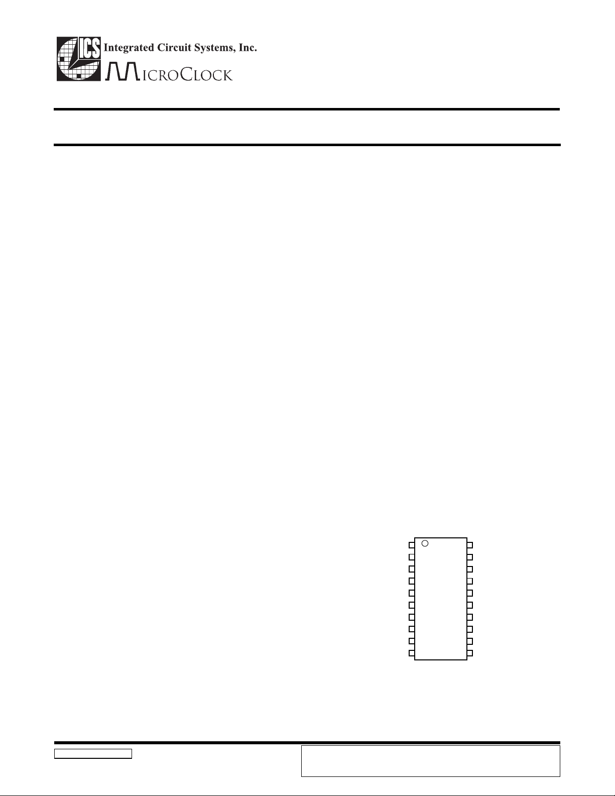
The tiny package is the same body size as the 14 pin
SOIC, with 25 mil spacings on the leads.
Features
Tiny 20 pin SSOP (150 mil body)
4 microamp standby current
Less than 3mA active current at 3.3V, including
screen drive
Touch pressure can be measured
One or two general purpose A to D inputs
On-chip voltage reference
32.768kHz crystal/clock input
MHz clock outputs available
Operates with four wire touch screens
Ratiometric conversion eliminates screen
calibration
Automatic wake up upon screen touch
Programmable conversion rate to a maximum of
303 points per second
3.3V or 5V supply (2.7V version available)
10 bit A/D converter
Full powerdown control
Touch screen is directly driven - no external
transistors are required
A to D Converter guaranteed monotonic
3 or 4 wire serial interface
Applications
Notebook Computers
Handheld Computers
PDAs
Touch-screen kiosks
MK715RevD020200
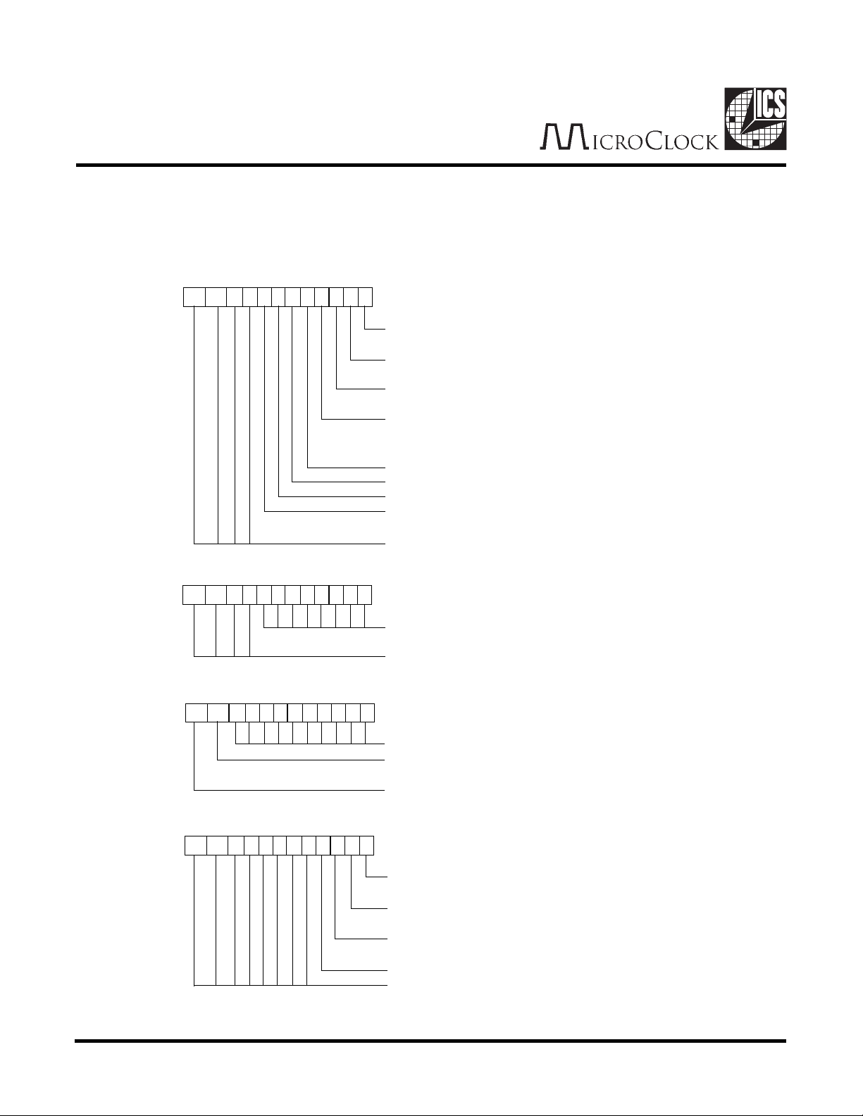
Pin Assignment
CS
SK
1
D0
2
DI
3
TOUCH#
XH
XL
YH
YL
PL
GP
4
5
6
7
8
9
10
MK715
20 pin SSOP
ICS reserves the right to make changes in the device data identified in this publication
without further notice. ICS advises its customers to obtain the latest version of all device
data to verify that any information being relied upon by the customer is current and accurate.
20
19
18
17
16
15
14
13
12
11
CLKOUT
INT
VDD
X2
X1
GND
CAP2
CAP1
CAP3
Page 2
MK715
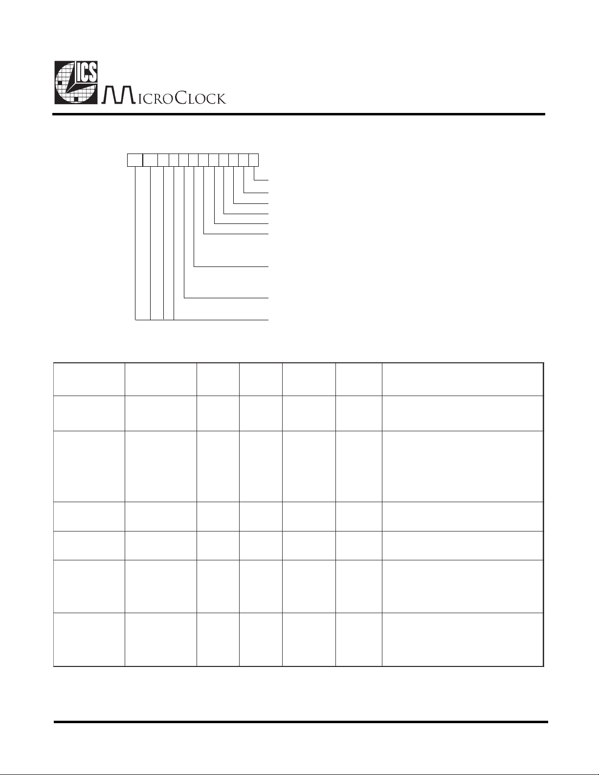
Pin Descriptions
#niPemaNepyTnoitpircseD
1KSI .kcolClaireS
2ODO .3nipottcennoc,troplaireseriw3roF.tuOataD
3IDI .2nipottcennoc,troplaireseriw3roF.nIataD
4#HCUOTO .tuokcolClanoitpO.dehcuotsineercsnehwwolseoG.langiShcuoT
5HXST.)edisthgir(neercshcuotnohgih-XottcennoC
6LXST.)edistfel(neercshcuotnowol-XottcennoC
7HYST.)pot(neercshcuotnohgih-YottcennoC
8LYST.)mottob(neercshcuotnowol-YottcennoC
9LPI .tupniCDAesopruplareneG
01PGI .tupniCDAesopruplareneG
113PAC- .dnuorgotroticapacFu10.0atcennoC
211PAC- .noitcennocretlifpooL
312PAC- .noitcennocretlifpooL
41DNGP .dnuorgottcennoC
511XI .tupnikcolcrofdnuorgro,latsyrczHk867.23ottcennoC
612XI .tupnikcolcrolatsyrczHk867.23ottcennoC
71DDVP .V3.3+roV5+ottcennoC
81TNIO .tuptuokcolclanoitpO.tpurretnilangisothgihseoG.tpurretnI
91TUOKLCO .tuptuozHMeboslanaC.zHk867.23yllacipyT.tuptuokcolC
02SCI .hgihevitcAtcelespihC
Key: I = Input, O = Output, I/O = Input and Output, P = Power, TS = Touch Screen pin.
2
Page 3

MK715
Chip Overview
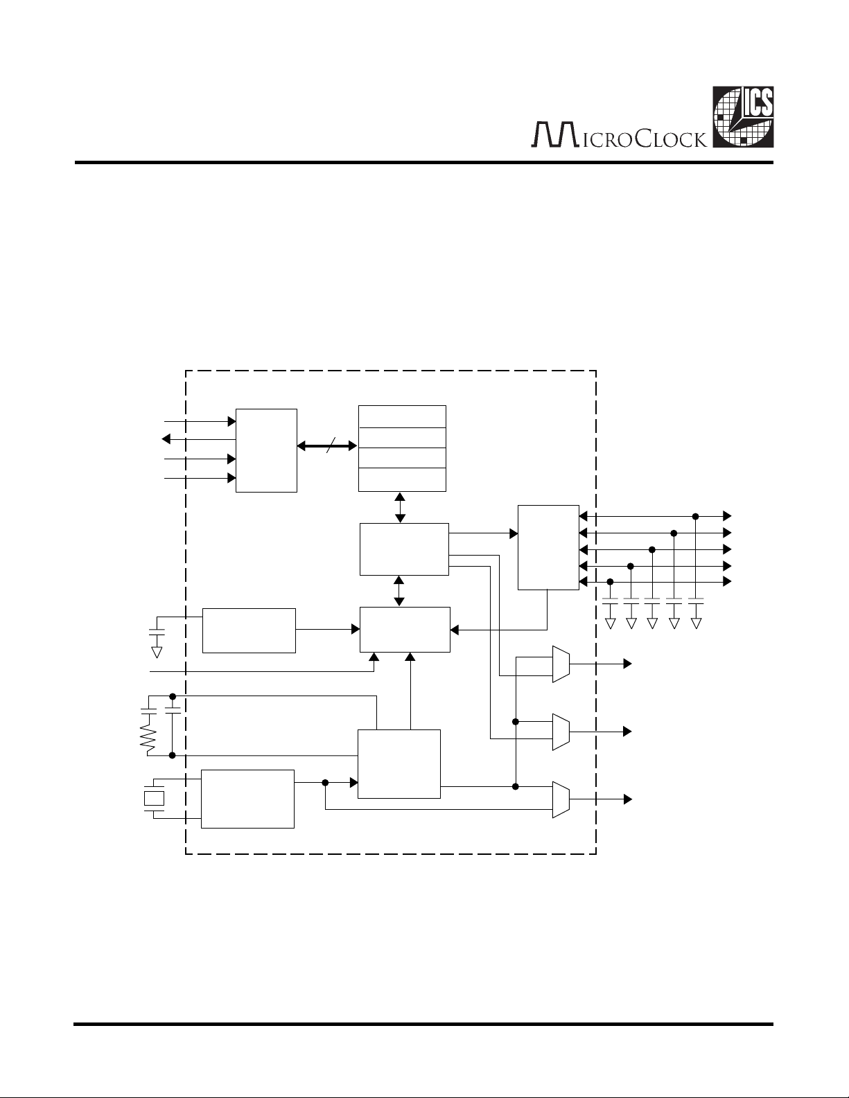
The MK715 communicates via a 4 pin serial port. This may be connected as either a 3 or 4 wire
serial port. The port is connected to 4 registers that control the various modes and function of the
chip.
The primary function of the MK715 is to control resistive touchscreens. There are two ways to read
screen points, both controlled by the registers.
In the first method, which is enabled by setting the ENCONR bit, the MK715 performs periodic
conversions at a rate set by the rate register. The chip monitors the touch screen in a low power
condition (about 4 mA) until the screen is touched. When a touch is detected, the chip powers up
and starts converting screen points. The TOUCH# pin goes low and INT goes high to indicate a
change in touch status. The converter outputs a Y co-ordinate, then an X co-ordinate, then a Y coordinate, and so on. The X and Y co-ordinates are stored in the same register (RESULT) and each
conversion over-writes the previous conversion. When a co-ordinate is stored, the conversion
complete bit is asserted in the STATUS register. This bit is cleared when the RESULT register is
read. The inverted state of the TOUCH# pin also appears in the STATUS register. After each coordinate conversion, INT goes high and the screen is checked to see if it is still touched. If not,
conversions stop, TOUCH# goes high, INT goes high (to indicate a change in touch status) and
the chip reverts to the low power mode.
The second method to read a screen is to set the RD1PT (read one point) bit in the CONTROL
register. The chip will perform two conversions, a Y co-ordinate followed by an X co-ordinate. The
X co-ordinate overwrites the Y co-ordinate and so the X co-ordinate must be read before this
happens. Finally, RD1PT is cleared. The conversion pair takes about 3.5 ms.
The converter may also be used to measure voltages presented on the GP or PL pins. The range
of the converter is 0 to 1.279 V and so voltages outside this range must be scaled appropriately.
Again, the RD1PT bit is set to start the conversion but first either SELGP or SELPL must be set
to select the correct input. Only one conversion is performed. The result is stored in the RESULT
register and then RD1PT is cleared. The conversion takes about 1.7ms.
The final conversion mode is used to measure touch pressure. This is controlled identically to the
second method outlined above except that either RDPRESA or RDPRESB must first be set.
The MK715 allows for several different clocks to be generated, controlled by the registers. On the
CLKOUT pin, the output is either a a 32768 Hz clock from the crystal oscillator or a MHz - frequency
clock synthesized from the PLL. Similarly, this MHz - frequency clock can appear on the INT or
TOUCH# pins instead of their usual functions. In these cases, if the MHz clock needs to run
continuously, then the ENPLL bit must be set in order to override the automatic powerdown of the PLL.
Refer to page 12 for more details.
3
Page 4
MK715
Block Diagram
Registers
CAP3
GP
CAP1
CAP2
DI
D0
CS
SK
X1
X2
Serial
Port
Voltage
Reference
32.768kHz
Oscillator
12
Status
Rate
Result
Control
Controller
10 Bit A-D
Converter
Phase
Locked
Loop
0
1
2
3
XH
Screen
Drive
1
0
1
0
1
0
INT
TOUCH#
CLKOUT
XL
YH
YL
PL
4
Page 5
MK715
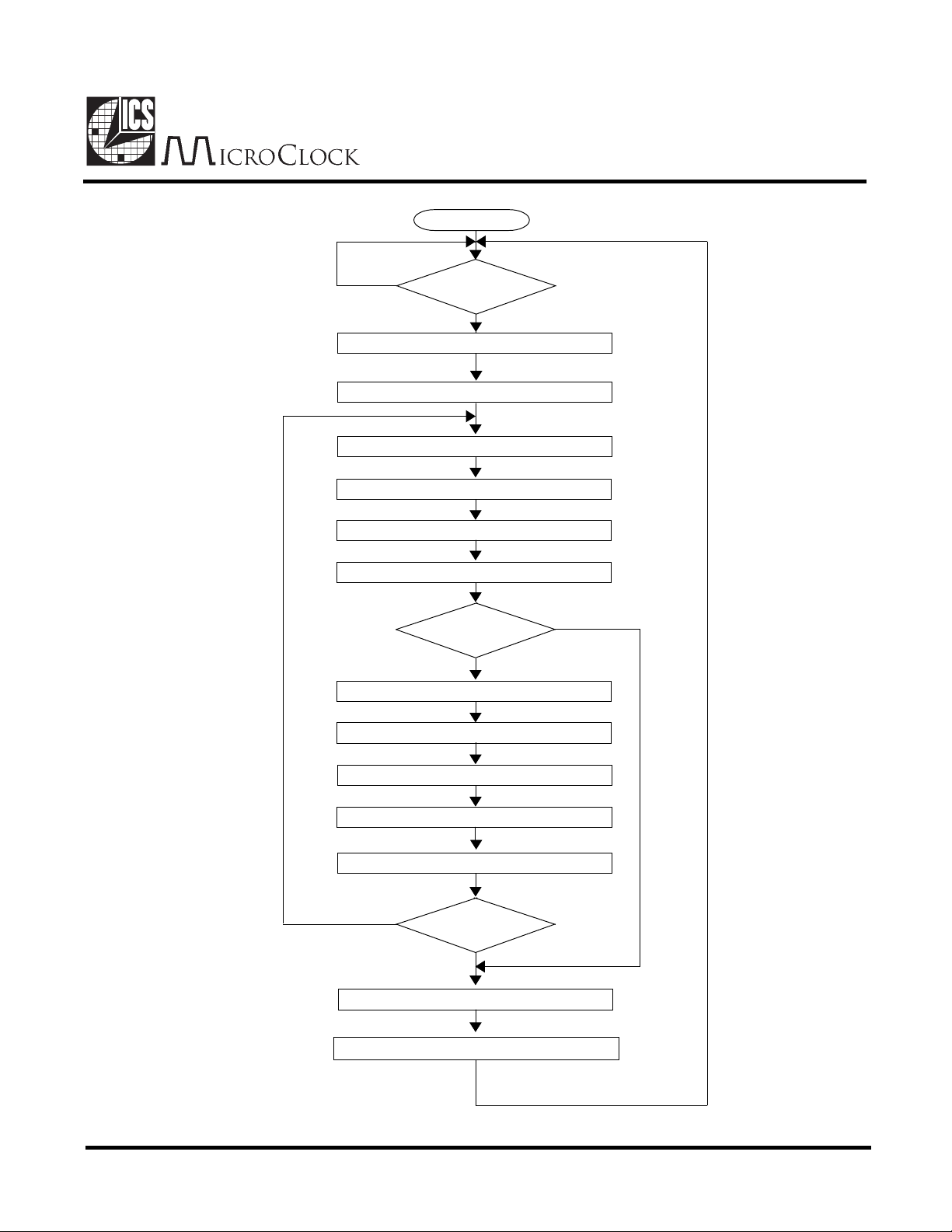
IC Operation
(Periodic Conversions Enabled)
Power ON
N
Is screen
touched?
Y
Write D6 Reg 0 to 1 and TOUCH# = 0
Issue Interrupt, power-up ADC and PLL
Convert Y co-ordinates
Store Y co-ordinates in Register 2
Write D7 register 0 to 1
Issue interrupt
Is screen
touched?
N
Y
Convert X co-ordinates
Store X co-ordinates in Register 2
Write D7 register 0 to 1
Issue Interrupt
Wait. Duration controlled by Rate Register
Y
Is screen
touched?
N
Write D6 Reg 0 to 0 and TOUCH# = 1
Issue Interrupt, power-down ADC and PLL
5
Page 6
MK715
Register Description
The MK715 has four 12 bit registers. However, only 8 bits in each register can be written (D0-D7). The other 4 bits (D8D11) can never be written and are always read only.The RESULT register contains 2 levels, a read only level and a write
only level. Reading this register gives the conversion results. Writing this register changes 4 control bits.
DESCRIPTION
Read
and
Write
Read
and
Write
STATUS (ADDRESS 0)
11 10 9 8 7 6 5 34210
RATE (ADDRESS 1)
11 10 9 8 7 6 5 34210
RD1PT. Read one point. Cleared when
conversion complete.
ENCONR. Enable periodic screen conversions
at rate set by RATE register.
PD. Power Down. Chip powers down. See
CONTROL register bit 7.
ENPLL. Overrides automatic powerdown of
PLL between conversions and forces
continuous running.
SELGP. Select GP input to ADC.
SELPL. Select PL input to ADC.
Touch Status. 1 = touch.
Conversion complete. Cleared on next read
of RESULT register.
Always set to zero.
Controls frequency of screen conversions
when periodic conversions are enabled.
Always set to zero.
TYPE
R/W
R/W
R/W
R/W
R/W
R/W
RO
RO
RO
R/W
RO
Power-up
State
0
0
0
0
0
0
0
0
0
32
0
Read
Write
RESULT (ADDRESS 2)
11 10 9 8 7 6 5 34210
RESULT (ADDRESS 2)
11 10 9 8 7 6 5 34210
10-bit conversion result.
XSEL. Screen conversion status. 0 = Y
coordinate, 1 = X coordinate.
Conversion type. 0 = non-screen
conversion, 1 = screen conversion.
RDPRESA. Read pressure A. See
description of measuring touch pressure.
RDPRESB. Read pressure B. See
description of measuring touch pressure.
PLZERO. Forces PL pin to ground. Can be
used to control an external resistor divider.
Test mode. ALWAYS WRITE TO 0.
Don't Care.
6
RO
RO
RO
WO
WO
WO
WO
-
X
0
1
0
0
0
0
X
Page 7
Register Description (cont.)
MK715
DESCRIPTION
Read
CONTROL (ADDRESS 3)
11 10 9 8 7 6 5 34210
and
Write
SEL0. Clock select 0. See page 11.
SEL1. Clock select 1. See page 11.
SEL2. Clock select 2. See page 11.
SEL3. Clock select 3. See page 11.
SEL4. Clock select 4. See page 11.
CLKSEL. Clock frequency select.
See page 11. 0 = 14.3196 MHz
1 = 14.7456 MHz
Set to 0.
DIS32. Determines state of 32.768 kHz
oscillator when PD asserted (STATUS register).
Always set to zero.
R/W = Read/Write, RO = Read Only, WO = Write Only
Converter Control
BSERPDRASERPDRLPLESPGLESRNOCNETP1DRDEMROFREPNOISREVNOC
000001ot0
000010
TYPE
R/W
R/W
R/W
R/W
R/W
R/W
R/W
R/W
RO
Power-up
State
0
0
0
0
0
0
0
0
0
ehtnosnoisrevnoc2smrofreP
XnanehtdnaYa-neercs
.deraelcnehtsiTP1PR.noisrevnoc
tessaetartasnoisrevnocelbanE
sineercsnehW.retsigerETARni
setareporetrevnoc,dehcuot
sihcuotonlitnuylsuonitnoc
yllacitamotuanehtpihC.detceted
.etatsybdnats,rewopwolotseog
000101ot0
001001ot0
010001ot0
.deraelc
100001ot0
.deraelc
PGnonoisrevnocenosmrofreP
.deraelcsiTP1DR.tupni
LPnonoisrevnocenosmrofreP
.deraelcsiTP1DR.tupni
dnaYa,snoisrevnocowtsmrofreP
erusserphcuotevigot,Xnaneht
hcuotnonoitceseeS.atad
siTP1DR.tnemerusaemerusserp
dnaYa,snoisrevnocowtsmrofreP
erusserphcuotevigot,Xnaneht
hcuotnonoitceseeS.atad
siTP1DR.tnemerusaemerusserp
The converter must be sequenced correctly - before writing RD1PT to one, the appropriate bit (e.g. SELGP) must
first be set in a previous write. Only the combinations shown above are permitted. Other combinations will give
unpredictable behavior.
7
Page 8

MK715
Rate Register (Register 2) Programming
tnuoC.S.P.PtnuoC.S.P.PtnuoC.S.P.P
5ot0dettimreptoN527115804
6303623110983
7082729015963
89528260100143
92429230150123
017220300101113
11312138951103
21102235902192
31191333952182
41181430953162
51271538854142
61561048755122
71751541756112
81151054657102
91541559558191
02931065559181
12431561550271
22921077451261
32521575453251
42021082455241
P.P.S. = Points Per Second. With 14.7456 MHz clock selected.
Calculating Points Per Second
The formula for determining P.P.S. is:
P.P.S. =
fin
24072+(4096×COUNT)
Where fin is the frequency of the
internal clock (14.3196 MHz or
14.7456 MHz) and COUNT is
the value of the rate register.
Power-On Reset
On application of power, an internal reset is generated that clears all bits in registers 0, 2, and 3. Register 1 is set to
32 giving a rate of 92 PPS with 14.3196 MHz selected.
Initializing the MK715
The interrupt on the MK715 can only be cleared by reading any register or, alternatively, by writing PD (register 0, bit
2) to one, which forces a powerdown. After a fault condition, initialize the MK715 by writing PD to one, then writing
PD to zero. This will always clear pending interrupts.
8
Page 9

MK715
Warning - Operation under a Power Supply Switching Regulator
When using the MK715 in a system where the power is supplied by a switching regulator, do not perform screen
conversions when the regulator is operating in the power saving mode. Some switching regulators feature a low
power mode (for example, Linear Technology's "Burst Mode") where the output is turned on and off in order to save
power. The extra power supply noise generated when using this mode causes spurious data points to be returned
from the MK715, so it should be disabled when the MK715 is doing screen conversions.
Interrupts
The MK715 generates an interrupt to signal a change in touch status or to signal that a conversion is complete. The
INT pin (pin 2) goes high to signal an interrupt. Interrupts are then cleared by reading any register. However, if the
MK715 is in the process of generating an interrupt during a read cycle, then the interrupt is not cleared and INT will
stay high. This internal process may take 100ns, and so to guarantee that the interrupt is cleared, two successive read
cycles may be necessary.
Touch Screen Serial Port (Four Wire)
Data is written to, and read from, the MK715 via the serial port. When writing, only 8 data bits can be
written to each 12 bit register. The 4 highest order bits (D8-D11) in each register are read only and can
never be writtern. When reading, all 12 bits are returned.
The serial port has 4 pins - serial clock (SK), chip select (CS), data in (DI), and data out (DO). The SK acts on the rising
edge. The CS acts as a reset for the serial port with CS going high initiating a cycle. The cycle consists of 2 parts a write followed by a read. Each part consists of 12 bits. Refer to the serial port diagram on page 10 and timing
diagram on page 20.
After CS goes high, any number of leading zeros can occur on DI. When a one is presented (even if this is the first bit
after CS goes high), this becomes the start bit. The start bit is followed by 3 op-code bits. The first is a write bit (WR),
which determines whether the data following is actually loaded into the appropriate register or not. The next two bits
are address bits, which select 1 of 4 on-chip registers. The last 8 bits are data. If WR was low, then these data bits are
ignored.
On the fourteenth SK rising edge after a start bit, DO is released from tri-state and data is clocked out of the part. This
is the read part of the cycle. The register to be read is selected with the op-code address. The data are 12 bits long.
For the result of a conversion (which is stored in register 2), this data consists of 10 bits from the ADC, a bit identifying
an X or a Y coordinate, and a bit identifying a screen conversion or a general purpose conversion. For the other 3
registers, the data are only 8 bits long, so the 12 bit output word contains four leading zeros.
After the 12 data bits are clocked out, the DO pin stays active and bits will continue to appear until CS goes low. See
the following page for the timing diagram.
Three-Wire Serial Port
To configure the serial port for 3 wires, DI must be connected to DO to form a bi-directional data line. All other timing
and configuration remain unchanged.
9
Page 10

MK715
Using the General Purpose Inputs to the A to D Converter
The GP pin is a general purpose input to the 10 bit ADC. An on-chip 1.297 V reference is used, where 1.297 V is full
scale. In addition, when using a 4-wire touch screen, the PL pin is available as a general purpose input, or it can be
used as a power control for an external resistor divider:
Voltage to be
measured
Optional
Capacitor
For two voltages, the connection is as follows:
Voltage 1
GP
PL
SELGP
SELPL
MK715
SELGP, SELPL, and
PLZERO are all register
bits.
ADC
PLZERO
MK715
SELGP
Voltage 2
Optional
Capacitor
If PL or GP are unused, they should be connected to ground.
The capacitors connected to GP and PL are optional and will reduce noise on the ADC input.
GP
PL
ADC
SELPL
PLZERO=0
(transistor
off)
10
Page 11

MK715
Clock Control
X1
32.768kHz
X2
PD
DIS32
Clock Selection Tables
2LESDPLLPNE23SIDQERFTUOKLCSETON
00x 0 867.23etatSpu-rewoP
00x 1 867.23
01x 0 867.23
01x 1 FFO
100 x ZHM
10 1 x ZHMgninnuRsyawlA
110 x FFO
111 x FFO
PD
ENPLL
Phase
Locked
CLKSEL
To A-D Converter
/ 8
/ 4
/ 2
14.3196 or
SEL0, SEL1
3
2
1
INT
TOUCH#
CLOCKMHZ
1
SEL2
1
SEL3
1
SEL4
CLKOUT
INT
TOUCH#
nehwylnosnuR
dehcuotneercs
LESKC1LES0LESZHMKCOLC
000 6913.41
001 061.7
010 085.3
011 097.1
100 6547.41
10 1 8273.7
110 4686.3
111 2348.1
Clocks may be programmed to be on any of three pins per the description above. The clocks are controlled by the
following register bits (see register description for more details): STATUS register, bits 2 and 3; and CONTROL
register bits 0, 1, 2, 3, 4, 5, 7.
2LESTUOKCOLC
0zHk867.23
1ZHMKCOLC
4LES#HCUOT
0#HCUOT
1ZHMKCOLC
11
3LESTNI
0TNI
1ZHMKCOLC
Page 12

MK715
Power and Clock Control
The power consumed by the MK715 can be controlled by programming various register bits.
DP23SIDLLPNERNOCNE
10 X X X ffognihtyrevE0
11 X X X
0X 0 0 oN
0X 0 0 seY
0X 1 0 X
0X 0 1 oN
0X 1 1 ON
0X X 1 seY.gnitarepo.cte,LLP,CDA
neercSehtsI
?dehcuoT
noitidnoCpihCDDIlacipyT
latsyrctpecxeffognihtyrevE
fi(tuptuozHk23dnarotallicso
)detceles
latsyrctpecxeffognihtyrevE
zHk23dnarotallisco
snipTNIdna#HCUOT.tuptuo
latsyrctpecxeffognihtyrevE
zHk23dnarotallisco
snipTNIdna#HCUOT.tuptuo
latsyrctpecxeffognihtyrevE
.stuptuokcolcdnaLLP,rotallicso
otdnopsersnipTNIdna#HCUOT
.sutatsHCUOTnisegnahc
latsyrctpecxeffognihtyrevE
.stuptuokcolcdnarotallicso
latsyrctpecxeffognihtyrevE
.stuptuokcolcdnaLLP,rotallicso
4mA
4mA
.sutatshcuotnisegnahcotdnopser
04 mA
.sutatshcuotnisegnahcotdnopser
nosdneped(Am2
ycneuqerfkcolc
gnidaoldna
4mA
Am2
rewoPeeS(Am5
tnerruCylppuS
)shparg
12
Page 13

Recommended Circuit
MK715
Microprocessor
32.768 kHz
Analog Voltage
+ 3.3V or +5V
1mF
From
Crystal
0.01mF
DI
D0
CS
SK
X2
X1
PL
GP
0.01mF
470 pF
VDD
CAP3
GND
TOUCH#
CLKOUT
CAP2
100kW 0.01mF
CAP1
INT
XH
XL
YH
YL
To Power Management
To Interrupt Controller
To Microcontroller
To Touch
Screen
All 0.01mF
The capacitors connected to CAP1 and CAP3 must be low leakage, ceramic type capacitors.
Pen Bounce
When the screen is untouched, the Y plate is driven high and the X plate is driven low. When the screen is touched, the
X plate is pulled high, which is detected by the MK715. This initiates a conversion, as long as conversions at rate
(ENCONR) are enabled. Some de-bounce is provided by the time constant of the screen decoupling capacitors
combined with the screen resistance. However, once conversions have started, pen bounce will not be detected until
after the current X or Y points have been taken.
If the pen is lifted during a conversion, this will also not be detected until the conversion is complete.
13
Page 14

MK715
Optimizing Performance when Reading and Writing Registers
Reading and writing the MK715 generates digital noise that may reduce the accuracy of the A to D converter. This
noise has several causes, including board layout, and power supply voltage. By appropriately timing the register
operations, the effects of this noise can be minimized.
After an interrupt is issued or RDIPT is asserted, the MK715 allows a minimum of 1 millisecond to elapse before
initiating the conversion cycle. This allows the screen drivers to settle. For best performance, complete all register
operations within this 1ms window after an interrupt.
Resistive Touch Screen (4 Wire)
Resistive touch screens consist of 2 resistive plates that are separated by a small gap. Each plate has an electrode
at each end and when the screen is touched, the two plates are shorted together at that point.
If a voltage is applied, for example, between XL and XH, then a voltage divider is formed on the X PLATE. When the
Y PLATE is touched to the X PLATE, a voltage will be developed on the Y PLATE that is proportional to distance of
the touch from XL and XH. By accurately measuring this voltage, the position of the touch can be determined.
14
Page 15

MK715
Analog to Digital Converter Operation with a Touchscreen
The 10-bit ADC converts X and Y co-ordinates at a rate determined by register 1. The converter uses a ratiometric
technique to give absolute co-ordinates on the screen, largely independent of variations in screen resistance,
temperature or power supply voltage. The total voltage applied across the screen is defined as full-scale for the
converter (i.e. 1023) and any point touched on the screen is proportional to this. For example, if the screen is touched
exactly in the center, the converter will read 511. This feature may allow for the elimination of calibration upon startup.
However, the full scale voltage is defined at the IC pins and so any parasitic interconnect resistance will be included
in full scale. In addition, the interconnect resistances on the screen also account for up to 20% of the total resistance.
This means that approximately the bottom 10% and top 10% of full scale are inaccessible.
The converter is guaranteed to be monotonic, with no missing codes.
Board and Wire
Interconnect
XH
Full
MK715
Scale
(1023)
Screen
Interconnect
YL
XL
X
Coordinate
Screen
Screen
Interconnect
Board and Wire
Interconnect
15
Page 16

MK715
Measuring Touch Pressure
Measuring touch pressure can only be performed on 4-wire touchscreens. In normal operation, the screen drivers
force XH high and XL to ground and measure the voltage on the other plate. A schematic of this is as follows:
Voltage measured on YH is the same as at K
and L giving the X co-ordinate.
When RDPRESA is asserted, the screen drive changes as follows (XSEL=1):
Voltage measured on YH is now the voltage at
L. Voltage measured at XL is now the voltage
at K. The difference is proportional to the
touch pressure.
When RD1PT is asserted, the converter automatically performs two conversions. The status of the XSEL bit identifies
the conversions. The following table gives the four measurements available.
BSERPDRASERPDRLESXEVIRDDERUSAEMNIP
010 LX,HYHX
011 LY,HXHY
100 LX,HYLY
10 1 LY,HXLX
Both points returned
in one conversion pair.
Both points returned
in one conversion pair.
From these four measurements, the resistance of the touch can be calculated as a proportion of x-plate and y-plate
resistance. See the next section for suggestions about calculating the touch resistance. From this, the touch pressure
can be inferred. See the table on page 7 for the correct register sequencing of the converter.
16
Page 17

Calculating Touch Resistance
There are a total of six measurements possible:
BSERPDRASERPDRLESXEVIRDDERUSAEMNIPTLUSER
000 LY,HYHXC
001 LX,HXHYD
010 LX,HYHXE
011 LY,HXHYF
100 LX,HYLYG
10 1 LY,HXLXH
where the result is a number from 0 to 1023.
MK715
From simple network theory, R
D
1023
C
1023
X
D
· · (1023 - E) - RY +
1023
or R
or R
R
TOUCH
TOUCH
TOUCH
= RX · · ( - 1) where RX = X plate resistance
= RY · · ( - 1) where RY = Y plate resistance
R
=
E
TOUCH
H
can be represented in many ways, 3 are given below:
G
E
F
RY · C
1023
17
Page 18

MK715
Electrical Specifications
retemaraPsnoitidnoCmuminiMlacipyTmumixaMstinU
stuptuOkcolCdnastupnIDNGotdecnerefeR5.0-5.0+DDVV
erutarepmeTgnitarepOtneibmA 007C
erutarepmeTgniredloSsdnoces02foxaM062C
erutarepmeTegarotS 56-051C
DDV,egatloVgnitarepO 35.5V
egatloVhgiHtupnIV5=DDV2 V
LIV,egatloVwoLtupnIV5=DDV8.0V
HOV,egatloVhgiHtuptuOAm2-=HOI4.0-DDVV
HOV,egatloVhgiHtuptuO Am21=HOI,V5=DDV4.2V
LOV,egatloVwoLtuptuO Am21=LOI,V5=DDV40.V
HIV,egatloVhgiHtupnIV3.3=DDV9.1V
LIV,egatloVwoLtupnIV3.3=DDV4.0V
HOV,egatloVhgiHtuptuO Am6-=HOI,V3.3=DDV4.2V
LOV,egatloVwoLtuptuO Am6=LOI,V3.3=DDV4.0V
V5=DDVta,DDI,tnerruCylppuSgnitarepO2eton5Am
nwodrewopDDI,tnerruCylppuSgnitarepOkcolcon,1=DP2.03A
tnerruCtiucriCtrohStuptuohcaE05Am
ecnaticapaCtupnI 7Fp
noituloseR 01stib
ytiraenil-noN4eton,cinotonoM2BSL
ecnatsiseRneercShcuoT 0010002
ecnerefeRegatloVC52,V3.3=DDV662.1972.1292.1V
ycneuqerFlatsyrCrokcolCtupnI 867.23zHk
emiTesiRtuptuO V5=DDV,V0.2ot8.03sn
emITllaFtuptuO V5=DDV,V8.0ot0.23sn
)1etoN(SGNITARMUMIXAMETULOSBA
)detonsselnu(V5ROV3.3=DDV(SCITSIRETCARAHCCD
V3.3=DDVta,DDI,tnerruCylppuSgnitarepO2eton3Am
nokcolc,ybdnatsDDItnerruCylppuSgnitarepO3eton3A
±
±
)detonsselnu(V5ROV3.3=DDV(SCITSIRETCARAHCCA
m
m
W
Notes:
1. Stresses beyond those listed under Absolute Maximum Ratings could cause permanent damage to the device. Prolonged
exposure to levels above the operating limits but below the Absolute Maximums may affect device relaibility.
2. Assumes 300 W screen, 100 pps.
3. Assumes no touch.
4. With no missing codes.
18
Page 19

MK715 TIMING DIAGRAM
MK715
SK
CS
DI
DO
Tri-State
14
A
B
1234
C
D
15 16
WR A1
E
25
SK
CS
DI
DO
F
A SK Period 50 ns
B SK High TIme 15 (SK Period) -15 ns
C CS Setup to SK high 15 ns
D DI Setup to SK high 15 ns
E DI Hold from SK high 15 ns
F DO valid from SK high 20 ns
G CS hold from last SK high 50 ns
D11
Don't Care
F
D10 D9 D1 D0
G
MIN MAX
19
Page 20

MK715
20
Page 21

MK715
To
Touch
Screen
0.01µF
G
G
Pin 1
2
3
4
5
6
7
8
9
10
20
19
18
17
16
15
14
13
12
11
0.01µF
1000 pF
0.01µF
V
0.01µF
G
100kW
32768 Hz
G
G
= Connection to ground plane
V
= Connection to VDD plane
Notes: 1. All digital signals should be kept well away from pins 5, 6, 7, 8, 9, 10,
11, 12, 13, 15, 16 and any traces connected to those pins.
21
Page 22

MK715
Package Outline and Package Dimensions
(For current dimensional specifications, see JEDEC Publication No. 95.)
20 pin SSOP ( in inches)
A1 C
L
lobmySniMxaM
A350.0960.0
1A400.0010.0
B800.0210.0
C700.0010.0
D733.0443.0
E051.0751.0
eCSB520.0
H822.0442.0
L610.0050.0
B
Ordering Information
rebmuNredrO/traPgnikraMgnippihS
R517KMR517KMsebuT
RTR517KMR517KMleeRdnaepaT
L
Integrated Circuit Systems, Inc. 525 Race Street San Jose CA95126 (408)295-9800tel www.icst.com
ICS reserves the right to make changes in the device data identified in this publication
without further notice. ICS advises its customers to obtain the latest version of all device
data to verify that any information being relied upon by the customer is current and accurate.
22
 Loading...