

Page 1
MK712
ICRO
C
LOCK
Description Features
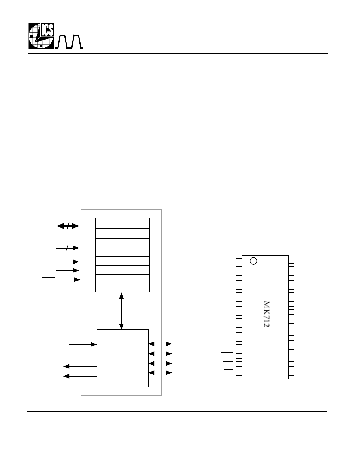
The MK712 Touch Screen Controller IC provides
all the screen drive, A to D converter and control
circuits to easily interface to 4-wire analog resistive
touch screens.
The IC continually monitors the screen waiting
for a touch. In this mode, the supply current is
typically 0.5µA. When the screen is touched, the
IC performs analog to digital conversions to
determine the location of the touch, stores the X
and Y locations in the registers, and issues an
interrupt. This process is repeated up to 197 times
per second until no further screen touches are
detected, at which time the low current mode is
resumed.
Block Diagram
8
D0-D7
3
A0-A2
CS
RD
WR
CLKIN
(14.318 MHz)
INT
TOUCH
REGISTERS
STATUS LOW
STATUS HIGH
X-LOW
X-HIGH
Y-LOW
Y-HIGH
CONTROL
RATE
12 Bit A/D,
Screen Driver
and
Controller
0
1
2
3
4
5
6
7
• Fully integrated, lowest power solution
• Low standby current of 0.5µA (typical) at 5.0V
• Active current while converting less than 10 mA
• Resolves 350 dots/inch on 10.5” display
• Maximum speed of 197 points/second
• Ratiometric conversion may eliminate screen
calibration
• Automatically wakes up and goes back to standby
• 3.3V or 5V supply
• 12 bit A/D converter
• Simplifies the writing of software for touch screens
• Extended temperature range available
• Capacitors are the only external components
required
• Touch screen is directly driven - no external
transistors are required
• Programmable conversion rate
• A to D Converter is monotonic
• Parallel interface
• See the MK715 for a serial interface
Pin Assignment
XH
XL
YH
YL
Touch Screen Controller
NC
INT
TOUCH
VDD
VDD
XH
XL
YH
YL
GND
GND
WR
RD
CS
1
2
3
4
5
6
7
8
9
10
11
12
13
14
28
27
26
25
24
23
22
21
20
19
18
17
16
15
D0
D1
D2
D3
D4
VDD
D6
D7
CLKIN
A0
A1
A2
D5
GND
MDS 712 I 1 Revision 100899 Printed 11/16/00
Integrated Circuit Systems, Inc.•525 Race St.•San Jose•CA•95126•(408)295-9800tel•www.icst.com
Page 2
MK712
ICRO
C
LOCK
Touch Screen Controller
Pin Descriptions
Number Name Type Description
1 NC - No Connect
2 INT O Interrupt. Goes high to signal an interrupt. Cleared on next read.
3 TOUCH O Touch signal. Goes low when screen is touched. Goes high when not touched.
4 VDD P Connect to +5V or +3.3V.*
5 VDD P Connect to +5V or +3.3V.*
6 XH TS Connect to X-high on touch screen. (Right side)
7 XL TS Connect to X-low on touch screen. (Left side)
8 YH TS Connect to Y-high on touch screen. (Top)
9 YL TS Connect to Y-low on touch screen. (Bottom)
10 GND P Connect to ground.
11 GND P Connect to ground.
12 WR I Write enable. Active low.
13 RD I Read enable. Active low.
14 CS I Chip select. Active low.
15 A2 I Register address 2.
16 A1 I Register address 1.
17 A0 I Register address 0.
18 CLKIN I Clock input. Typically 14.3 MHz. Best if driven by a MicroClock clock synthesizer.
19 D7 I/O Data bit 7.
20 D6 I/O Data bit 6.
21 GND P Connect to ground.
22 VDD P Connect to +5V or +3.3V.*
23 D5 I/O Data bit 5.
24 D4 I/O Data bit 4.
25 D3 I/O Data bit 3.
26 D2 I/O Data bit 2.
27 D1 I/O Data bit 1.
28 D0 I/O Data bit 0.
Key: I = Input, O = Output, I/O = Input and Output, P = Power, TS = Touch Screen pin..
*Note: All VDD’s must be connected to the same voltage.
Interrupts
Interrupts are controlled by register 6 (see Register Description). The INT pin (pin 2) goes high to
signal an interrupt. Interrupts are then cleared by reading any register. However, if the MK712 is in the
process of generating an interrupt during a read cycle, then the interrupt is not cleared and INT will stay
high. This internal process may take 100ns, and so to guarantee that the interrupt is cleared, two
successive read cycles may be necessary.
MDS 712 I 2 Revision 100899 Printed 11/16/00
Integrated Circuit Systems, Inc.•525 Race St.•San Jose•CA•95126•(408)295-9800tel•www.icst.com
Page 3
MK712
ICRO
C
LOCK
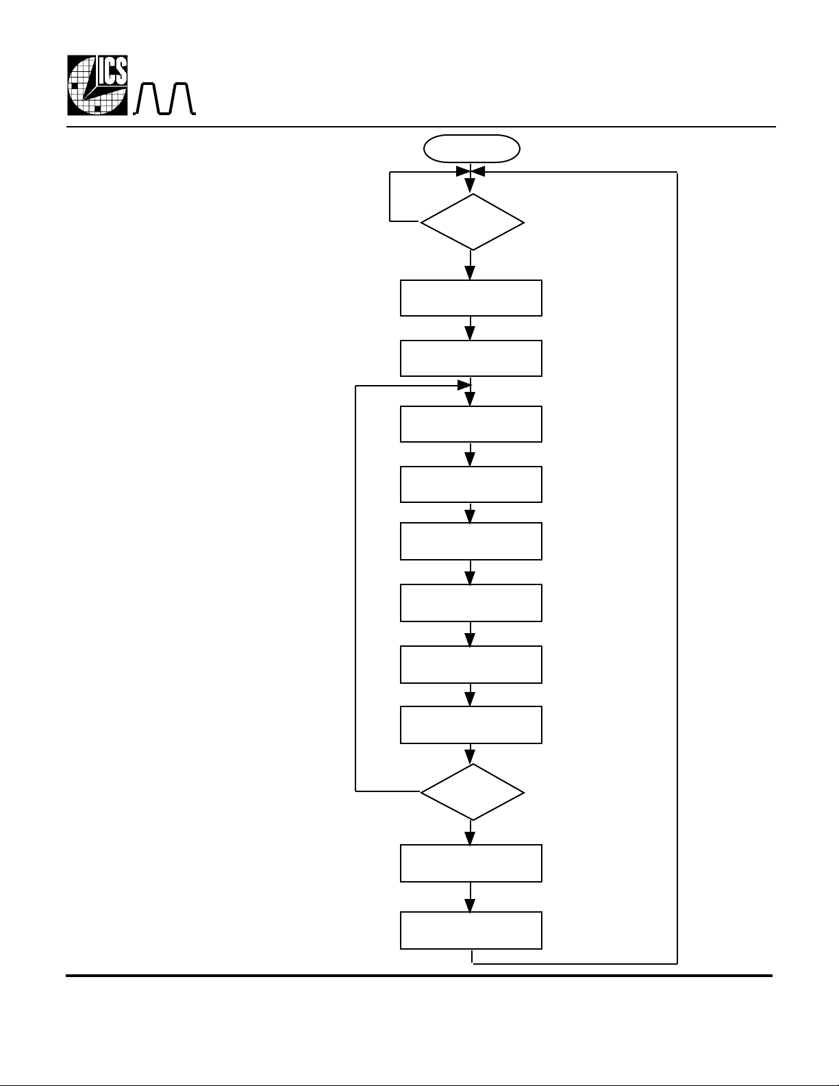
IC Operation
(Periodic Conversions Enabled)
Power ON
Is
Screen
N
Touched?
Y
Write D4, D5 Reg 0 And
D2, D3 Reg 1 To 1
Issue Interrupt
(If Enabled)
Convert
Y Co-Ordinates
Store Y Co-Ordinates In
Reg 4 and Reg 5
Touch Screen Controller
Convert
X Co-Ordinates
Store X Co-Ordinates in
Reg 2 and Reg 3
Write D7 Reg 0 To 1
Issue Interrupt
(If Enabled)
Is
Screen
Y
Touched?
N
Write D4, D5 Reg 0 And
D2, D3 Reg 1 To 0
Issue Interrupt
(if Enabled)
MDS 712 I 3 Revision 100899 Printed 11/16/00
Integrated Circuit Systems, Inc.•525 Race St.•San Jose•CA•95126•(408)295-9800tel•www.icst.com
Page 4
MK712
ICRO
C
LOCK
Touch Screen Controller
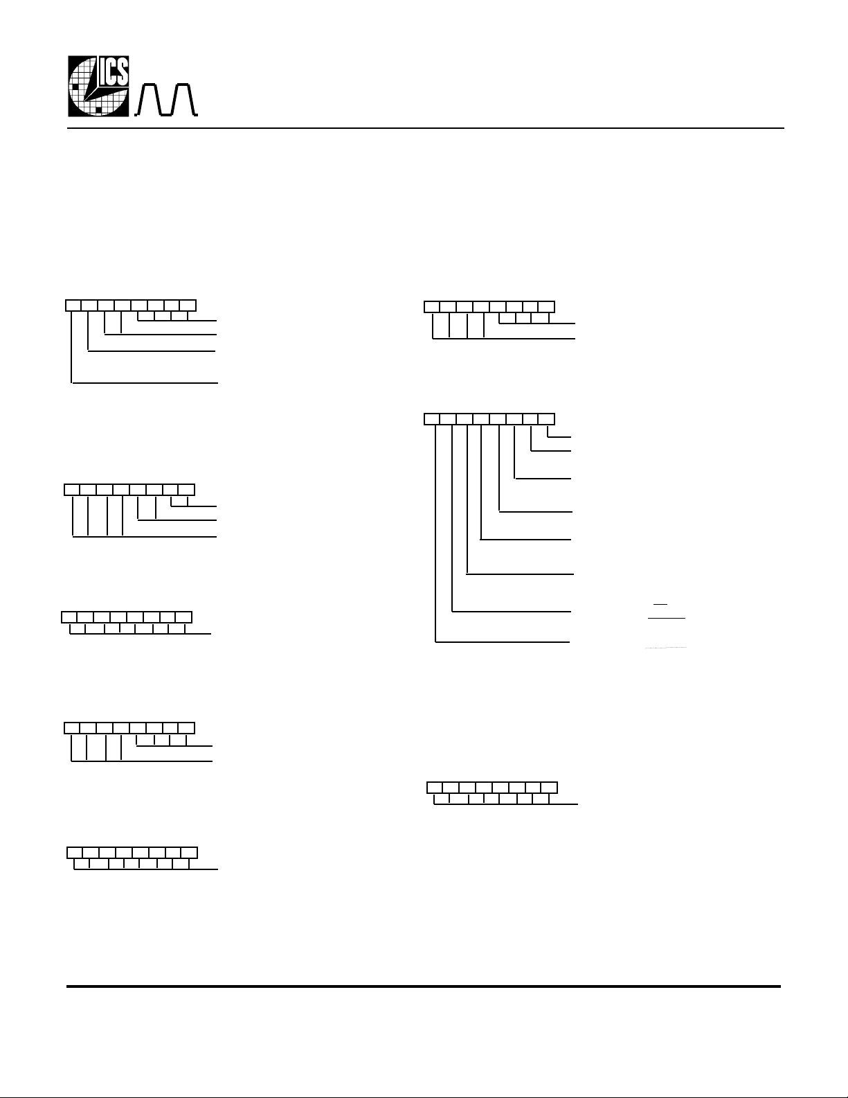
Register Description
The MK712 register set is designed to be compatible with the Gazelle pen digitizer registers allowing a
software driver for the Gazelle digitizer to be used with the MicroClock MK712. The eight 8-bit registers
are defined below:
STATUS LOW (0 READ)
7 1 03 25 46
Always zero
1 = touch
Always zero
1 = conversion complete,
cleared on Y-HIGH read
NOTE: When the screen is touched bits 4 and 5,
register 0, and bits 2 and 3 of register 1 are all set to one.
STATUS HIGH (1 READ)
7 1 03 25 46
Always zero
1 = touch
Always zero
X-LOW (2 READ)
7 1 03 25 46
Low order bits of X co-ordinate
X-HIGH (3 READ)
7 1 03 25 46
High order bits of X co-ordinate
Always zero
Y-LOW (4 READ)
7 1 03 25 46
Low order bits of Y co-ordinate
Y-HIGH (5 READ)
7 1 03 25 46
High order bits of Y co-ordinate
Always zero
CONTROL (6 R/W)
7 1 03 25 46
1 = enable interrupts
1 = interrupt on conversion
complete ( if bit 0 = 1)
1 = interrupt on change in
touch status (if bit 0 = 1)
1 = interrupt on change in
touch status (if bit 0 = 1)
1 = enable periodic conversions at
rate indicated by RATE register
1 = read one point. Cleared when
conversion complete. Only functions
when bit 4 = 0
0 = powerdown (PD). Conversions,
interrupts and TOUCH output disabled
1 = powerdown (PD). Conversions,
interrupts and TOUCH output
disabled.
NOTE: Bits 2 or 3 and bits 6 or 7 are logically OR’d. For
example writing bit 2 or bit 3 to a one will enable interrupts
on change in touch status.
RATE (7 R/W)
7 1 03 25 46
Count controls frequency of
conversion when periodic
conversions are enabled. See
table on page 5.
MDS 712 I 4 Revision 100899 Printed 11/16/00
Integrated Circuit Systems, Inc.•525 Race St.•San Jose•CA•95126•(408)295-9800tel•www.icst.com
Page 5
MK712
ICRO
C
LOCK
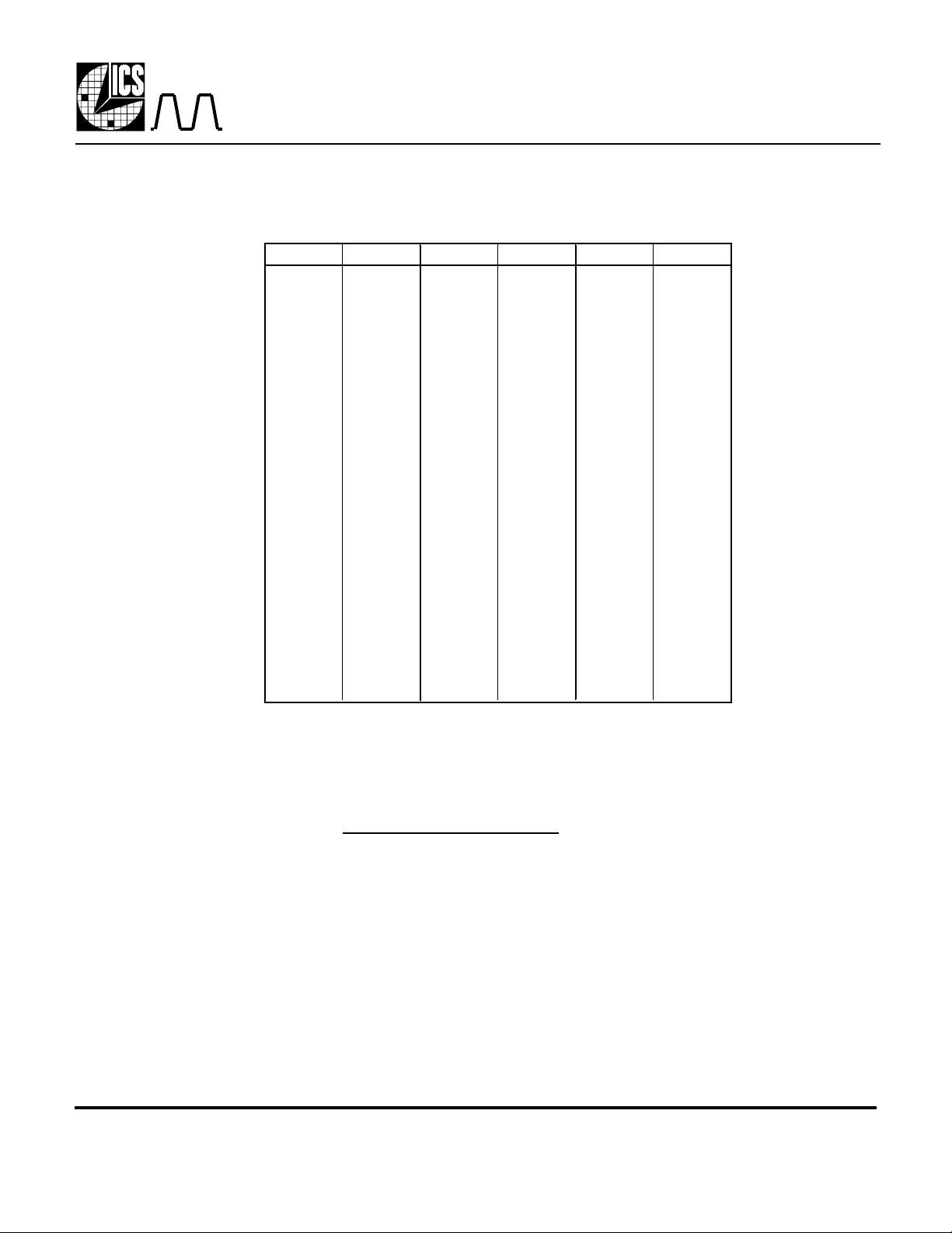
Rate Register (Register 7) Programming
Count P.P.S. Count P.P.S. Count P.P.S.
0 to 8
10 187 30 90 110 29
11 177 31 88 115 28
12 169 32 86 120 27
13 161 33 84 125 26
14 154 34 82 130 25
15 147 35 80 135 24
16 141 40 72 140 24
17 136 45 65 145 23
18 131 50 60 150 22
19 126 55 55 155 21
20 122 60 51 165 20
21 118 65 47 175 19
22 114 70 44 185 18
23 110 75 42 195 17
24 107 80 39 205 16
25 104 85 37 225 15
26 101 90 35 235 14
27 98 95 34 255 13
Not Permitted
9 197 29 93 105 31
Touch Screen Controller
28 95 100 32
P.P.S. = Points Per Second. With a 14.318 MHz clock.
Calculating Points Per Second
The formula for determining P.P.S. is:
fin
P.P.S. =
35716 + (4096 x COUNT)
Where fin is the frequency
of the CLKIN input.
Power-On Reset
On application of power, an internal reset is generated that clears all bits in registers 0, 1, and 6. Register 7 is
set to 32 giving a rate of 86 PPS. Note that clearing register 6 puts the IC into the power down condition.
Initializing the MK712
The interrupt on the MK712 can only be cleared by reading a register or by writing register 6 to the
power down condition. After a fault condition, initialize the MK712 by writing register 6 to zero and
then writing register 6 to the desired value. This will always clear pending interrupts.
MDS 712 I 5 Revision 100899 Printed 11/16/00
Integrated Circuit Systems, Inc.•525 Race St.•San Jose•CA•95126•(408)295-9800tel•www.icst.com
Page 6

MK712
ICRO
Recommended Circuit
From
Microprocessor
14.318 MHz
+3.3V or +5V
22µF
0.1µF
C
0.1µF
LOCK
RD
CS
WR
A0 - A2
D0 - D7
CLKIN
VDD
VDD
VDD
GND
GND
GND
TOUCH
INT
XH
XL
YH
YL
Touch Screen Controller
To Power Management
To Interrupt Controller
X HIGH
To
Touch
Screen
0.1µF
X LOW
Y HIGH
Y LOW
0.1µF0.01µF 0.01µF
Pen Bounce
When the screen is untouched, the Y plate is driven high and the X plate is driven low. When the screen is
touched, the X plate is pulled high, which is detected by the MK712. This initiates a conversion (as long as
periodic conversions are enabled). Some de-bounce is provided by the time constant of the screen
decoupling capacitors combined with the screen resistance. However, once conversions have started, pen
bounce will not be detected until after both the X and Y points have been taken.
If the pen is lifted during a conversion, this will also not be detected until the conversion is complete. This is
typically indicated by a point with the correct Y coordinates, but minimum (for that screen) X coordinates.
Screen Decoupling
The component values suggested should give excellent results. However, for screens with a high
resistance operating at a high conversion rate, extra interrupts may be issued. This is because the time
constant of the screen decoupling capacitors and screen resistance is high, resulting in the screen
appearing to be untouched and then touched between conversions. These extra interrupts can be
eliminated by reducing the size of the screen decoupling capacitors on pins XH, XL, YH, and YL.
This will, however, slightly reduce the noise rejection, which could decrease the accuracy of the
conversion.
MDS 712 I 6 Revision 100899 Printed 11/16/00
Integrated Circuit Systems, Inc.•525 Race St.•San Jose•CA•95126•(408)295-9800tel•www.icst.com
Page 7

MK712
ICRO
C
LOCK
Touch Screen Controller
Optimizing Performance when Reading and Writing Registers
Reading and writing the MK712 generates digital noise that may reduce the accuracy of the A to D
converter. This noise has several causes, including board layout, data bus loading, and power supply
voltage. By appropriately timing the register operations, the effects of this noise can be minimized.
After an interrupt is issued, the MK712 allows a minimum of 1 millisecond to elapse before
initiating the conversion cycle. This allows the screen drivers to settle. For best performance,
complete all register operations within this 1ms window after an interrupt.
Power Down/Stopping the Clock
If the screen is untouched, the supply current is under 3µA. If the input clock is stopped, the supply
current is also less than 3µA. When the screen is touched with no clock, TOUCH goes low and INT
goes high, but no further operations occur until the clock starts. A to D conversions are invalid until
after the clock has stabilized at the correct frequency and one full conversion cycle has been
completed.
Input Clock
The MK712 is highly tolerant of different clock frequencies (from 12 to 20 MHz), rise times, and
duty cycles. However, any input clock undershoot or overshoot will cause the MK712 to draw extra
current. This can be eliminated by using a MicroClock clock synthesizer and properly terminating
the clock driver. MicroClock makes low power clock synthesizers with 14.3 MHz power down.
Resistive Touch Screen (4 Wire)
Resistive touch screens consist of 2 resistive plates that are separated by a small gap. Each plate has an
electrode at each end and when the screen is touched, the two plates are shorted together at that point.
YH
Y PLATE
X PLATE
Electrode
XL
YL
If a voltage is applied, for example, between XL and XH, then a voltage divider is formed on the X
PLATE. When the Y PLATE is touched to the X PLATE, a voltage will be developed on the Y PLATE
that is proportional to distance of the touch from XL and XH. By accurately measuring this voltage, the
position of the touch can be determined.
XH
MDS 712 I 7 Revision 100899 Printed 11/16/00
Integrated Circuit Systems, Inc.•525 Race St.•San Jose•CA•95126•(408)295-9800tel•www.icst.com
Page 8

MK712
ICRO
C
LOCK
Touch Screen Controller
Recommended Method for Reading Points
If the user is pressing lightly on the touch screen, it is likely that the screen contact will be intermittent.
The screen will bounce, causing false points. This effect can be reduced by insuring that the screen is
touched both before and after a conversion. By doing this, the first and last point in a series of points
are discarded. The following algorithm checks that a point has valid touches both before and after a
conversion, and it distinguishes between change-in-touch interrupts and conversion complete
interrupts. Register 6 bits 0, 1, and 2 must all be true (logical 1) in order to use this method.
Start
Wait for Interrupt
Interrupt
Increment
n
Read Register 0 D7D5, store as D7D5(n)
No
Is D7D5(n-1) = 11b
and D7D5(n) =11b?
Yes
Write point n-1 to display
Read X and Y, store as point n
Are this point and the previous point valid?
(11b = binary 11)
Write previous point.
Warning - When Using a Switching Regulator Power Supply
When using the MK712 in a system where the power is supplied by a switching regulator, do not
perform screen conversions when the regulator is operating in the power saving mode. Some switching
regulators feature a low power mode (for example, Linear Technology’s “Burst Mode”) where the
output is turned on and off in order to save power. The extra power supply noise generated when using
this mode causes spurious data points to be returned from the MK712, so it should be disabled when
the MK712 is doing screen conversions.
MDS 712 I 8 Revision 100899 Printed 11/16/00
Integrated Circuit Systems, Inc.•525 Race St.•San Jose•CA•95126•(408)295-9800tel•www.icst.com
Page 9

MK712
ICRO
C
LOCK
Touch Screen Controller
Analog to Digital Converter Operation
The 12-bit ADC converts X and Y co-ordinates at a rate determined by registers 6 and 7. The
converter uses a ratiometric technique to give absolute co-ordinates on the screen, largely independent
of variations in screen resistance, temperature or power supply voltage. The total voltage applied across
the screen is defined as full-scale for the converter (i.e. 4095) and any point touched on the screen is
proportional to this. For example, if the screen is touched exactly in the center, the converter will read
2047. This feature may allow for the elimination of calibration upon startup.
However, the full scale voltage is defined at the IC pins and so any parasitic interconnect resistance will
be included in full scale. In addition, the interconnect resistances on the screen also account for about
20% of the total resistance. This means that approximately the bottom 10% and top 10% of full scale
are inaccessible.
The converter is guaranteed to be monotonic, with no missing codes.
BOARD AND WIRE
INTERCONNECT
MK712
XH
YL
XL
FULL
SCALE
(4095)
SCREEN
INTERCONNECT
SCREEN
X
CO-ORDINATE
SCREEN
INTERCONNECT
BOARD AND WIRE
INTERCONNECT
MDS 712 I 9 Revision 100899 Printed 11/16/00
Integrated Circuit Systems, Inc.•525 Race St.•San Jose•CA•95126•(408)295-9800tel•www.icst.com
Page 10

MK712
exposure to levels above the operating limits but below the Absolute Maximums may affect device reliability.
2. Consult MicroClock about the best device to use to generate the input clock.
3. With no missing codes.
4. Assumes no 14.3MHz input clock overshoot, 300 Ω screen, 100 PPS
5. Assumes no 14.3MHz input clock overshoot, no touch
6. With no touch, no clock
ABSOLUTE MAXIMUM RATINGS (note 1)
ICRO
C
LOCK
Touch Screen Controller
Electrical Specifications
Parameter Conditions Minimum Typical Maximum Units
Supply voltage, VDD Referenced to GND 7 V
Inputs and Clock Outputs Referenced to GND -0.5 VDD+0.5 V
Ambient Operating Temperature 0 70 °C
Soldering Temperature Max of 20 seconds 260 °C
Storage temperature -65 150 °C
DC CHARACTERISTICS
Operating Voltage, VDD 3.0 5.5 V
Input High Voltage, VIH VDD=5V 2.0 V
Input Low Voltage, VIL VDD=5V 0.8 V
Output High Voltage, VOH IOH=-2mA VDD-0.4 V
Output High Voltage, VOH VDD=5V, IOH=-12mA 2.4 V
Output Low Voltage, VOL VDD=5V, IOL=12mA 0.4 V
Input High Voltage, VIH VDD=3.3V 1.9 V
Input Low Voltage, VIL VDD=3.3V 0.4 V
Output High Voltage, VOH VDD=3.3V, IOH=-6mA 2.4 V
Output Low Voltage, VOL VDD=3.3V, IOL=6mA 0.4 V
Operating Supply Current, IDD, at VDD=5V 300 Ω screen, 100 PPS 5 mA
Operating Supply Current, IDD, at VDD=3.3V note 4 3 mA
Operating Supply Current, IDD standby, clock note 5 0.5 3 µA
Operating Supply Current, IDD standby note 6 0.5 3 µA
Operating Supply Current, IDD power down PD=0 or PD=1, no clock 0.2 3 µA
Short Circuit Current Each output ±50 mA
Input Capacitance 7 pF
AC CHARACTERISTICS
Input Clock Frequency, pin 18 Note 2 12 14.32 20 MHz
Input Clock Duty Cycle, pin 18 at 1.5V 25 75 %
Output Rise Time 0.8 to 2.0V, VDD=5V 3 ns
Output Fall Time 2.0 to 0.8V, VDD=5V 3 ns
Resolution 12 bits
Non-linearity Monotonic, note 3 ±2 LSB
Touch Screen Resistance 100 2000 Ω
Notes: 1. Stresses beyond those listed under Absolute Maximum Ratings could cause permanent damage to the device. Prolonged
MDS 712 I 10 Revision 100899 Printed 11/16/00
Integrated Circuit Systems, Inc.•525 Race St.•San Jose•CA•95126•(408)295-9800tel•www.icst.com
Page 11

MK712
READ AND WRITE CYCLES
READ CYCLE ONLY
WRITE CYCLE ONLY
ICRO
C
LOCK
Touch Screen Controller
Register Interface Timing
# Symbol Description Min Max Unit Note
READ AND WRITE CYCLES
1 TRASC Address Setup to CS Low 5 ns
2 TRAHC Address Hold from CS High 0 ns
3 TRCCY CS High to CS Low 40 ns
READ CYCLE ONLY
4 TRSCR CS Low to RD Low 10 ns
5 TRRD RD Pulse Width 40 ns
6 TRCHR1 RD High to CS High 0 ns
7 TRCHR2 RD High to CS Low 40 ns
8 TRDC CS Low to Data 35 ns
9 TRDR RD Low to Data 35 ns
10 TRDHC CS High to Data Release 2 20 ns 1
11 TRDHR RD High to Data Release 2 20 ns 1
WRITE CYCLE ONLY
12 TRCSW CS Low to WR Low 10 ns
13 TRWR WR Pulse Width 40 ns
14 TRCHW WR High to CS High 0 ns 2
15 TRWH WR High to CS Low 40 ns
16 TRWCY WR High to WR Low 40 ns
17 TRDW Data Setup to WR High 15 ns 3
18 TRDHW Data Hold from WR High 15 ns 4
19 TRDWC Data Setup to CS High 15 ns 3
20 TRDHWC Data Hold from CS High 15 ns 4
Notes: 1. RD edges may precede or follow CS edges.
2. WR edges may precede or follow CS edges.
3. Either TRDW or TRDWC specification must be met.
4. Either TRDHW or TRDHWC specification must be met.
5. It is not permitted to have both RD and WR low at the same time.
MDS 712 I 11 Revision 100899 Printed 11/16/00
Integrated Circuit Systems, Inc.•525 Race St.•San Jose•CA•95126•(408)295-9800tel•www.icst.com
Page 12

MK712
Register Read
A0 - A2
CS
RD
D0 - D7
Register Write
ICRO
1
C
4
8
LOCK
5
9
Touch Screen Controller
2
3
6
7
10
11
A0 - A2
CS
WR
D0 - D7
1 2
12 13
19
14
1817
20
3
15
16
MDS 712 I 12 Revision 100899 Printed 11/16/00
Integrated Circuit Systems, Inc.•525 Race St.•San Jose•CA•95126•(408)295-9800tel•www.icst.com
Page 13

MK712
IDD
(mA)
Touch Screen Controller
12
ICRO
C
LOCK
MK712 Power Supply Current vs. Touchscreen Resistance
10
8
6
4
2
0
100 1000 10000
Touchscreen Resistance (Ω)
VDD=3.3V
197 points per second
147 points per second
86 points per second
13 points per second
Graph 1
IDD
(mA)
18
16
MK712 Power Supply Current vs. Touchscreen Resistance
VDD=5V
14
12
10
8
6
4
2
0
100 1000 10000
MK712 Power Supply Current vs. Touchscreen Resistance
Vdd= 5 V
197 points per second
147 points per second
86 points per second
13 points per second
Touchscreen Resistance (Ω)
Graph 2
MDS 712 I 13 Revision 100899 Printed 11/16/00
Integrated Circuit Systems, Inc.•525 Race St.•San Jose•CA•95126•(408)295-9800tel•www.icst.com
Page 14

MK712
IDD
(mA)
ICRO
9
8
7
6
5
4
3
2
1
0
0 50 100 150 200
C
LOCK
MK712 Power Supply Current vs. Conversion Rate
Screen Resistance = 320Ω
Conversion Rate (Points Per Second)
Touch Screen Controller
VDD=5V
VDD=3.3V
Graph 3
MDS 712 I 14 Revision 100899 Printed 11/16/00
Integrated Circuit Systems, Inc.•525 Race St.•San Jose•CA•95126•(408)295-9800tel•www.icst.com
Page 15

MK712
Suggested Layout
0.01µF
To
Touch
Screen
0.1µF
ICRO
22µF
G
0.1µF
C
LOCK
0.1µF
0.01µF
V
G
Pin 1
2
3
4
5
6
7
8
9
10
11
12
13
14
Touch Screen Controller
28
27
26
25
24
23
22
21
20
19
18
17
16
15
G
0.1µF
V
G = connection to ground plane
= connection to VDD plane
V
Notes:
1. The 14.318 MHz input clock on pin 18 should have a 33Ω series termination resistor at its source.
Consult MicroClock for the best way to generate this clock.
2. All digital signals should be kept well away from pins 4, 5, 6, 7, 8, 9, 10, and 11, and any traces
connected to those pins.
MDS 712 I 15 Revision 100899 Printed 11/16/00
Integrated Circuit Systems, Inc.•525 Race St.•San Jose•CA•95126•(408)295-9800tel•www.icst.com
Page 16

MK712
Inches
Millimeters
Millimeters
ICRO
C
LOCK
Package Outline and Package Dimensions
E H
h x 45°
D
Q
e
b
c
Ordering Information
Touch Screen Controller
28 pin SOIC wide
Symbol Min Max Min Max
A 0.092 0.104 2.3368 2.6416
b 0.014 0.019 0.356 0.483
c 0.009 0.012 0.229 0.305
D 0.696 0.712 17.678 18.085
E 0.290 0.300 7.366 7.620
H 0.394 0.419 10.008 10.643
e
h 0.016 0.406
Q 0.003 0.011 0.076 0.279
28 pin SSOP (QSOP)
Symbol Min Max
A 1.55 1.73
A
b 0.203 0.305
c 0.190 0.254
D 9.780 10.160
E 3.810 4.064
H 5.840 6.223
e
h 0.410
Q 0.127 0.254
Part/Order Number Marking Package Temperature
MK712S MK712S 28 pin SOIC 0 to +70°C
MK712STR MK712S Add tape and reel 0 to +70°C
MK712SI MK712SI 28 pin SOIC -30 to +70°C
MK712SITR MK712SI Add tape and reel -30 to +70°C
MK712R MK712R 28 pin SSOP 0 to +70°C
MK712RTR MK712R Add tape and reel 0 to +70°C
MK712RI MK712RI 28 pin SSOP -30 to +70°C
MK712RITR MK712RI Add tape and reel -30 to +70°C
While the information presented herein has been checked for both accuracy and reliability, Integrated Circuit Systems, Incorporated (ICS) assumes no responsibility for either its
use or for the infringement of any patents or other rights of third parties, which would result from its use. No other circuits, patents, or licenses are implied. This product is
intended for use in normal commercial applications. Any other applications such as those requiring special processing, high reliability, or other extraordinary environmental
requirements are not recommended without additional processing by ICS. ICS reserves the right to change any circuitry or specifications without notice. ICS does not authorize or
warrant any ICS product for use in life support devices or critical medical instruments.
©1995 ICS/MicroClock
MDS 712 I 16 Revision 100899 Printed 11/16/00
Integrated Circuit Systems, Inc.•525 Race St.•San Jose•CA•95126•(408)295-9800tel•www.icst.com
 Loading...