

Page 1
.COMPATIBLEWITH MK68000 CPU
.COMPATIBLEWITH MK68000 SERIESDMA’s
.TWO INDEPENDENT FULL-DUPLEX CHAN-
NELS
.TWO INDEPENDENT BAUD-RATE GENER-
ATORS
Crystaloscillator input
-
Single-phase TTL clockinput
-
.DIRECTLYADDRESSABLE REGISTERS
(all control registers are read/write)
.DATA RATE IN SYNCHRONOUS OR ASYN-
CHRONOUSMODES
0-1.25M bits/second with 5.0MHz system
-
clockrate
.SELF-TEST CAPABILITY
.RECEIVE DATA REGISTERS ARE QUADRU-
PLY BUFFERED ; TRANSMIT REGISTERS
ARE DOUBLY BUFFERED
.DAISY-CHAIN PRIORITY INTERRUPT LOGIC
PROVIDESAUTOMATICINTERRUPTVECTORINGWITHOUT EXTERNAL LOGIC
.MODEM STATUSCAN BE MONITORED
Separate modem controls for each channel
-
.ASYNCHRONOUS FEATURES
5, 6, 7, or 8 bits/character
-
1, 11/2,or 2 stop bits
-
Even, odd, or no parity
-
x1, x16,x32, and x64 clock modes
-
Break generation and detection
-
Parity, overrun, and framingerror detection
-
.BYTE SYNCHRONOUS FEATURES
Internal or external character synchronization
-
Oneor twosynccharacters in separate regis-
-
ters
Automatic sync character insertion
-
CDC-16or CRC-CCITT block check genera-
-
tion and checking
.BIT SYNCHRONOUSFEATURES
Abortsequence generation and detection
-
Automatic zero insertion and deletion
-
Automatic flag insertion between messages
-
Address fieldrecognition
-
I-fieldresidue handling
-
Validreceivemessages protected from over-
-
run
CRC-16or CRC-CCITT block check genera-
-
tion and checking
MK68 56 4
SERIAL INPUTOUTPUT
1
PDIP48
(Plastic Package)
PLCC52
(ChipCarrier)
DESC RIPTION
The MK68564 SIO (Serial Input Output) is a dualchannel, multi-function peripheral circuit, designed
to satisfy a wide variety of serialdata communications requirements in microcomputer systems. Its
basicfunctionisa serial-to-parallel, parallel-to-serial
converter/controller ; however within that role, it is
systemssoftware configurable sothat its ”personality” may be optimized for any given serial data
communications application.
The MK68564 iscapable ofhandling asynchronous
protocols, synchronous byte-oriented protocols
(suchasIBM Bisync), and synchronous bit-oriented
protocols (such asHDLCand IBM SDLC).This versatile device can also be used to support virtually
any serial protocol for applications other than data
communications (cassette or floppy disk interface,
for example).
The MK68564cangenerateand check CRC codes
inany synchronous mode andmay beprogrammed
tocheckdata integrityin variousmodes. Thedevice
also hasfacilities for modem controlsin eachchannel. In applications where these controls are not
needed,the modemcontrolsmaybe used forgeneral-purpose I/O.
January1989
1/46
Page 2

MK 68564
SIO PIN DESCRIPTION
GND : Ground
V
: + 5 Volts (± 5%)
CC
CS : Chip Select (input, active low). CS is used to select the MK68564 SIO for accesses to
the internal registers. CS and IACK must not be asserted at the same time.
R/W : Read/write (input). R/W is the signal from the bus master, indicating wether the current
bus cycle is a Read (high) or Write (low) cycle.
DTACK : Data Transfer Acknowledge (output, active low, three stateable). DTACK is used to
signal the bus master that data is ready or that data has been accepted by the
MK68564 SIO.
A1-A5 : Address Bus (inputs). The address bus is used to select one of the internal registers
during a read or write cycle.
D0-D7 Data Bus (bidirectional, threee-stateable). The data bus is used to transfer data to or
from the internal registers during a read or write cycle. It is also used to pass a vector
during an interrupt acknowledge cycle.
CLK : Clock (input). This input is used to provide the internal timing for the MK68564 SIO.
RESET : Device Reset (input, active low). RESET disables both receivers and transmitters, forces
TxDA and TxDB to a marking condition, forces the modem controls high and disables
all interrupts. With the exception of the status registers, data registers, and the vector
register, all internal registers are cleared. The vector register is reset to ”0FH”.
INTR : Interrupt Request (output, active low, open drain). INTR is asserted when the MK68564
SIO is requesting an interrupt. INTR is negated during an interrupt acknowledge cycle
or by clearing the pending interrupt(s) through software.
IACK : Interrupt acknowledge (input, active low). IACK is used to signal the MK68564 SIO that
the CPU is acknowledging an interrupt. CS and IACK must not be asserted at the same
time.
IEI : Interrupt Enable In (input, active low). IEI is used to signal the MK68564 SIO that no
higher priority device is requesting interrupt service.
IEO : Interrupt Enable Out (output, active low). IEO is used to signal lower priority peripherals
that neither the MK68564 SIO nor another higher priority peripheral is requesting
interrupt service.
XTAL1, XTAL2 : Baud Rate Generator inputs. A crystal may be connected between XTAL1 and XTAL2,
or XTAL1 may be driven with a TTL level clock. When using a crystal, external
capacitors must be connectd. When driving XTAL1 with a TTL level clock, XTAL2 must
be allowed to float.
RxRDYA, RxRDYB: Receiver Ready (outputs, active low). Programmable DMA output for the receiver. The
RxRDY pins pulse low when a character is available in the receive buffer.
TxRDYA, TxRDYB : Transmitter Ready (outputs, active low). Programmable DMA output for the transmitter.
The TxRDY pins pulse low when the transmit buffer is empty.
CTSA, CTSB : Clear to Send (inputs, active low). If Tx Auto Enables is selected, these inputs enable
the transmitter of their respective channels. If Tx Auto Enables is not selected, these
inputs may be used as general purpose input pins. The inputs are Scmit-trigger
buffered to allow slow rise-time input signals.
DCDA, DCDB : Data Carrier Detect (inputs, active low). If Rx Auto Enables is selected, these inputs
enable the receiver of their respective channels. If Rx Auto Enables is not selected,
these inputs may be used as general purpose input pins. The inputs are Schmit-trigger
buffered to allow slow rise-time input signals.
RxDA, RxDB : Receive Data (inputs, active high). Serial data input to the receiver.
TxDA, TxDB : Transmit Data (outputs, active high). Serial data output of the transmitter.
2/46
Page 3
MK68564
SIO PIN DESCRIPTION (continued)
RxCA, RxCB : Receiver Clocks (input/output). Programmable pin, receive clock input, or baud rate
generator output. The inputs are Schmit-trigger buffered to allow slow rise-time input
signals.
TxCA, TxCB : Transmitter Clocks (input/output). Programmable pin, transmit clock input, or baud rate
generator output. The inputs are Schmit-trigger buffered to allow slow rise-time input
signals.
RTSA, RTSB : Request to Send (outputs, active low). These outputs follow the inverted state
programmed into the RTS bit. When the RTS bit is reset in the asynchronous mode, the
output will not change until the character in the transmitter is completely shifted out.
These pins may be used as general purpose outputs.
DTRA, DTRB : Data Terminal Ready (outputs, Active low). These outputs follow the inverted state
programmed into the DTR bit. These pins may also be used as general purpose
outputs.
SYNCA, SYNCB : Synchronization (input/output, active low). The SYNC pin is an output when Monosync,
Bisync, or SDLC mode is programmed. It is asserted when a sync/flag character is
detected by the receiver. The SYNCpin is a general purpose input in the Asynchronous
mode and an input to the receiver in the External Sync Mode.
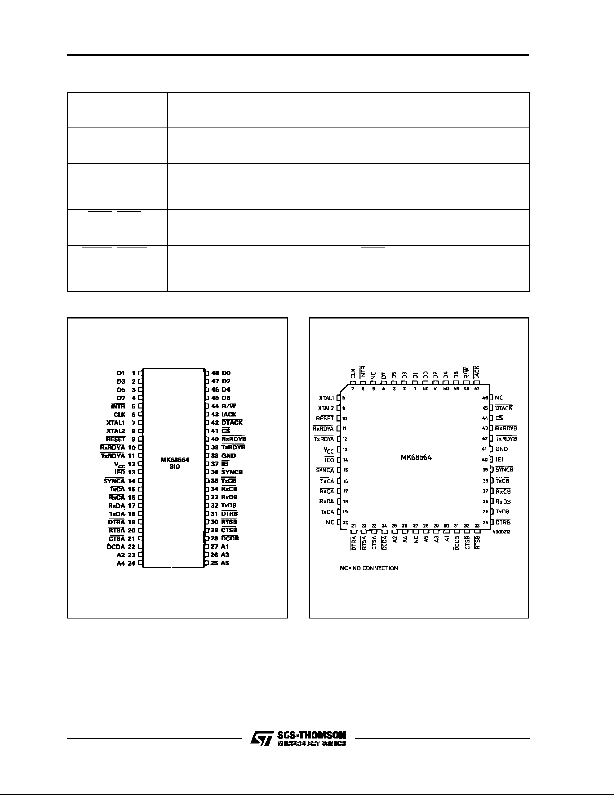
Figure 1a: DualIn Line Pin Configuration. Figure 1b : Chip Carrier Pin Configuration.
3/46
Page 4

MK 68564
SIO SYSTEM INTERFACE
INTRODUCTION
The MK68564 SIO is designed for simple and effi-
cientinterface to a MK68000 CPU system.All data
transfers between the SIOand the CPU are asynchronous tothe system clock. TheSIO system
timing is derived from thechip select input (CS)duringnormalread and write sequences, andfrom the
interrupt acknowledge input (IACK) during an exception processing sequence. CS is a function of
address decode and (normally) lower data strobe
(LDS). IACKisafunction oftheinterruptlevelon address lines A1, A2, and A3, an interrupt acknowledgefunction code(FC0-FC2), and LDS.
Note : CS and IACK can never be asserted at the
sametime.
Note: Unusedinputs should bepulled up or down,
but neverleft floating.
READSEQUENCE
TheSIOwill begin areadcycleif,on thefalling edge
of CS,the read-write (R/W) pin ishigh. The SIO will
respond by decoding the address bus (A1-A5) for
the register selected, byplacingthecontentsof that
register onthedatabuspins(D0-D7),andbydriving
the data transfer acknowledge (DTACK) pin low. If
theregisterselected is not implemented onthe SIO,
the data bus pins will be driven high, and then
DTACK will beasserted. When the CPUhas acquired the data, the CS signal is driven high,at which
time the SIOwill drive DTACK high and thenthreestateDTACK and D0-D7.
WRITESEQUENCE
TheSIOwillbegin awritecycleif, onthefalling edge
of CS, the R/W pin is low. The SIO will respondby
latchingthe data bus,by decoding the address bus
forthe register selected, by loading theregisterwith
the contents of thedata bus,and bydriving DTACK
low. When the CPU hasfinished the cycle, the CS
input is driven high. At this time, the SIO will drive
DTACKhighand will thenthree-state DTACK. If the
register selectedisnotimplemented on theSIO,the
normal write sequence will proceed, but the data
bus contents will not be stored.
INTERRUPT SEQUENCE
The SIO isdesignedto operate asan independent,
interrupting peripheral, or, when interconnected
with other components, an interrupt priority daisy
chaincan beformed.
Independent Operation. Independent operation
requires that the interrupt enable in pin (IEI) be
connected to ground. The SIO starts the interrupt
sequence bydrivingthe interrupt request pin(INTR)
low. The CPUresponds to the interrupt bystarting
an interrupt acknowledge cycle, in which the SIO
IACKpin is driven low. Thehighest priority interrupt
request intheSIO,atthetimeIACKgoeslow,places
itsvectoron thedatabuspins.TheSIOreleasesthe
INTRpinanddrivesDTACKlow.WhentheCPUhas
acquired the vector,the IACK signal is driven high.
The SIO responds bydrivingDTACK toa highlevel
and then three-stating DTACK and D0-D7. If more
than one interrupt request is pending at the start of
an interrupt acknowledge sequence, the SIO will
drive the INTR pin low following the completion of
the interrupt acknowledge cycle.This sequencewill
continue until all pending interrupts are cleared. If
the SIO is not requesting an interrupt when IACK
goeslow,the SIOwill notrespond totheIACKsignal
; DTACKand the data buswill remain three-stated.
DaisyChainOperation. Theinterrupt priority chain
is formed by connecting the interrupt enable out pin
(IEO)of a higher priority part toIEI ofthe next lower
priority part. The highest priority part in the chain
shouldhave IEI tied to ground. The Daisy Chaining
capability (figures 2 and 3) requires that all parts in
a chain have a common IACK signal. When the
commonIACK goes low,all partsfreeze and prioritize interrupts in parallel. Then priority is passed
down the chain, via IEI and IEO, until a part which
has a pending interrupt, once IEI goes low, passes
a vector, does not propagate IEO, and generates
DTACK.
The state of the IEI pin does not affect the SIO interrupt control logic.The SIOcan generate an interruptrequest any time itsinterrupts areenabled. The
IEO pin is normally high ; it will only go low during
anIACKcycleifIEIislowandnointerrupt ispending
intheSIO.TheIEO pin willbe forcedhighwhenever
IACKor IEI goes high.
4/46
Page 5
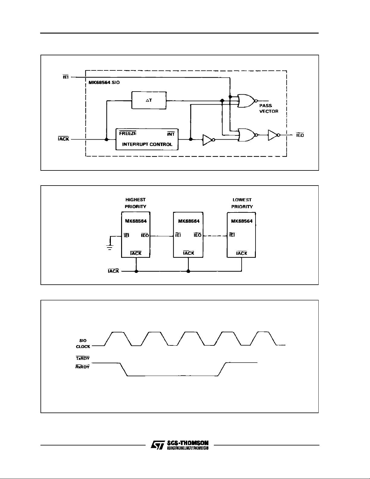
Figure 2 : Conceptual Circuit of the MK68564 SIODaisy Chaining Logic.
Figure 3 : Daisy Chaining.
MK68564
V000376
Figure 4 : DMAInterface Timing.
V000377
V000378
5/46
Page 6

MK 68564
DMA INTERFACE
The SIO isdesigned tointerface tothe68000 family
DMA’sas a 68000 compatible device, using the cycle steal mode. The SIO provides four outputs
(TxRDYA, RxRDYA, TxRDYB, RxRDYB) for requesting servicefrom theDMA.The SIOissuesarequestforservicebypulsingthe RDYpinlowfor three
clock(CLK)cycles(seefigure 4). TxRDY(when enabled) will be active when the transmit buffer becomesempty. RxRDY(whenenabled) willbe active
when a character is available in the receive buffer.
If Receive Interrupt On First Character Only is enabledduring aDMAoperation and aspecial receive
condition is detected, the RxRDY pin will not becomeactive.Instead,a special receive conditioninterrupt will be generated by the channel.
RESET
There aretwo ways of resetting theSIO : an indivi-
dual,programmable channel resetand an external
hardware reset.
The individual channel reset isgenerated by writing
”18H”to theCommandRegister forthe channel selected. All outputs associated with the channel are
resethigh,TxC and RxCareinputs, SYNCisan output,and TxDisforcedmarking.All R/W registers for
the channel areresetto ”00H”, exceptthevectorregisterand the data register, whichare not affected.
Readonlystatusregister1isresetto”01H”(AllSent
set). Break/Abort, Interrupt Pending, and Rx CharacterAvailablebitsin readonlystatus register0 are
reset ; Underrun/EOM, Hunt/Sync, and Tx Buffer
Emptyare set ; CTS andDCD bitsare setto the invertedstate oftheir respective inputpins. Any interruptspendingforthechannel arereset (anypending
interrupts inthe other channel willnot be affected).
Anexternalhardware resetoccurswhenthe RESET
pin is driven low for at least one clock (CLK) cycle.
Both channels are reset as listed above, and the
vector register is reset to ”0FH”.
ARCHITECTURE
The MK68564 SIO contains two independent, full-
duplexchannels. Eachchannel containsatransmitter, receiver, modemcontrol logic, interrupt control
logic, a baud rate generator, ten Read/Write registers,and two read only statusregisters. Eachchannelcan communicatewiththe busmasterusingpolling, interrupts, DMA, or any combination of these
threetechniques. Eachchannel also has theability
toconnect thetransmitteroutputintothereceiverwithout disturbing any external hardware.
Register Set. The register set is the heartof each
channel. A channel is configured for different
communication protocols and interface options by
programming the registers. Table 1 lists all the registersavailablein the SIOand their addresses.
Data Register. The Data Register is composed of
two separate registers : a write only register, which
is the Transmit Buffer, and a read only register,
which is the Receive Buffer. The Receive Buffer is
also the top register of a threeregister stack called
the receive dataFIFO.
Vector Register. The Vector Register is different
from the other 24 registers, because it may be accessedthrough eitherChannel A or Channel B duringa R/W cycle.During an Interrupt Acknowledge
cycle, the contentsof the Vector Register arepassedtotheCPUto beusedasapointertoaninterrupt
serviceroutine. If the StatusAffectsVectorbitisLow
in the Interrupt Control Register, any data written to
the Vector Register will bereturned unmodified duringa Read Cycleor anIACK cycle. Ifthe Status Affects Vector bit is High, the lower three bits of the
vectorreturnedduring aReadorIACKcyclearemodified to reflect the highest priority interrupt pending
in the SIO at thattime. Theupper fivebits writtento
theVector Register areunaffected. Afterahardware
reset only, this register contains a ”0FH” value,
whichistheMK68000’s uninitialized interrupt vector
assignment.
6/46
Page 7
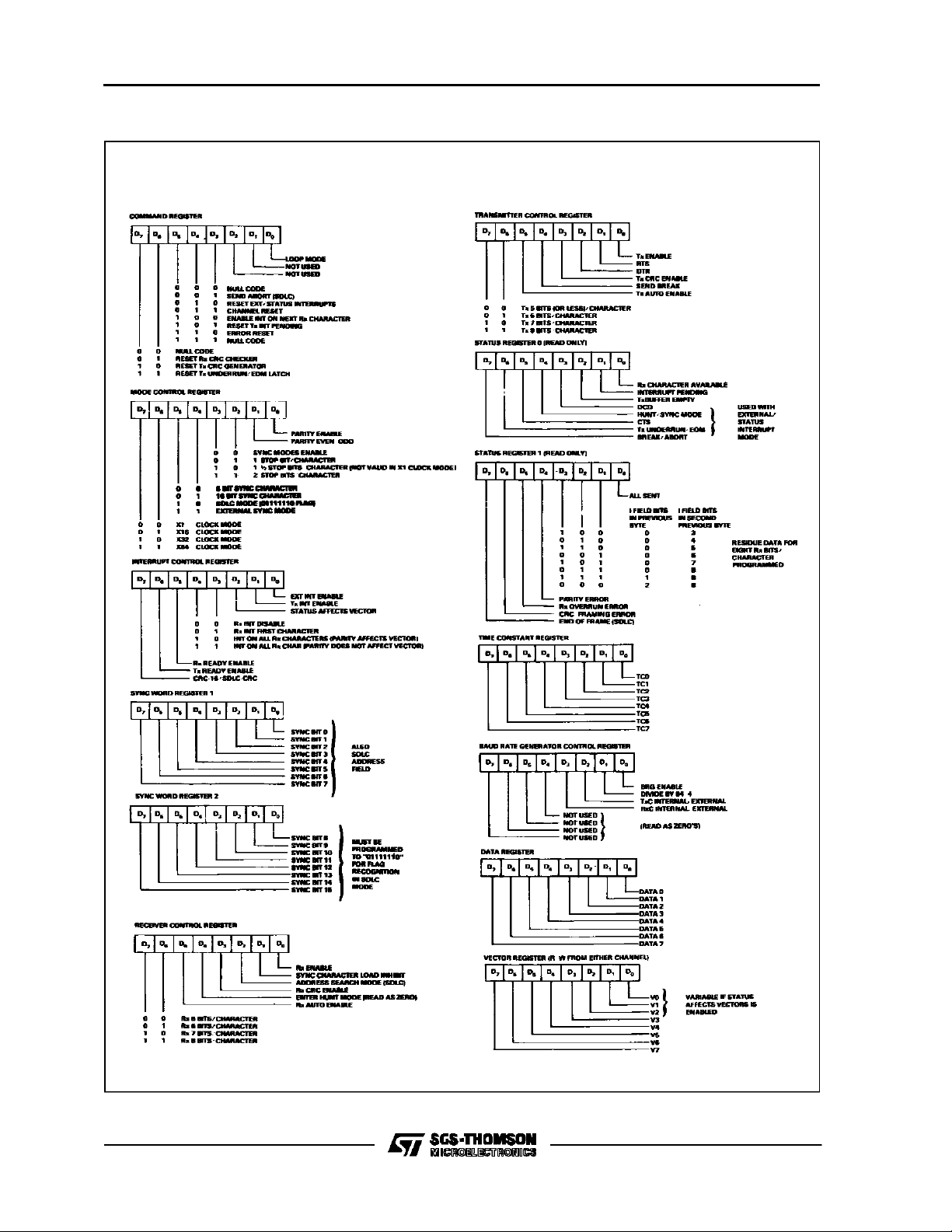
Figure 5 : Register Bit Functions.
MK68564
7/46
Page 8

MK 68564
SIO INTE RNA L REG IS TERS
The MK68564 SIOhas 25internal registers.Eachchannelhas ten R/W registers andtworeadonly registers
associatedwithit. The vectorregister maybe accessed through eitherchannel.
Table 1 : Register Map.
Address Access
54321
0
0
0
0
0
0
0
0
1
0
0
0
1
0
0
0
0
1
0
0
0
1
0
0
1
1
0
0
1
1
0
0
0
0
1
0
0
0
1
0
1
0
1
0
1
0
1
0
1
1
0
1
0
1
0
1
0
0
1
0
1
0
1
0
1
0
1
0
1
0
1
0
1
1
1
1
1
1
1
1
1
1
1
1
1
1
1
1
1
Notes : 1. Not Used,Read as ”FFH”.
2. Only One Vector Register, Accessible throughEither Channel.
0
0
1
1
1
1
1
0
0
0
0
1
0
1
0
0
1
0
1
1
1
1
1
0
0
0
0
1
0
1
0
0
1
0
1
1
1
1
1
Abbreviati o n Chan nel Regi ster Name
0
1
0
1
0
1
0
1
0
1
0
1
0
1
0
1
0
1
0
1
0
1
0
1
0
1
0
1
0
1
0
1
CMDREG
MODECTL
INTCTL
SYNC 1
SYNC 2
RCVCTL
XMTCTL
STAT 0
STAT 1
DATARG
TCREG
BRGCTL
VECTRG
CMDREG
MODECTL
INTCTL
SYNC 1
SYNC 2
RCVCTL
XMTCTL
STAT 0
STAT 1
DATARG
TCREG
BRGCTL
VECTRG
A
A
A
A
A
A
A
A
A
A
A
A
A/B
A
A
A
B
B
B
B
B
B
B
B
B
B
B
B
A/B
B
B
B
Command Register X
Mode Control Register X
Interrupt Control Register X
Sync Word Register 1 X
Sync Word Register 2 X
Receiver Control Register X
Transmitter Control Register X
Status Register 0 X
Status Register 1 X
Data Register X
Time Constant Register X
Baud Rate Generator Control Reg X
Interrupt Vector Register (note 2) X
(note 1) X
(note 1) X
(note 1) X
Read/
write
Read
Only
8/46
Page 9
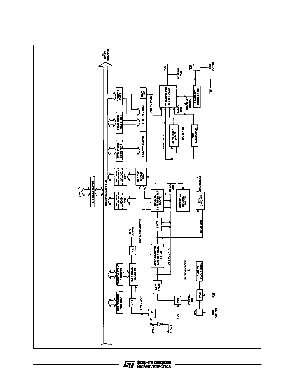
Figure 6 : Transmit and Receive Data Paths.
MK68564
V000379
9/46
Page 10

MK 68564
DATA PATH
The transmit and receivedata pathsfor each chan-
nel are shown in figure 6. The receiver has three
8-bit buffer registers in a FIFOarrangement (to provide a 3-bytedelay) in addition to the 8-bit receive
shift register. This arrangement creates additional
timefor theCPUtoserviceaninterrupt at thebeginning of ablock of high-speed data. The receiver error FIFO stores parity and framing errors and other
types of status information for each of the three
bytesin thereceive dataFIFO.ThereceiveerrorFIFO is loaded at the same time as the receive data
FIFO. The contents of the receive error are read
throughthe upper four bits in Status Register 1.
Incoming data is routed through one of several
paths,depending onthemodeandcharacterlength.
In the Asynchronous modes, serial data is entered
into the3-bitbuffer, if it hasa character lengthof seven oreight bits,or the data is entered into the 8-bit
receive shift register, if it has a length of fiveor six
bits.
In theSynchronous mode, thedata pathis determinedby thephase ofthe receive process currently in
operation. A Synchronous Receive operation begins with the receiver in the Hunt phase, during
which timethe receiver searches the incomingdata
stream for a bit pattern that matches the preprogrammed sync characters (or flags in the SDLC
mode). If the device is programmed for Monosync
Hunt, amatch is made witha single sync character
stored in Sync Word Register 2. In Bisync Hunt, a
match ismade with the dual sync characters stored
in SyncWord Registers1 and 2. In eithercase, the
incoming data passes through the receive sync register and is compared against the programmed
synccharacters in SyncWord Registers1 and 2.
In the Monosync mode, a matchbetween the sync
character programmed into Sync Word Register 2
andthe character assembled inthereceivesync registerestablishes synchronization.
In the Bysyncmode, incoming data is shiftedto the
receive shift register,while thenext eightbits of the
message are assembled in the receive sync register.The matchbetweentheassembledcharacter in
the syncregister and the programmed character in
Sync Word Register 2, and between the character
in the shift register and the programmed character
in Sync Word Register 1 establishes synchronization.Once synchronization is established,incoming
data bypassesthe receive syncregister anddirectly
entersthe 3-bit buffer.
In the SDLC mode, all incoming data passes
throughthereceivesyncregister,whichcontinuously monitors the receive data stream and performs
zero deletion when indicated. Upon receiving five
contiguous ones, the sixth bit is inspected. If the
sixth bitis a 0, it is deleted from the data stream. If
the sixth bitis a1, the seventhbit isinspected. If the
seventh bit is a 0, a Flag sequence has beenreceived ;ifthe seventh bitisa 1,an Abortsequence has
been received.
The reformatted datafrom thereceive sync register
enters the 3-bit buffer and is transferred to the receiveshift register. Note that theSDLCreceive operationalso begins in the HuntPhase, during which
timetheSIO triesto matchtheassembled character
in the receive sync register with the flag pattern in
SyncWord Register 2. Oncethe firstflag character
is recognized, all subsequent data isroutedthrough
the path described above, regardless of character
length.
Although the same CRC checker is used for both
SDLC and synchronous data, the path taken for
eachmode is different. InBisyncprotocol, the byteoriented operation requires that the CPU decide
whether or not to include the data character in the
CRC calculation. To allow the CPU ample time to
make this decision, the SIO provides an 8-bit delay
before the data enters the CRC checker. In the
SDLCmode,nodelayis provided, since CRCiscalculated onall data betweentheopening and closing
flags.
The transmitter has an 8-bittransmit data register,
which is loaded from the internalbus, and a 20-bit
transmit shift register, which can be loaded from
Sync Word Register1, Sync Word Register 2, and
the transmit data register. Sync Word Registers 1
and 2 contain sync characters in the Monosync, Bisync,orExternal Sync modes, oraddress field (one
character long) and flag, respectively, in the SDLC
mode. During Synchronous modes, information
contained in Sync WordRegisters 1 and2is loaded
intothe transmit shift registerat the beginning of the
message and, as a time filler, in the middle of the
message if a Transmit Underrun condition occurs.
InSDLCmode,theflags areloaded intothetransmit
shift register at the beginning and endof the message.
Asynchronous data in the transmit shift register is
formattedwith startandstopbits,and itisshiftedout
tothe transmit multiplexer attheselected clockrate.
Synchronous (Monosync, Bisync, or External Sync)
data isshiftedoutto the transmit multiplexer and also the CRC generator at the x1 clock rate.
SDLC/HDLC data isshiftedout throughthe zeroinsertionlogic,whichis disabled while flags are being
sent.Forallotherfields (address, control, andframe
check),a 0isinsertedfollowingfivecontiguousones
10/46
Page 11

MK68564
in the data stream. Notethat theCRC generator result (frame check) for SDLC data is also routed
throughthe zero insertion logic.
I/O CAPABILITIES
The SIOoffers the choiceof Polling, Interrupt (vec-
toredor non-vectored), and DMATransfermodesto
transfer data, status, and control information toand
from the CPUor other bus master.
Polling.The Polledmode avoids interrupts. Status
Registers 0 and1 are updated at appropriate times
for each function being performed (for example,
CRC Errorstatus valid at the end of themessage).
All theinterrupt modesof the SIO must be
disabled to operate the device in a polled environment.
While initsPollingsequence, theCPUexamines the
statuscontained inStatus Register 0foreachchannel. Thestate of the statusbits in StatusRegister0
servesas anacknowledgetothePollinquiry. Status
bitsD0andD2 indicatethata receive ortransmitdata transfer is needed. The rest of the status bitsin
StatusRegister0 indicate special statusconditions.
The receiver error condition bits in Status Register
1 donothave tobereaduntiltheRxCharacter Availablestatus bit in StatusRegister 0 isset to a one.
Interrupts. The SIO offers an elaborate interrupt
scheme to provide fast interrupt response in realtime applications. The interrupt vector points to an
interrupt serviceroutine in the memory. To service
operations inboth channels and to eliminate thenecessityof writing a statusanalysis routine (asrequiredfora polling scheme), the SIOcanmodifytheinterrupt vectorsoitpointstooneofeight interrupt serviceroutines. Thisis done underprogram control by
setting theStatus AffectsVector bit in the Interrupt
Control Register ofchannel Aorchannel B,toaone.
When thisbit isset, the interrupt vector is modified
according to the assigned priority of the various interrupting conditions.
Note: If theStatus Affects Vector bit is set in either
channel, the vector is modified for both channels.
Thisis the onlycontrolbit thatoperates inthis mannerin the SIO.
Transmit interrupts, Receive interrupts, and External/Status interrupts are the sources of interrupts.
Each interrupt source is enabled under program
controlwith Channel Ahaving a higher priority than
Channel B, and withReceiver,Transmitter, andExternal/Statusinterrupts prioritizedin thatorder within
each channel. When the Transmit interrupt is enabled, theCPU is interrupted by the transmit buffer
becoming empty. This implies that the transmitter
must have had a data character written into it so t
canbecome empty.Whenenabled, thereceiver can
interrupt the CPU in one of threeways :
Interrupt OnFirst CharacterOnly
Interrupt OnAll Receive Characters
Interrupt OnA Special Receive Condition.
Interrupt On First Character Only.This mode is
normally used to start a software Polling loop or a
DMA transfer routine using the RxRDY pin. In this
mode, the SIO generates an interrupt on the first
character received after this mode is selected and,
thereafter, only generates an interrupt if a Special
Receive Condition occurs. The Special Receive
Conditions that can causean interrupt in this mode
are: Rx OverrunError,Framing Error (in Asynchronousmodes), and EndOf Frame (in SDLCmode).
Thismode isreinitialized bytheEnable Interrupt On
Next Rx Character command.If a Special Receive
Condition interrupt occursinthis interrupt mode,the
data withthe special conditionis held inthe receive
data FIFOuntilan Error Reset Command isissued.
InterruptOnAll ReceiveCharacters. Inthismode,
an interrupt is generated whenever thereceivedata
FIFO contains a character or a Special Receive
Condition occurs. The Special Receive Conditions
thatcan cause an interrupt in thismode are : Rx Overrun Error, Framing Error (in Asynchronous
modes), End ofFrame (in SDLC mode),and Parity
Error (if selected).
Interrupt On A Special Receive Condition. The
Special Receive Condition interrupt is not,as such,
a separate interrupt mode. Before a Special ReceiveCondition can cause aninterrupt, either theInterrupt On First Character Only or Interrupt On All
Receive Characters mode must be selected. The
Special Receive Condition interrupt will modify the
receive interrupt vectorifStatusAffectsVector isenabled.The Special Receive Condition status is displayed in the upper four bits of Status Register 1.
Two of the conditions causing a special receive interrupt arelatched whentheyoccur;they are:Parity
Error and Rx Overrun Error. These statusbits may
onlybe reset byan Error Reset command. Wheneither of these conditions occur,a read of StatusRegister 1 will reflect any errorsin the currentword in
the receive buffer plus any parity or overrun errors
sincethe last Error Reset command wasissued.
External/Status Interrupts. The main function of
the External/Status interrupt is to monitor thesignal
transitions of theCTS, DCD,and SYNCpins ; however, anExternal/Status interrupt is alsocaused by
a TransmitUnderrun condition orby thedetection of
a Break (Asynchronous mode) or Abort (SDLC
mode)sequence in thereceived datastream.When
any one of the above conditions occur, the exter-
11/46
Page 12
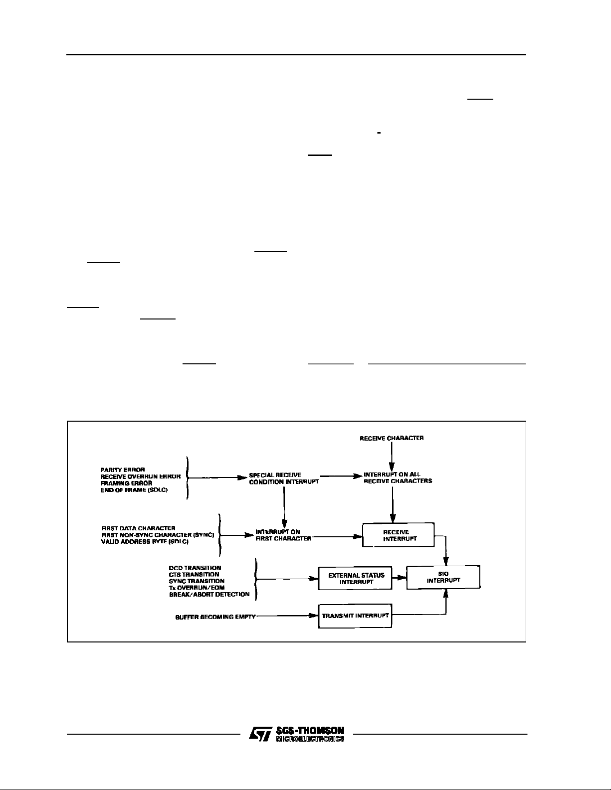
MK 68564
nal/status logiclatches thecurrent stateof allfiveinput conditions, andgenerates an interrupt. Toreinitialize the external/status logic to detect another
transition, a Reset External/Status Interrupts
command must be issued. The Break/Abort conditionallows theSIOtogenerate aninterrupt whenthe
Break/Abort sequence is detectedand terminated.
This featurefacilitates the proper termination of the
current message, correct initialization of the next
message, and the accurate timing of the Break/Abortcondition inexternal logic.
DMA Transfer
TheSIOprovides twooutput signals perchannelfor
connection to a DMA controller ; they are TxRDY
and RxRDY. The outputs are enabled under software control by writing tothe Interrupt Control Register. Both outputs willpulse Low for three system
clock cycleswhen their input conditions are active.
TxRDYwill be active whenthe Transmit Buffer
becomesempty.RxRDYwillbe activewhen acharacter isavailable in theReceive Buffer. If a Special
Receive Condition occurs when Interrupt On First
Character Only mode is selected, a receiver interrupt will be generated and RxRDY willnot become
active. This will automatically inform the CPU of a
discrepancy in the data transfer.
SELFTEST
Whenthe LoopModebit issetin theCommandRe-
gister,thereceiver shiftclockinputpin(RxC)andthe
receiver data input pin (RxD) are electrically disconnected from theinternal logic. Thetransmitdata
output pin (TxD)is connected to the internal
receiver data logic, and the transmit shift clock pin
(TxC)isconnected totheinternal receivershiftclock
logic.All other features of the SIO are unaffected.
BAUDRATE GENERATORS
Each channelin theSIO contains a programmable
baud rate generator (BRG). Each BRG consists of
an 8-bit timeconstant register, an 8-bit downcounter,a controlregister, anda flip-flop onthe output to
provide a square wave signalout. In addition tothe
flip-flopon the output, thereis alsoa flip-flop on the
inputclock;therefore, themaximum outputfrequency of theBRGisone-forth oftheinputclockfrequency. Thismaximum output frequency occurs when
divide by four mode is selected, and the time
constant register is loaded with theminimum count
of ”01H”. The equation to determine the output frequencyis :
Output
=
Input Frequency
Frequency (divideby selected)X (time constant
value in decimal)
Figure 7 : InterruptStructure.
V000380
12/46
Page 13
MK68564
Forexample,whenthe timeconstant registerisloaded with ”01H” and divide by four is selected, one
outputclock will occur for every four input clocks.If
the time constant value loaded is ”00H” (256 decimal) instead of ”01H” and divide by 64 is selected,
one output clock will occur for every 16384 input
clocks.Note that theminimum count value is”01H”
(1 decimal), and the maximum count valueis ”00H”
(256 decimal).
The output of the baud rate generator may be programmed to drive the transmitter (BRG output on
TxC),the receiver(BRGoutputon RxC), both (BRG
output on TxC and RxC), or neither(TxC and RxC
areinputs). Aftera reset, thebaud rate generator is
disabled, divide by four is selected, and TxC and
RxC are inputs.
The baudrate generator should be disabled before
the CPUwrites tothe time constantregister. Thisis
necessary because no attempt was made to synchronize the loading of anew timeconstant with the
clockused to drive the BRG.
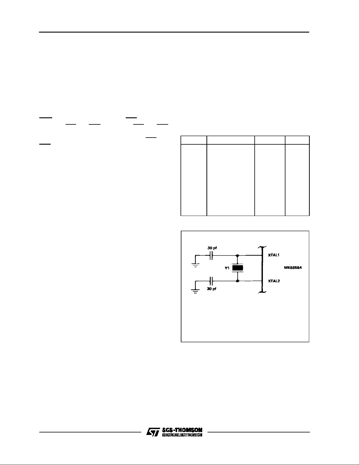
Figure 8indicates the externalcomponents needed
to connect a crystal oscillator to the SIO XTAL inputs.Theallowed crystalparameters arealsolisted.
For a 3.6864MHz input signal to the baud rate generator,thetime constants, listed in table2, areloaded to obtain the desired baud rates (in x1 clock
mode).
To set up the SIOfor Asynchronous operation, the
following registers need to be initialized : Mode
ControlRegister, Interrupt Control Register, Receiver Control Register, and Transmitter Control
Register. The Mode Control Register must be
programmed before the other registers to assure
properoperation ofthe SIO. The following registers
are used to transferdata or tocommunicate status
between the SIOand the CPU or other bus master
when operating in Asynchronous modes :
Command Register, Status Register 0, Status Register 1, DataRegister, and theVector Register.
Table 2 : Time-ConstantValues.
Ra t e Ti m e Constant Divi de By Error
19200
9600
7200
4800
3600
2400
2000
1800
1200
600
300
Figure8 :
48
96
128
192
256
24
29
32
48
96
192
SIO External Oscillator Components.
4
4
4
4
4
64
64
64
64
64
64
69 %
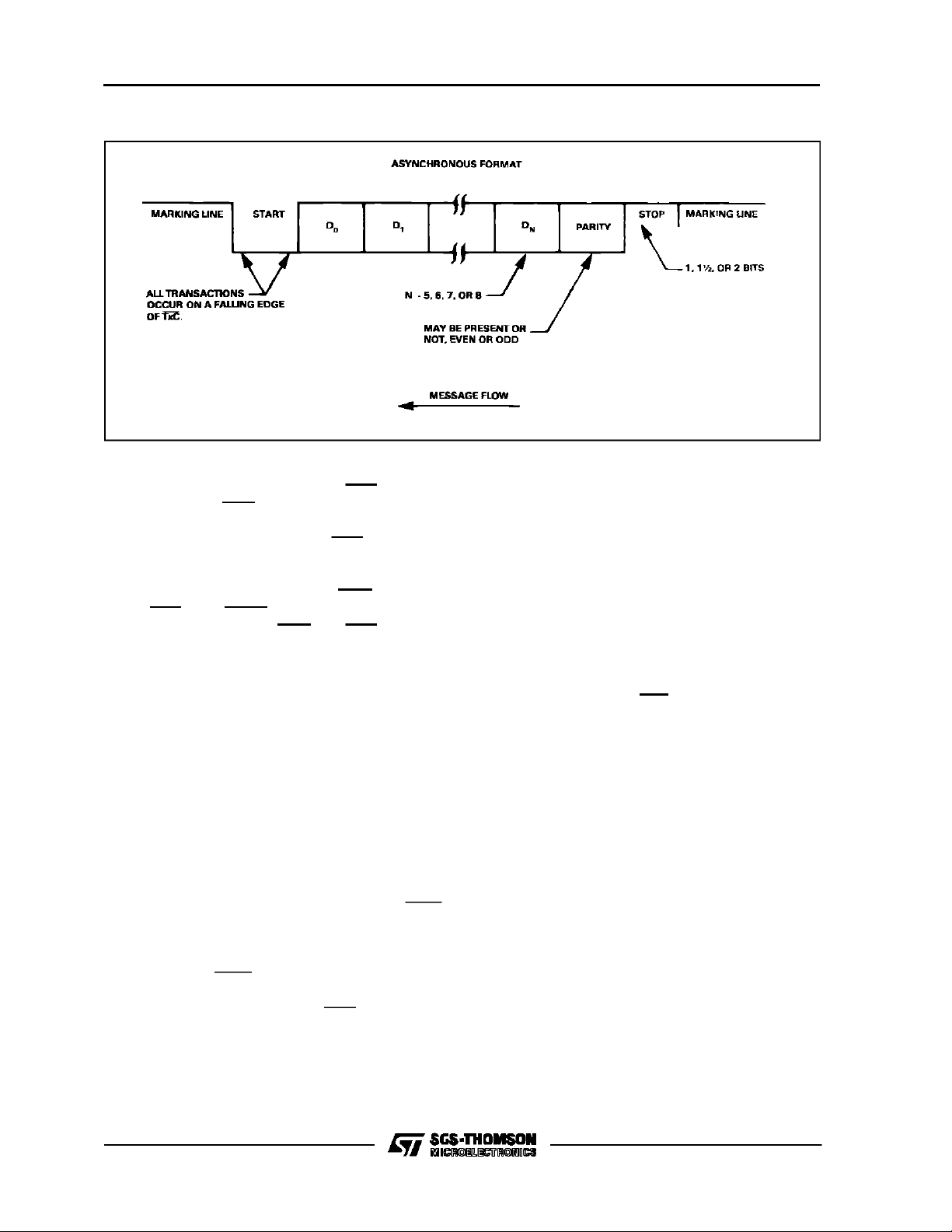
ASYNCHRO N OU S OPERAT ION
INTRODUCTION
Manytypesof Asynchronous operations are performed by the MK68564 SIO.Figure 9 represents a ty-
pical Asynchronous message format and some of
the options available on the SIO. Thetransmit processinserts start, stop, and parity bitsto a variable
data format and supplies a serialdata streamto the
Transmit Dataoutput(TxD). The receiver takesthe
data from the Receive Data input (RxD) and strips
awayexpectedstart andstop bitsat a programmed
clockrate. Itprovideserror checking foroverrun,parity, and carrier-loss errors,and, ifdesired,provides
interrupts forthese conditions.
CRYSTALPARAMETERS :
Parallel Resonance, FundamentalMode AT Cut
Rs â150Ω(Fr = 2.8- 5.0MHz)
Rs â300Ω(Fr = 2.0- 2.7MHz)
CI = 18pf ; Cm = 0.02pF ; Ch= 5pF ; Lm = 96MHz
Fr (typ)= 2.457MHz
13/46
Page 14
MK 68564
Figure 9 : Asynchronous MessageFormat.
V000382
The SIOprovides fiveI/O linesthatmay beused for
modemcontrol, forexternalinterrupts, oras general
purpose I/O.The Request To Send(RTS) and Data
Terminal Ready (DTR) pins are outputs that follow
the inverted state of their respective bits in the
Transmitter ControlRegister.The RTS pin canalso
be usedto signal theendof a message inAsynchronous modes, as explained below in the transmitter
section. The Data Carrier Detect (DCD), Clear To
Send (CTS), and SYNC pins are inputs to the SIO
in Asynchronous modes. DCD and CTS can be used as auto enablesto thereceiver and transmitter,
respectively, or if External/Status Interruptsare enabled all three input pins will be monitored for a
change ofstatus.If these inputs change fora period
of time greater than the minimum specified pulse
width,an interrupt will be generated.
In the following discussion,all interrupt modes are
assumed enabled.
ASYNCHRONOUS TRANSMIT
Start of Transmission. TheSIO willstart transmit-
ting data when the Transmit Enable bit is set to a
one,anda characterhasbeenloaded intothe transmit buffer. If the TxAutoEnables bit is set,the SIO
willwait fora Low on the ClearToSend input(CTS)
beforestarting data transmission.The TxAuto Enables feature allows the programmer to send the
first data character of the message to the SIO without waiting for CTS to go Low. In all cases, the
Transmit Enable bitmustbesetbeforetransmission
can begin. Thetransitions on the CTSpin will generate External/Status interrupt requests and also
latch up the external/status logic. The external/status logic should be rearmed by issuing a ResetExternal/Status Interruptscommand.
Transmit Characteristics. The SIO automatically
inserts astartbit, theprogrammed parity bit(odd,even, or no parity),and the programmed number of
stopbitstothe data character tobetransmitted. The
transmitter can transmit from one to eight data bits
per character. All characters are transmitted leastsignificant bit first. When the character length programmed issix orseven bits, the unused bits of the
transmit buffer are automatically ignored. When a
character length of fivebits or less is programmed,
the data loaded into the transmit buffermust be formatted as described in the Transmitter Control RegisterpartoftheRegisterDescriptionsection. Serial
data isshifted out of the TxD pin onthe falling edge
of the Transmit Clock (TxC) at a rate equal to 1,
1/16th, 1/32nd, or 1/64th of TxC.
Data Transfer. The SIO will signal the CPUorother
bus master witha transmitinterrupt request andset
the Tx Buffer Empty bit in StatusRegister 0,every
time the contents of the transmit buffer are loaded
intothe transmit shift register.The interrupt request
will becleared when a newcharacter is loaded into
the transmit buffer, or a ResetTx InterruptPending
command(Command 5) is issued. If Command 5 is
issued, thetransmitbufferwillhaveto be loaded before any additional transmit interrupt requests are
generated. The Tx Buffer Empty bitis reset whena
new character is loaded into the transmit buffer.
The AllSent bit inStatusRegister 1 is used to indicate when all data in the shift register has been
transmitted,and thetransmitbufferisempty.Thisbit
is Low, while the transmitter issending characters,
anditwill goHighonebittime afterthetransmitclock
that clocks out the last stop bit of the character on
the TxD pin. No interruptsare generated by the All
Sentbit transitions. TheRequest ToSend(RTS) bit
14/46
Page 15

MK68564
in the Transmitter Control Register may also be used tosignalthe end of transmission.If thisbit isset
toa one,its associatedoutputpin(RTS)willgoLow.
When thisbit isreset to a zero, the RTS pin will go
Highone bit timeafterthe transmit clock thatclocks
outthelaststopbit,onlyifthetransmit bufferisempty.
The Transmit Data output (TxD) is held marking
(High) after a reset or when the transmitter has no
data to send. Under program control, the Send
Breakcommandcanbe issuedto holdTxD spacing
(Low) until the command is cleared, even if the
transmitteris not enabled.
ASYNCHRONOUS RECEIVE
Asynchronous operation begins whenthe Receiver
Enablebit in the Receiver Control Register is set to
a one.If theRxAutoEnables bitisalsoset,the Data
Carrier Detect (DCD)inputpin mustbe Low as well.
The receiver will start assembling a character as
soonas a validstart bitis detected, if a clock mode
other than x1 isselected. A valid start bit isa Highto-Low transition on the Receive Data input (RxD)
with the Low time lasting at least one-half bit time.
TheHigh-to-Low transitionstartsaninternalcounter
and, at mid-bit time, the counter output is used to
sample the input signal to detect if it is still Low.
When this condition is satisfied, the following data
bitsaresampled atmid-bit timeuntil theentirecharacter is assembled. The start bit detection logic is
then rearmed to detect the nextHigh-to-Lowtransition.Ifthex1clockmodeisselected,the startbitdetection logic is disabled, and bit synchronization
must be accomplished externally. Receive data is
sampled on the rising edge of the Receiver Clock
(RxC).
The receiver may be programmed toassemble five
to eight data bits, plus a parity bit, into a character.
The character is right-justified in the shift register
andthentransferredtothereceive dataFIFO.Alldatatransfersto theFIFOare ineight-bit groups. Ifthe
character length assembled is less than eight bits,
the receiver insertsonesin the unused bits. Ifparity
is enabled, theparity bit istransferred with thecharacter, unless eight bits per character is programmed,inwhichcase,the paritybitisstripped fromthe
character beforetransfer.
AReceiverInterruptrequest isgenerated everytime
a character is shifted to the top of the receive data
FIFO, if Interrupt On All Receive Characters mode
isselected.TheRx Character Available bitinStatus
Register 0is also settoa one everytimea character
isshifted tothe topofthereceivedataFIFO. TheRx
Character Available bit is reset to a zero whenthe
receive buffer is read.
Afteracharacteris received, itis checkedfor thefollowing errorconditions:
ParityError. Ifparity isenabled, theParityError bit
inStatusRegister1is setto aonewhenever theparity bit of the received character doesnot matchthe
programmed parity. Once this bit is set, it remains
set (latched), until an Error Reset command
(Command 6) isissued. A Special Receive Conditioninterrupt isgenerated whenthisbitisset,ifparity
is programmed as aSpecial Receive Condition.
FramingError. The CRC/Framing Error bit in Status Register 1 isset toa one, if the character is assembled withoutastopbit(a Lowlevel detected insteadofa stopbit).Thisbit issetonlyforthecharacter
on which the framing error occurred ; it is updated
ateverycharacter time.Detection of aframingerror
addsan additional one-half ofa bit timeto thecharacter time,so theframingerror is not interpreted as
anewstartbit.ASpecial ReceiveCondition interrupt
is generated whenthis bit is set..
OverrunError. If fouror more characters are received before the CPU(orother busmaster)readsthe
receive buffer, the fourth character assembled will
replace the thirdcharacter inthereceivedataFIFO.
Ifmorethanfourcharactershavebeenreceived,the
lastcharacterassembled will replace the thirdcharacter inthe dataFIFO. Thecharacter that hasbeen
written over is flagged with an overrun error in the
error FIFO.
When this character is shifted to the top of the receive data FIFO, the Receive Overrun Error bit in
StatusRegister1 isset to aone ; the error bit is latched in the status register, and a Special Receive
Condition interrupt is generated. Like Parity Error,
this bit can only be reset by an Error Reset
Command.
Break Condition. A breakcharacter is defined as
a startbit, anall zero data word, anda zeroin place
of the stop bit. When a break character isdetected
in the receive data stream, the Break/Abort bit in
Status Register 0 is set to a one, and an External/Status interrupt is requested. This interrupt is
then followed by a Framing Error interrupt request
whenthe CRC/Framing Error bit inStatus Register
1 is set. A Reset External/Status Interrupts
command (Command 2) should be issued to reinitializethe breakdetection interrupt logic. The receiver will monitorthe data stream input for the termination of the breaksequence. When this condition
is detected, the Break/Abort bit will be reset, if
15/46
Page 16

MK 68564
Command 2 has been issued, and another External/Status interrupt request will be generated. This
interrupt should also be handled by issuing
Command 2 to reinitialize the external/status logic.
Atthe endofthe break sequence, a singlenullcharacterwill beleft in thereceive data FIFO.Thischaracter should be read and discarded.
Because Parity Error and Receive Overrun Error
flags are latched, the error status that is read from
Status Register 1 reflects an error in the current
wordin thereceive data FIFO,plus any parityor overrun errors received since the last Error Reset
command. To keep correspondence between the
state of the error FIFO and the contents of the receive data FIFO, StatusRegister 1 shouldbe read
before the receive buffer. If the statusis read after
the data and morethan one character isstackedin
the data FIFOduring the readof the receivebuffer,
the statusflagsread will be for thenext word. Keep
inmind thatwhen acharacter is shiftedupto thetop
of the data FIFO (the receivebuffer), its error flags
areshifted into StatusRegister 1
.Anexception to the normal flowof datathroughthe
receive data FIFO occurs when the Receive Interrupt On First Character Only mode is selected. A
Special Receive Condition interrupt in this mode
holds the error data, and the character itself (even
if read from the data FIFO) until the Error Reset
command (command6)isissued. Thisprevents further data from becoming available in the receiver,
until Command 6 is issued, and allows CPU intervention on the character withthe error evenif DMA
or blocktransfer techniques are being used.
SYNCHRON O US O PERAT ION
INTRODUCTION
Before describing byte-oriented, synchronous
transmissionand reception, the three typesof charactersynchronization - Monosync, Bysync,and External Sync - require some explanation. These
modes use the x1 clock for bothTransmit and Receiveoperations.Dataissampledonthe risingedge
of the Receive Clockinput (RxC). Transmitter data
transitions occuron the falling edge of the Transmit
Clock input (TxC).
The differences between Monosync, Bisync, and
External Sync are in the manner in which initial receive character synchronization is achieved. The
mode of operation must be selected before sync
characters are loaded, because theregistersare used differently in the various modes. Figure 10
showstheformats forall threesynchronous modes.
MONOSYNC. In the Monosync mode (8-bit sync
mode),the transmitter transmits thesync character
inSyncWordRegister1.The receivercomparesthe
single sync character with the programmed sync
character stored in SyncWord Register 2. Amatch
implies charactersynchronization and enables data
transfer.The SYNCpin is usedas an output in this
mode and is active for the part of the receive clock
thatdetects the sync character.
BISYNC. IntheBisyncmode(16-bitsyncmode),the
transmitter transmits the sync character in Sync
Word Register 1 followedby the sync character in
Sync Word Register2. The receiver compares the
two contiguous sync characters with the programmedsynccharacters storedinSyncWordRegisters
1 and 2. Amatch implies character synchronization
andenablesdatatransfer. TheSYNCpin isusedas
an output in this mode and is active for the part of
the receive clockthat detectsthe sync characters.
External Sync. In the External Sync mode, the
transmitter transmits the sync character in Sync
WordRegister 1. Character synchronization for the
receiver is established externally. The SYNC pin is
an input that indicates that external character synchronization has been achieved. After the syncpattern is detected, the external logic must wait for two
fullReceive Clockcycles toactivatethe SYNC input
pin(seefigure11).TheSYNCinput pinmustbe held
Low untilcharacter synchronization is lost. Character assembly begins on the rising edge of the Receive Clock that precedes the falling edge of the
SYNCinput pin.
Inall cases, aftera reset (hardware orsoftware), the
receiver is in theHunt phase, during which timethe
SIO looks for character synchronization. The Hunt
phasecan beginonly whenthe receiver is enabled,
and data transfer can begin only when character
synchronization has been achieved. If character
synchronizationislost,theHuntphase canbere-entered by settingthe EnterHunt Mode bit in theReceiver Control Register. In the transmit mode, the
transmitter always sends the programmed number
ofsyncbits (8 or16),regardless ofthebits percharacter programmed.
IntheMonosync, Bisync,and ExternalSyncmodes,
assemblyof received datacontinues untiltheSIOis
reset,or until the receiver is disabled (by command
ortheDCDpin inthe RxAutoEnables mode),or until the CPU setsthe Enter Hunt Mode bit.
After initial synchronization has beenachieved, the
operation of the Monosync, Bisync, and External
Sync modes is quite similar. Any differences are
specifiedin the followingtext.
To set up the SIO for Synchronous operations, the
following registers need to be initialized : Mode
16/46
Page 17

MK68564
Control Register, Interrupt Control Register, Receiver Control Register, Transmitter Control Register,
Sync Word1, andSyncWord 2. The ModeControl
Register must be programmed before other registersto assureproper operation of the SIO. The following registers are used to transfer data or
communicate status between the SIOand theCPU
or other bus master : Command Register, Status
Register 0, Status Register 1, Data Register, and
the VectorRegister.
The SIO provides four I/O lines in Synchronous
modes that may be used formodem control, for externalinterrupts, orasgeneralpurpose I/O. The Request To Send (RTS) and Data Terminal Ready
(DTR)pins areoutputsthat followthe inverted state
of their respective bits in the Transmit Control Register.The DataCarrier Detect (DCD)and ClearTo
Send(CTS)pins areinputsthatcanbe used asauto
enables to the receiver and transmitter, respectively. If External/Status Interrupts are enabled, the
DCD and CTS pins will be monitored for a change
of status.If theseinputs changefor a period of time
greaterthan the minimum specified pulsewidth, an
interrupt will be generated.
In the following discussion,all interrupt modes are
assumed enabled.
SYNCHRONOUS TRANSMIT
Initialization. Byte-oriented transmitter programs
areusuallyinitialized with thefollowing parameters :
odd-even or no parity, x1 clock mode, 8- or 16-bit
sync character(s), CRC polynomial, Transmit Enables, interrupt modes, and transmit character
length. If Parity is enabled, the transmitter will only
add a parity bit to a character that is loaded into the
transmit buffer ; itwill not adda parity bitto theautomatically inserted sync character(s) or the CRC
characters.
One oftwo polynomials may beused withSynchronousmodes, CRC-16(X16+X15+X2+1)orSDLCCRC (X16+X12+X5+ 1). For either polynomial
(SDLCmode not selected), theCRC generator and
checkerare reset to allzeros. Both the receiver and
transmitter use the samepolynomial.
After reset (hardware or software), or when the
transmitter isnot enabled, the Transmit Data (TxD)
output pin is held High (marking). Under program
control, theSendBreakbit inthe TransmitterControl
Register can be settoa one, forcing theTxDoutput
pin to a Low level (spacing), even if the transmitter
is notenabled. Thespacingcondition willpersistuntil the SendBreak bit is reset to a zero. A programmed break iseffectiveassoonasit iswrittenintothe
Transmit Control Register ; any characters in the
transmit buffer and transmitshift register are lost.
If thetransmitbufferisemptywhentheTransmitEnable bitis set toa one, the transmitter willstart sending 8-or 16-bit sync characters. Continuous syncs
will betransmitted on theTxD outputpin, as long as
no data is loaded into the transmit buffer.Note, if a
Figure 10: Synchronous Formats.
V000383
17/46
Page 18

MK 68564
character is loaded into the transmit buffer before
enabling the transmitter, that character will be sent
in place of the synccharacter(s).
Start of Transmission. Transmission will begin
with the loading of the first data character into the
transmit buffer, if the transmitter is already enabled.
For CRC to be calculated correctly on each message,the CRC generator mustbe reset to all zeros
before the first data character is loaded into the
transmit buffer. This is accomplished by issuing a
Reset Tx CRC Generator command in the
Command Register.
Synchronous Transmit Characteristics. In all
Synchronous modes, characters are sent with the
least-significant bits first.All dataisshiftedoutof the
Transmit Data pin (TxD) on the falling edge of the
Transmit Clock (TxC). The transmitter cantransmit
from one to eight data bits per character. This requires right-hand justification of data written to the
transmit buffer, if the selected word length is less
thaneight bitspercharacter. When theprogrammed
Figure 11a : External SyncTiming.
character length is six orsevenbits,the unused bits
in thetransmit buffer areignored. If a word lengthof
five bits per character or less is selected, the data
loadedinto thetransmit buffer mustbe formatted as
described intheTransmitControl register partofthe
Register Descriptionsection.
The number of bits per character to be transmitted
can be changedon the fly. Any data written to the
transmit buffer, after the bits per character field is
changed, are affectedby the change. The same is
true of any characters in the buffer at the time the
bits per character field is changed. The change in
the number of bits per character doesnot affectthe
character in the process of being shiftedout.
A transmitted messagecan be terminated by CRC
and synccharacters, by sync characters only,or by
pad characters (replacing the sync character(s) in
theSyncWord Registerswith pad characters).How
a messageis terminatedis controlled by the TxUnderrun/EOM latch in Status Register 0.
Figure 11b: Simple External Sync Delay.
18/46
V000384
V000385
Page 19

MK68564
Data Transfer. A Transmit Interrupt is generated
each time the transmit buffer becomes empty. The
interrupt may be satisfiedeither by writing another
character into the transmit buffer or by resetting the
Transmit Interrupt Pending latch witha ResetTx Interrupt Pending command. Ifthe interruptissatisfied
withthis command, and nothing moreis written into
the transmitbuffer,therecanbe no further Transmit
Interruptsdue to aBuffer Empty condition,because
it is the process of the buffer becoming empty that
causes the interrupts. This situation does cause a
Transmit Underrun condition when the data in the
shift register is shiftedout.
Another way of detecting when the transmitter requiresserviceistopolltheTxBufferEmptybitinStatus Register 0. This bitis setto a one every timethe
data in the transmit buffer is downloaded into the
transmit shift register. When data is written to the
transmit buffer, thisbit is reset to zero.
The SIOhas all the signals andcontrols necessary
to implement a DMA transfer routine for the transmitter.The routine may be configuredto enablethe
DMA controller, after the first characteris written to
the transmitbuffer, and then using the TxRDY output pin to signal the DMA that the transmitter requires service. If a data character is not loaded into
the transmitbuffer by the time the transmit shift registeris empty, theSIO entersthe Transmit Underruncondition.
Transmit Underrun/End of Message. When the
transmitter has no further data to transmit, the SIO
insertsfillercharacters to maintain synchronization.
TheSIOhastwoprogrammable optionsforhandling
this situation : sync characters can be inserted, or
the CRC characters generated so far can be sent,
followed bysynccharacters. These options arecontrolled by the stateof the Transmit Underrun/EOM
Latchin Status Register0.
Followinga hardware or software reset, the Transmit Underrun/EOM Latchis setto a one.Thisallows
synccharacterstobe insertedwhenthereis no data
to send. CRC is not calculated on theautomatically
inserted sync characters. To allowCRC
characters to be sent when the transmitterhas no
data,theTransmit Underrun/EOM Latchmustbereset tozero. Thislatch isreset by issuing aReset Tx
Underrun/EOM Latch command in the Command
Register. Following the CRC characters, the SIO
sends sync characters to terminatethe message.
There is no restriction asto when,in the message,
theTransmitUnderrun/EOM Latchcanbereset,but
oncethe reset command is issued, the 16-bitCRC
issent and followedbysynccharacters thefirsttime
the transmitter hasno data tosend. A Transmit Underruncondition will causean External/Status Interruptto be generated whenever the Transmit Underrun/EOM Latch is set.
For synccharacter insertiononly,at the termination
ofamessage, a TransmitInterrupt isgenerated only
after the first automatically inserted sync character
is loaded into the transmitshift register. The status
bits in Status Register 0 indicate that the Transmit
Underrun/EOM Latch and the Tx Buffer Empty bit
are set.
For CRC insertion, followedby sync characters, at
the termination of a message, the Transmit Underrun/EOM Latch is set, and the Tx Buffer Empty bit
is reset while the CRC characters are being sent.
When theCRCcharacters arecompletely transmitted, the Tx Buffer Empty status bit is set, and a
Transmit Interrupt is generated, indicating to the
CPU that anothermessage can begin. This Transmit Interrupt occurs when the first synccharacter
following the CRC characters is loaded into the
transmit shift register. If no more messages are to
betransmitted,the program canterminate transmission bydisabling thetransmitter.
CRC Generation. Setting the Tx CRC Enable bit in
the Transmit Control Register initiates CRC accumulation when the program sends the first data
character to the SIO. Toensure CRC is calculated
correctly oneachmessage, theReset TxCRCGenerator command should be issued before the first
data character ofthe messageis sent to theSIO.
The Tx CRC Enable bit can be changed on the fly
at any pointin the message toinclude or excludea
particular data character from CRC accumulation.
The Tx CRC Enable bit should be in the desired
state when the data character is loaded from the
transmit data buffer into the transmitshift register.
To ensure this bit isin the proper state, the TxCRC
Enable bitshould beloaded beforesending thedata
character to the SIO.
TransmitTermination. The SIOis equipped witha
special termination feature that maintains dataintegrityandvalidity. If the transmitter is disabled(by resettingthe Transmit Enable bit or using the TxAuto
Enable signal) while a data or sync character is
beingtransmitted,the character is transmitted asusualbutis followed by amarkingline insteadof sync
or CRC characters. When the transmitter is disabled,acharacter inthetransmit bufferremainsinthe
buffer. Ifthe transmitteris disabled whileCRCcharactersarebeingtransmitted, the16-bit transmission
is completed, but the remaining bits of the CRC
characters are replaced by sync characters.
19/46
Page 20

MK 68564
BisyncProtocolTransmission. In aBisync Proto-
col operation, oncesynchronization isachievedbetween the transmitter and receiver, fill characters
are inserted to maintain that synchronization when
the transmitterhas nomore datato send. Thedifferentoptionsavailable inthe SIOaredescribedin the
Transmit Underrun/End Of Messagepartofthissection.If padcharacters areto besentinplace of sync
characters following the transmission of the CRC,
the program canset theSIOtransmitter to eight bits
per character and then load ”FFH” to the transmit
buffer while the CRC characters are beingsent. Alternatively, thesynccharacters inSyncWordRegisters1 and 2 can be redefined to bepad characters
duringthis time.The following example is included
to clarifythis point :
TheSIOinterrupts theCPUwith aTransmit Interrupt
when the TxBuffer Empty bit is set.
TheCPUrecognizes thatthelastcharacter (ETX)of
the message has already been sent to the SIO
transmit buffer by examining the internal program
status.
To force theSIO to send CRC, the CPUissues the
Reset Tx Underrun/EOM Latch command and
clears the current Transmit Interrupt withthe Reset
Tx Interrupt Pending command. Resetting the interrupt with this command prevents the SIOfrom requesting more data. The SIO then begins to send
CRC (because the transmitter is in an underrun
condition) and sets the Transmit Underrun/EOM
Latch, which causes an External/Status Interrupt.
The CPU satisfies the External/Status Interrupt by
loading pad characters into the transmitbuffer and
clears the interrupt by issuing the Reset External/Status Interrupt command.
The padcharacter will follow theCRCcharacters in
thissequence, instead of theusualsynccharacters.
A Transmit Interrupt is generated when the pad
character isloaded intothe transmit shiftregister.
From this point on, the CPU can send more pad
characters or sync characters.
The transparent modeof operation in Bisync Protocol ismade possible with theSIO’sabilityto change
the Tx CRC Enable bit at any time during program
sequencing and with the additional capability of inserting 16-bit sync characters. Exclusion of DLE
(Data Link Escape) characters from CRC calculation can be achieved bydisabling CRCcalculations
immediately preceding the DLE character transfer
to the transmit buffer. In thecase of a transmit underrun condition in the transparent mode, a pair of
DLE-SYN characters is sent.The SIO can be programmed tosend theDLE-SYNC sequence by loa-
dingaDLEcharacter intoSyncWordRegister 1and
a SYNC character into Sync Word Register 2.
The SIO always transmits two sync characters (16
bits) in Bisync mode. If additional sync characters
are to be transmitted before a message, the CPU
candelayloading data tothetransmit bufferuntilthe
required number of syncshave been sent. No CRC
calculations are done onany automatically inserted
sync characters. Analternate method of sending
additional synccharactersis toload the synccharacters into the transmit buffer, in which case the
transmitter will treat the characters as data. The Tx
CRCEnable bit should not be set, untiltrue data is
going to be loadedinto the buffer, to avoid performingCRC calculations on the additional sync characters.
SYNCHRONOUS RECEIVE
Initialization. Byte-oriented receive programs are
usually initialized with the following parameters :
odd-even ornoparity,x1clockmode(necessary because of the start bit detection logic), 8- or 16-bit
sync character(s), CRC polynomial, Receiver Enables, interrupt modes, and receive character
length.Care mustbe takenif Parityis enabled. The
receiver will usually detect a ParityError on allsync
characters, after synchronization is achieved, and
on the CRCcharacters.
Receiver Hunt Mode.Afterthe SIO isinitialized for
a Synchronous receive operation, the receiver is in
theHuntphase. DuringtheHuntphase,thereceiver
does a bit-by-bit comparison of the incoming data
streamandthe synccharacter(s) storedin theSync
Word Register 2 (for Monosync mode) and Sync
WordRegisters1 and2 (for Bisync mode). When a
matchoccurs,theHuntphaseisterminated,andthe
following databits areassembled intothe programmed character length and loaded into the receive
data FIFO.
Receive Characteristics.Thereceivermaybeprogrammed to assemble five to eight data bits into a
character. The character isright-justified in theshift
register andtransferred tothereceivedataFIFO.All
data transfersto the FIFOare in8-bitgroups. When
the programmed character lengthis less than eight
bits, the most significant bit(s) transferred with a
character will bethe least significant bit(s)of thenext
character. The programmed character length may
be changed on the flyduring a message ; however,
caremust be taken to assurethat the change iseffective before the number of bits specified for the
character length have been assembled.
Whenthe SyncCharacter Load Inhibit bit inthe Receiver Control Register is set, all characters in the
20/46
Page 21

MK68564
receive data streamthat match the byte loaded into
Sync WordRegister1 willbe inhibited from loading
into the receive data FIFO. The comparison between Sync WordRegister 1 andthe incoming data
occursata character boundary time.This isan 8-bit
comparison, regardlessof thebitspercharacterprogrammed. CRCcalculations willbe performed onall
bytes, even if the characters are not transferred to
the receive data FIFO, as long as the Rx CRC Enable bitis set.
Data Transfer and Status Monitiring. After character synchronization is achieved, the assembled
characters aretransferred to the receive dataFIFO,
and the status information for each character is
transferred to thereceive errorFIFO. The following
fourmodes areavailable totransferthe received data and its associated status to the CPU.
NoReceiveInterrupts Enabled. Thismodeisused
eitherfor polling operations orforoff-lineconditions.
When transferring data, using a polling routine, the
Rx Character Available bit in Status Register 0
should becheckedto determine if areceive character is available for transfer. Only when a character
isavailable should thereceive bufferand StatusRegister 1 be read. The Rx Character Available bit is
set when a character is loaded to the top of the receivedataFIFO.Thisbitis reset during aread of the
receive buffer.
Interrupt On First Character Only. This interrupt
mode is normally used tostart a DMA transfer routine or, in some cases, a polling loop. The SIO will
generate aninterrupt thefirsttimea characterisshifted to the top of the receive data FIFO after this
modeis selected or reinitialized. An interrupt will be
generated thereafter only if a Special Receive
Condition isdetected.Thismode isreinitialized with
the Enable Interrupt On Next Receive Character
command. Parity Errors do not cause interrupts in
this mode ; however, a Receive Overrun Error will.
InterruptOnEveryCharacter.Thisinterrupt mode
willgenerate a Receiver Interrupt every timea character is shiftedto the top of the receive data FIFO.
A Special Receive Condition interrupt onaparityerror is optional in thismode.
Special Receive ConditionInterrupt. Thespecial
condition interrupt modeis notan interrupt mode as
such, but worksin conjunction with Interrupt On Every Character or Interrupt OnFirst Character Only
modes. When theStatus AffectsVector bit in either
channel isset, a Special Receive condition will modify the Receive Interrupt vector to signal the CPU
of the special condition. Receive Overrun Errorand
ParityErrorare theonlySpecial Receive Conditions
in Synchronous receive mode.Theoverrunand pa-
rity error status bits inStatus Register 1 are latched
when they occur ; they will remain latched until an
Error Reset command is issued. As long as either
one ofthese bitsis set,a Special ReceiveCondition
Interrupt will be generated at every character available time. Since these two status bits are latched,
the error statusinStatusRegister 1,when read,will
reflectanerror in thecurrent wordinthereceivebuffer, in addition toany Parity or Overrun errors received sincethe last Error Resetcommand.
CRCErrorCheckingand Receiver Message Termination. A CRC error check on the received
message can be performed on a per character
basis under program control. The Rx CRC Enable bit must set/reset by the program before
the next character is transferred from the receive
shift register tothe receive dataFIFO.This ensures
proper inclusion or exclusion of data characters in
the CRC check.
Thereisan 8-bitdelay between thetimeacharacter
is transferred to the receive dataFIFO and thetime
thesamecharacter startsto entertheCRCchecker.
Anadditional 8-bittimesareneededtoperformCRC
calculations on the character. Due to this serial nature of CRC calculations, the Receive Clock (RxC)
mustcycle16 timesafter thesecondCRCcharacter
has been loaded into the receive data FIFO or
20 times (the previous 16 plus 3-bit buffer delay
and 1-bit input delay) after the last bit is at the
RxD input, before CRC calculation is complete.
The CRC Framing Error bit in Status Register 1
will contain the comparison results of the CRC
checker.The comparison results should bezero,
indicating error-free transmission.Theresultsin the
status bit are valid only at the end of CRC calculation. If the resultis examined before thistime, it
usually indicates an error (the bit is High). The
comparison is made at each character available
time andis valid untilthe character isread from the
receive data FIFO.
SDLC/HDLC OPERATION
INTRODUCTION
TheMK68564 SIOiscapable ofhandling bothHigh-
level Synchronous Data Link Control (HDLC) and
IBM Synchronous Data Link Control (SDLC) protocols. In the following discussion, only SDLC is referenced becauseof the high degree of similarity
between SDLCand HDLC.
The SDLC mode is considerably different from
Monosync and Bisyncprotocols, because it is bit oriented rather than character oriented. Bit orientationmakes SDLCa flexibleprotocolinterms of mes-
21/46
Page 22

MK 68564
Figure 12: Transmit/ReceiveSDLC/HDLC Message Format.
V000386
sage length and bit patterns. The SIO has several
built-in features to handle variable message length.
Detailedinformation concerning SDLCprotocol can
befoundinliteratureonthissubject,suchasIBMdocument GA27-3093.
The SDLCmessage, calledthe frame(figure 12), is
opened andclosedby flags,whichare similar to the
sync characters used in other Synchronous protocols. The SIO handles the transmission and recognition oftheflagcharacters thatmarkthebeginning
andend of theframe. Notethat theSIO canreceive
shared-zero flags but cannot transmit them. The 8bit address field of a SDLC frame contains the secondary station address. The SIO receiver has an
Address Search mode, which recognizes the secondary station so that it can accept or reject a
frame.
The control field of the SDLC frame is transparent
to the SIO ; it is simply transferred to the CPU.The
SIOhandles the Frame Checksequence in amannerthat simplifies theprogramby incorporating features such as initializing the CRC generator to all
ones,resetting theCRC checker when the opening
flagisdetected inthereceivemode,andsending the
FrameCheck/Flag sequence in thetransmit mode.
Controller hardware is simplified byautomatic zero
insertion anddeletion logic, contained in the SIO.
To setup the SIOfor SDLC operation, the following
registers need to be initialized : Mode Control Register, Interrupt Control Register, ReceiverControl
Register, Transmitter Control Register, Sync Word
Register 1, and Sync Word Register 2. The Mode
Control Register mustbeprogrammed beforethe otherregistersto assure properoperation of theSIO.
The followingregisters are used to transfer data or
communicate status between the SIOand theCPU
or otherbus master whenoperating inSDLC mode
: Command Register,Status Register 0, StatusRegister1, DataRegister, andthe Vector Register.
Sync Word Register 1 contains the secondary station address, and Sync WordRegister 2 stores the
flag character and must be programmed to
”01111110”.
The SIO provides four I/O linesin SDLCmode that
may be used for modem control, for external interrupts, or as general purpose I/O. The Request To
Send (RTS) and Data Terminal Ready (DTR) pins
areoutputsthatfollowthe inverted stateoftheirrespective bits in the Transmit Control Register. The
Data Carrier Detect (DCD) and Clear To Send
(CTS) pinsare inputs that can be usedas autoenablesto thereceiver andtransmitter, respectively. If
External/Status Interrupts are enabled, the DCD
and CTSpins willbe monitored fora change of status.If theseinputschange fora period of timegreater than the minimum specified pulse width, an interrupt will begenerated.
In the following discussion, all interrupt modes are
assumedenabled.
SDLC TR ANSM I T
Initialization. TheSIO is initialized for SDLCmode
by selecting these parameters in theMode Control
Register : x1 Clock Mode, SDLC Mode, and Sync
ModesEnabled. Parity isnormally notusedinSDLC
mode,because the transmitter willnot add parity to
the flagcharacter or the CRC characters, thuscausingParity Errors inthe receiver.If CRCisto becalculated on the transmitted data, the SDLC-CRC
polynomial mustbe selected in theInterrupt Control
Register (CRC-16 polynomial in SDLC Mode will
produce unknown results).
After reset (hardware or software), or when the
transmitter is not enabled, the Transmit Data (TxD)
output pin is held High (marking). Under program
control, the Send Break bit in the Transmit Control
Register can be settoa one, forcingthe TxDoutput
toa Lowlevel(spacing), evenifthetransmitter isnot
enabled. The spacing conditionwill persist until the
SendBreakbitisresetto azero.Ifthetransmitbuffer
is empty when the Transmit Enable bit is set to a
one, the transmitter will start sending flag characters.Continuous flagswillbe transmitted ontheTxD
22/46
Page 23

MK68564
outputpinas long asno dataisloaded intothetransmit buffer.
Note: If a character isloaded into the transmit buffer before enabling the transmitter, that character
willbe sent in place of a flag.
An abortsequence may be transmitted at any time
by issuing the Send Abortcommand (command 1).
This causes at least eight, but less than fourteen,
ones to be sent before the output reverts back to
continuous flags. It is possible that the Abort sequence (eight 1’s)couldfollow up to fivecontinuous
ones(allowed by thezero insertion logic) and, thus,
causeasmanyasthirteenonestobesent.Anydata
beingtransmitted andany datain the transmitbuffer
is lostwhen an abort is issued.
The zero insertion logic in the transmitter will automatically insert a 0 afterfive continuous ones in the
data stream.This does not apply toflags or aborts.
Start of Transmission. Transmission will begin
withthe loadingofthefirstcharacterintothetransmit
bufferif the transmitter is already enabled. ForCRC
to be calculated correctly on each frame, the CRC
generator must be initialized to all ones before the
firstcharacter isloaded.Thisisaccomplished by issuing a Reset Tx CRC Generator command inthe
Command Register. The first non-flag character
transmitted is the address field. The SIO does not
automatically transmit a stationaddress, this is left
to the programmer. The SIO will only transmit flags
and CRCcharacters automatically.
SDLCTransmitCharacteristics. Any length SDLC
frame can be transmitted. All characters are transmitted with the least-significant bits first. All data is
shiftedoutof theTransmit Data pin (TxD)on thefallingedgeof theTransmit Clock(TxC).Thetransmittertransmit fromonetoeightdatabitspercharacter.
This requires right-hand justification of data written
to the transmit buffer, if the word lengthselected is
less than eight bits per character. When the programmed character length is six or seven bits, the
unused bits in the transmit buffer are ignored. If a
word length of five bits per character or less is selected, the data loaded into thetransmitbuffermust
be formatted as described in the Transmit Control
Register partof the Register Description section.
The number of bits per character to be transmitted
can be changed on the fly. Any data,written to the
transmit buffer after the bits per character field is
changed, are affectedby the change. The same is
true of any characters in the buffer at the time the
bits per character field is changed. The change in
the number of bits per character doesnot affectthe
character in the process of being shifted out. Flag
characters are always eigth bitsin length, andCRC
is always 16 bits in length, regardless of the programmed bits per character. A transmitted frame
canbe terminated byCRCand aflag, by aflagonly,
or by an abort. This is controlled by the Tx Underrun/EOM Latch and the Send Abort command.
Data Transfers. A Transmit Interrupt is generated
eachtime the transmit bufferbecomes empty. The
interrupt may be satisfied either by writing another
character into the transmit buffer orby resetting the
Transmit InterruptPendinglatch with a Reset Tx Interrupt Pending command.Iftheinterrupt issatisfied
withthis command, and nothingmore iswritteninto
the transmit buffer, there are no further transmitter
interrupts, and a Transmit Underrun condition will
occur when the data in the shiftregister is shifted
out.When another character is writtento thebuffer
and loaded intothe shiftregister, the transmit buffer
can again become empty and interrupt the CPU.
Following the flagsin an SDLC operation, the 8-bit
address field,controlfield,and informationfield may
be sent to the SIO, using the Transmit Interrupt
mode.TheSIOtransmitstheframechecksequence
usingthe Transmit Underrun feature.
When the transmitter is first enabled, the transmit
buffer is already empty and obviously cannot then
become empty. Therefore, notransmitinterrupt can
occur untilafter the first data character is written to
the transmit buffer.
Another way of detecting when the transmitter requires serviceistopoll theTx BufferEmptybitinStatus Register 0. This bitis set toa one every timethe
data in the transmit buffer is downloaded into the
transmit shift register. When data is written to the
transmitbuffer, this bit isreset to zero.
The SIOhas all the signalsand controlsnecessary
to implement a DMA transfer routine for the transmitter.The routine maybe configured to enable the
DMAcontroller,afterthefirstcharacter iswritten into
the transmit buffer, using the TxRDY outputpin to
signaltheDMAthatthe transmitterrequires service.
TheDMAtransfercan beterminated, whentheDMA
blockcount isreached, usingtheTx Underrun/EOM
interrupt.
Transmit Underrun/End of Message. SDLC-like
protocols do not have provisions for fill characters
withinamessage.The SIO,therefore,automatically
terminatesan SDLCframe when the transmitdata
buffer isempty, and the outputshift register hasno
23/46
Page 24

MK 68564
morebitstosend.Itdoesthisby firstsending thetwo
bytes of CRC and the following these with one or
more flags. This technique allows very high-speed
transmissionunder DMAor CPU control, without requiring the CPU to respond quickly to the end of
message situation.
The actionthat theSIO takes inthe underrun situation depends on the state of the Transmit Underrun/EOM status bitin statusRegister0. Following a
reset,the Transmit Underrun/EOM bitis settoaone
andpreventsthe insertionofCRC charactersduring
thetimethereis nodatatosend.Consequently, flag
characters are sent. If the Transmit Underrun/EOM
status bit is zero when the underrun condition occurs, the 16-bit CRC character is sent, followed by
one or more flag characters. The Transmit Underrun/EOM bit is reset tozeroby issuing the ResetTx
Underrun/EOM Latch command in the Command
Register.
TheSIObegins tosendaframe whendataiswritten
into the transmit buffer. Between the time the first
data byte is written and theend ofthe message,the
Reset Tx Underrun/EOM Latchcommand must be
issued.The Transmit Underrun/EOM statusbit will
then bein the reset state atthe endof the message
(when underrun occurs), and CRC characters will
automatically besent. The transmission of the first
CRCbit set the Transmit Underrun/EOM status bit
toa oneandgenerates an External/Statusinterrupt.
Also, whileCRC is beingsent, the Tx Buffer Empty
bit in Status Register 0 is reset to indicate that the
transmitshiftregister isfullof CRCdata.WhenCRC
has beencompletely sent, the TxBuffer Empty status bit is set,and a Transmit Interrupt is generated
toindicate thatanothermessagemaybegin. Thisinterrupt occurs because CRC hasbeen sent, anda
flag has been loaded into the shift register. If no
moremessages are to besent,the program canterminatetransmissionby disabling the transmitter.
Although there isnorestrictionastowhentheTransmit Underrun/EOM bit can be reset within a message,it isusually reset after the first data character
(secondary address field) is sent to theSIO.By resettingthe statusbit earlyin the message, the CPU
has additional time(16 bits of CRC) to recognize if
an unintentionaltransmitunderrun situation has occured and to respond with an Abort command. IssuingtheAbort commandstopstheflagsfromgoing
onthelineprematurely and eliminatesthepossibility
of the receiver accepting the frame as valid data.
Thissituationcanhappenif,atthereceivingend, the
data pattern immediately preceding the automatic
flag insertion matches the CRC checker, giving a
false CRC checkresult.
CRC Generation. The CRC generator must be resetto allonesat thebeginning ofeach frame before
CRCaccumulation can begin.Actual accumulation
beginsonthefirstdatacharacter (address field)loaded intothe transmitbuffer.The Tx CRCEnablebit
in the Transmit Control Register should be set to a
onebeforethefirstcharacter isloaded intothetransmit buffer. In SDLC mode, all characters between
the opening and the closing flags are included in
CRCaccumulation. The output ofteCRCgenerator
is invertedbefore it is transmitted.
Transmit Termination. The normal sequence at
the end of a frame is
A Transmit Interrupt occurs whenthelastdatacharacterwrittento thetransmit bufferisdownloaded into the transmit shift register. This interrupt maybe
cleared by issuing a Reset Tx Interrupt Pending
command.
AnExternal/StatusInterruptoccurswhenthe firstbit
of the CRC character is transmitted. This interrupt
condition should first be testedtoseeif theinterrupt
wascausedbythe TxUnderrun/EOM bitgoing High
andthenresetbyissuing aResetExternal/Status Interrupts command.
A TransmitInterrupt occurswhen thefirst bit of the
flagis transmitted. Thisinterrupt may be cleared by
issuing a ResetTx Interrupt Pending command, by
loading the first character of the next message, or
by disabling thetransmitter.
If the transmitter is disabled while a character is
beingsent,that character(data orflag) issentinthe
normal fashion but is followed by amarking line ratherthan CRC or moreflagcharacters.If CRCcharacters are being sent at the time the transmitter is
disabled, all 16 bits will be transmitted, followedby
a marking line; however, flags are sent in place of
CRC. Acharacter in the bufferwhen thetransmitter
is disabled remains in the buffer.
SDLC RECEIVE
Initialization. The receiver is enabled onlyafter all
of the receive parameters are initialized. After the
Receiver Enablebit intheReceiverControlRegister
is set toa one,the receiver willbe intheHunt phase
and willremain in this phase until the first flag isreceived. While intheSDLCmode,the receiver never
re-enters the Hunt phase, unless specifically instructedto do so by the program or when an Abort
character is detected in theincoming data stream.
24/46
Page 25

MK68564
Receiver Characteristics. The receiver may be
programmed toassemble five to eight data bitsinto
a character. The character is right-justified in the
shift register and transferred to thereceive dataFIFO.Alldatatransfers totheFIFOarein8-bitgroups.
Whenthecharacter length programmed islessthan
eightbits, themost significant bit(s) transferred with
a character, willbe theleast-significant bit(s) of the
next character. The character length programmed
may bechanged on the fly during thereception of a
frame ;however, care mustbe taken to assure that
the change is effective, before the number of bits
specified forthe character length hasbeen assembled.
The address field in the SDLC frame is defined as
an 8-bit field. WhentheAddress SearchModeisselected, thereceiverwill compare the8-bit character
following the flag (first non-flag character) against
the address programmed in Sync Word Register 1
or the hardwired global address (11111111). When
the address fieldof the SDLC frame matcheseither
address, data transfer will begin with the address
character being loaded into the receivedata FIFO.
If theframeaddress does notmatcheither address,
the receiverwill remain idleand continue checking
everyframereceived foran address match. Theaddress comparison is always done on the first eight
bits following a flag, regardless of the bits percharacter programmed.
The SIO receiver is capable of matching only one
address character. Once amatchoccurs,all data is
transferredto thereceive dataFIFOat theprogrammed bits per character rate. If SDLC extended addressfield recognition isused (twoor moreaddress
characters), the CPU program must be capable of
determining whether or not theframehas a correct
address field.If thecorrectaddress fieldis notreceived, the Hunt bit can be set to suspend reception
and start searching for the next frame. The control
field of anSDLC frame is transparent tothe SIO ; it
is transferred to the data FIFO asa data character.
All extra zeros, inserted in the data stream by the
transmitter, are automatically deleted in the receiver.
Data Transfer and Status Monitoring. After receipt of a valid flag, the assembled characters are
transferred tothe receive data FIFO,and thestatus
information for each character is transferred to the
receive error FIFO. The following four modes are
available totransfer the received data and itsassociated status to the CPU.
No Receiver InterruptsEnabled. Thismode is used for polling operations or for off-lineconditions.
When transferring data, using a polling routine, the
Rx Character Available bit in Status Register 0
shouldbechecked todetermine whether or notareceivecharacter is available for transfer. Only when
a character is available should the receive buffer
and Status Register 1 be read. The Rx Character
Available bit is set to a one everytime a character
is shifted to the top of the receive data FIFO. This
bit isreset when the receive bufferis read.
Interrupt On First Character Only. This interrupt
modeis normally used to starta DMA transfer routine, or in some cases, a polling loop. The SIOwill
generate aninterrupt thefirst timeacharacter isshifted to the top of the receive data FIFO after this
modeis selected orreinitialized. An interrupt will be
generated thereafter only if a Special Receive
Condition isdetected. Thismodeis reinitialized with
the Enable Interrupt On Next Received Character
command. Parity Errors do not cause interrupts in
this mode, but a Receive Overrun Error or an End
Of Frame condition will.
InterruptOn Every Character. Thisinterrupt mode
willgenerate aReceiver Interrupteverytimea character is shiftedto the top of the receive data FIFO.
A Special Receive Condition interrupt onaParity error is optional in this mode.
Special Receive ConditionInterrupt. The special
condition interrupt mode isnotan interruptmode,as
such,but works in conjunction with Interrupt On EveryCharacter or Interrupt On First Character Only
modes. When theStatus AffectsVector bit ineither
channel is set, aSpecial Receive Condition will modify the Receive Interrupt vector to signal the CPU
ofthe special condition. Receive Overrun Error,ParityError,andEndOfFramearetheSpecial Receive
Conditions in SDLC mode. The Overrun andParity
error status bits in Status Register 1 are latched
when they occur ; the End Of Frame bit is not latched. The two bits that are latched will remain latchedand willgenerate a Special ReceiveCondition
Interrupt at every character available time until an
Error Reset commandis issued.Since the two statusbits arelatched,the error status inStatusRegister 1, when read, will reflect an errorin the current
word in the receive buffer, in addition to any Parity
orOverrunerrors received since thelastErrorReset
command.
SDLC Receive CRC Checking. Control of the receiver CRCchecker is automatic. It is reset by the
leading flag, and CRC is calculated up to the final
flag. The byte that has the End Of Frame bit set is
the byte that contains the result of the CRC check.
If the CRC/Framing Error bit is not set (zero), the
CRCindicates a validreceivedmessage.A special
check sequence is used for the SDLC check, be-
25/46
Page 26

MK 68564
cause the transmitted CRC character is inverted.
The finalcheckmust be 0001110100001111. he 2byteCRC check charactersshould be readand discarded by theCPU,because the last two bitsof the
2-byteSDLC CRC check characters are not transferred to the receive data FIFO due to the internal
timing associated withdetecting the closingflag.
UnlikeSynchronous modes,the logic path inSDLC
modedoes nothave an8-bitdelay betweenthetime
a character is transferred to the receive data FIFO
and the time a character enters the CRC checker.
Thisdelay isnotneeded,because in SDLC,allcharactersbetweentheopening andclosingflagsareincluded in the CRC calculations. When the second
CRC character (six bits only) is loaded into the receive buffer, CRCcalculation iscomplete.
SDLCReceive Termination. AnSDLCframeisterminated when the closingflag is detected. The detectionofthe flagsetsthe EndOf Framebitin Status
Register 1 and generates aSpecialReceiveCondition Interrupt. In addition to the End Of Frame bit
beingset andthe results of theCRC check, Status
Register 1 has three bits of Residue code valid at
this time. The Residue bits indicate the boundary
betweentheCRCcheckbitsandtheI-fieldbitsinthe
frame. A detailed description of the Residue code
bits isgivenin theRegisterDescription section, underStatus Register1.
Anyframe can be prematurely aborted by an Abort
sequence. Aborts are detected if seven or more
continuous ones occurin the received data stream.
This condition will cause an External/Status Interruptto be generated with the Break/Abort bitin Status Register 0 set. After the Reset External/Status
Interruptscommand has beenissued,a second interrupt will occur when the continuous ones condition hasbeen cleared. Thissecond interrupt can be
used to distinguish between the Abort and Idle line
conditions.
REGISTER D ESCRIPTION
The following sections describe the MK68564 SIO
registers. Each register is detailed in terms of bit
configuration, the activestates ofeach bit, theirdefinitions, their functions, and their effects upon the
internal hardware and external pins.
COMMANDREGISTER(CMDREG)
Thisregister contains command and reset functions
usedin the programming ofthe SIO.Thisregister is
reset to ”00H” by a channel or hardware reset. All
bits,exceptLoop Mode,will bereadaszerosduring
a readcycle.
D7 D6 D5 D4 D3 D2 D1 D0
CRC1CRC0CMD2CMD1CMD
0
LOOP
MODE
D7, D6 : Rese t Co d e s 1 and 0
CRC 1 CRC 0
0
0
1
1
0
Null Code (no effect)
1
Reset Receiver CRC Checker
0
Reset Transmit CRC Generator
1
Reset Tx Underrun/End of
Message Latch
Null Code. The null code has no effect on the
MK68564 SIO. It is used when writing to the
Command Register for some reason other than a
CRCReset.
Reset Receiver CRC Checker. It is necessary in
Synchronous modes(except SDLC) to reset thereceiver CRC circuitry between received messages.
The CRC circuitry may be reset by one of the following : disabling the receiver, setting the Enter Hunt
ModebitintheReceiverControlRegister, orissuing
this Reset command. The CRC circuitry is reset
automatically in SDLC mode when the End Of
Frameflagisdetected. This Resetcommand willinitialize the CRC checker circuit to all ones in SDLC
mode and all zeros in the other Synchronous
modes.
Reset Transmit CRC Generator. This command
resetstheCRCgenerator toallones in SDLCmode
and allzerosin theother Synchronous modes. This
command should be issuedafter the transmitteris
enabled but beforethe first character of a message
is loaded in the transmit buffer.
Reset Transmit Underrun/EOM Latch. This
commandresets theUnderrun/EOM latch in Status
Register 0 if thetransmitter is enabled. TheUnderrun/EOMlatch controls the transmission of CRCat
theendofamessagein Synchronous modes. When
a transmit underrun occurs and this latch is low,
CRC will be appended to the end of the transmission.
26/46
Page 27

MK68564
D5, D4, D 3 : Com mand Codes
Command CMD2 CMD1 CMD0
0
1
2
3
4
5
6
7
0
0
0
0
1
1
1
1
0
0
1
1
0
0
1
1
0
Null Command
(no effect)
1
Send Abort
(SDLC mode)
0
Reset External/
Status Interrupts
1
Channel Reset
0
Enable Interrupt On
Next Rx Character
1
Reset Tx Interrupt
Pending
0
Error Reset
1
Null Command
(no effect)
Command 0 (Null). The Null command has no effect on the MK68564 SIO.
Command1 (SendAbort). This command is used
in SDLC mode to transmit a sequence of eight to
thirteen ones. This command always empties the
transmitbufferanssetstheTxUnderrun/EOM Latch
in StatusRegister 0 to a one
Command2 (Reset External/Status Interrupts). Af-
ter anExternal/Status interrupt (a changeon a modem line ora Break condition, forexample), theupper five bits in Status Register 0 are latched. This
command reenables thesebitsandallowsinterrupts
to occur again as a result of a status change. Latchingthe status bitscaptures shortpulses,until the
CPU has time to read the change. This command
should be issued prior to enabling External/Status
Interrupts.
Command 3 (Channel Reset). This command disables boththe receiver andtransmitter, forces TxD
to a marking state (”1”), forces the modem control
signals high, resets any pending interrupts from this
channel, andresets allcontrolregisters. SeetheReset section in the SIO System Interface Description
for a more detailed list. All control registers for the
channel must be rewritten after a Channel Reset
command.
Command4 (Enable Interrupt OnNext RxCharacter).ThiscommandisusedtoreactivatetheReceive
Interrupt On First Character Only interrupt mode.
This command is normallyissued after the present
message is completed but beforethenext message
has started to be assembled.The next character to
enter the receive data FIFO after this command is
issuedwill cause a receiver interrupt request.
Note: Ifthe data FIFOhas more than onecharacter
storedwhen this command is issued, thefirst previously stored character will cause the receiver interrupt request.
Command 5 (Reset Tx Interrupt Pending). When
the Transmit InterruptEnablemode is selected, the
transmitter requests an interrupt when the transmit
buffer becomes empty. In thosecases,where there
are no more characters to be sent (at the end of
message, for example), issuing this command resetsthepending transmitinterruptand preventsany
further transmitter interrupt requests until the next
character has been loaded into the transmit buffer
or untilCRC hasbeen completely sent.
Command 6 (Error Reset). This command resets
the upper seven bits in StatusRegister 1. Anytime
a Special Receive Condition exists when Receive
Interrupt OnFirst Character Only mode is selected,
the data with thespecial condition is held in the receivedata FIFO until this command is issued.
Command7 (Null). The Null command has no effecton theMK68564 SIO.
D2, D1 : Not Used (read aszeros)
D0 : Loop Mode
When this bit is set to a 1, thetransmitter output is
connected to thereceiver input and TxC is connected to thereceiver clock. RxC andRxD pinsare not
usedby the receiver ; they arebypassed internally.
RxC may still be used as the baud rate generator
outputin Loop Mode.
MODE C ONTR OL REGISTER (MO DEC TL)
TheModeControl Register contains controlbitsthat
affect both the receiver and the transmitter. This registermustbeinitializedbeforeloading theInterrupt,
Tx, and Rx Control Registers, and the Sync Word
Registers. This registeris resetto ”00H” by a channel or hardwarereset.
D7 D6 D5 D4 D3 D2 D1 D0
STOP
CLOCK
RATE
1
CLOCK
RATE
0
SYNC
MODE
1
SYNC
MODE
0
STOP
BITS
1
PARITY
BITS 0
E/O
PARITY
ON/OFF
D7, D6 : Clock Rate 1 and 0
These bits specify the multiplier between the input
shift clock rates (TxC x RxC) and data rate. The
same multiplier isused for both the transmitter and
receiver, although the input clockrates may be different. Inx16, x32, andx64 clockmodes, thereceiver startbit detection logicisenabled ;therefore, for
Synchronous modes, the x1 clock rate must be
specified.Any clockrate may be specified forAsynchronous mode; however, if the x1clockrate is selected, synchronization between the receive data
and the receive clockmust be accomplished externally.
27/46
Page 28

MK 68564
CLOCK
RATE 1
0
0
1
1
CLOCK
RATE 0
0
1
0
1
Multiple
x1
x16
x32
x64
Clock Rate = Data Rate
Clock Rate = 16 x Data
Rate
Clock Rate = 32 x Data
Rate
Clock Rate = 64 x Data
Rate
D5, D4 : Sync Modes 1 and 0
These bits select the various options for character
synchronization. These bits are ignored, unless
Sync modes isselected inthe Stop Bits filedof this
register.
SYNC
MODE 1
0
0
1
1
SYNC
MODE 0
0
1
0
1
8-bit Programmed Sync
16-bit Programmed Sync
SDLC Mode (01111110 flag
pattern)
External Sync Mode
D3, D2 : Stop Bi ts 1 and 0
Thesebitsdetermine thenumber ofstopbitsadded
to each Asynchronous character thatis transmitted.
The receiver always checksforone stopbitin Asynchronous mode. A specialcode (00) signifies thata
Synchronous mode isto be selected. 1 1/2 stopbits
is notallowed ifx1 clock rate is selected, because it
willlock up the transmitter.
STOP
BIT 1
0
0
1
1
STOP
BIT 0
0
1
0
1
Sync Modes
1 Stop Bit per Character
11/2 Stop Bits per Character
2 Stop Bits per Character
in the receivedata. The received parity bit is transferredto theCPU as part ofthe data character, unlesseightbitspercharacteris selectedinthe Receiver Control Register.
INTERRUPT CONTROL REGISTER
(INTC TL)
Thisregistercontains the controlbitsforthe various
interrupt modes andthe DMAhandshaking signals.
Thisregisteris reset to ”00H” by achannel or hardwarereset.
D7 D6 D5 D4 D3 D2 D 1 D0
CRC16/
SDLC
CTX
RDY
ENABLE
RX RDY
ENABLE
RX INT
MODE
1
RX INT
MODE
0
STATUS
AFFECTS
TX INT
ENABLE
EXT INT
ENABLE
D7 : CRC-16/SDLC-CRC
ThisbitselectstheCRCpolynomialusedbyboththe
transmitter and receiver. When set to a one, the
CRC-16 polynomial (x16 + x15 + x2 + 1) is used ;
when reset to a zero, the SDLC-CRC polynomial
(x16 + x12 + x5 + 1) is used. If the SDLC mode is
selected, theCRCgenerator andchecker arepreset
to all ones anda special check sequence is used.
The SDLC-CRC polynomial must be selected in
SDLC mode. Failure to doso will result in receiver
CRCerrors. Whena Synchronousmode,otherthan
SDLC, is selected,the CRCgenerator and checker
arepresettoallzeros(forbothpolynomials). Thisbit
mustbe programmed before CRC is enabled in the
receiver and transmitter control registers, to assure
valid CRCgeneration and checking. Thisbitisignored inAsynchronous modes.
D6 : Tx Ready E n able
When this bitis setto a one, the TxRDYoutputpin
willpulse Low forthreeclock cycles (CLK)whenthe
transmitbuffer becomes empty. When this bitis zero, the TxRDYpin is held High.
D1 : Parit y Even/O dd
IftheParity Enable bitisset,thisbitdetermines whetherparity is checked as even or as odd. (1= even,
0 = odd). Thisbit is ignored if theParity Enable bit
is reset.
D0 : Parity Enable
If this bit is set to a one, one additional bit position
beyond thosespecified in thebits/character control
fieldisaddedtothetransmitted data andisexpected
28/46
D5 : Rx Ready Enable
When this bitis setto a one, the TxRDYoutputpin
will pulse Low for three clockcycles(CLK) when a
character is available inthereceive buffer.If aSpecial Receive Condition is detected when the Receive Interrupt On FIrst Character Only interrupt
mode is selected, the RxRDY pin will not become
active ; instead, a special Receive Condition interrupt will be generated. When this bit is zero, the
RxRDYpin will be held High
Page 29

MK68564
D4, D3 : R eceive Interru pt Mo d e s 1 and 0
Together, these twobitsspecify thevariouscharacter-avalaible conditions that will causeinterrupt requests. When receiver interrupts are enabled, a
Special Receive Condition can cause an interrupt
request and modify the interrupt vector. Special Receiveconditions are:RxOverrunError, FramingError(inasyncmode), End OfFrame(in SDLC mode),
and Parity Error (when selected). The Rx Overrun
Error and the Parity Error conditions are latched in
StatusRegister 1whentheyoccur; theyarecleared
by an Error Reset command (Command 4) or by a
hardware or channelrest.
Rx INT
MODE 1
0
0
1
1
Rx INT
MODE 0
0
1
0
1
Receive Interrupts Disabled
Receive Interrupt On First
Character Only
Interrupt On All Receive
Characters-parity
Error is a Special Receive
Condition
Interrupt On All Receive
Characters-parity
Error is not a Special Receive
Condition
ReceiveInterruptsDisabled. Thismode prevents
the receiver from generating an interrupt request
andclearsanypending receiver interrupts. Ifacharacter is avalaible in the receiver data FIFO, or if a
Special Receive Condition exists before or during
the time receiver interrupts are disabled, and receiver interrupts are then enabled without clearing
these conditions, an interrupt request will immediatelybe generated.
Receive Interrupt On First Character Only. The
receiver requests an interrupt in this mode on the
first available character (or storedFIFO character),
or on a Special Receive Condition. If a Special Receive Condition occurs, the data with the special
condition isheldinthereceivedataFIFOuntilanError Resetcommand (Command6) is issued.
The receive Interrupt OnFirst Character Onlymode
can be re-enabled by the Enable Interrupt On Next
Rx Character command (Command 4). If thisinterrupt mode was terminated by a Special Receive
Condition, the Error Reset command must be issued,before Command4,forproper operation toresume.
InterruptOn All Receive Characters. This mode
ammows an interrupt for every character received
(orcharacter in thereceive data FIFO)andprovides
a unique vector (if Status Affects ector is enabled)
whena Special ReceiveCondition exists.When the
interrupt request is due to a special condition, the
data containing that condition, the data containing
data FIFO.
D2 : Status Affects Vector
Whenthisbitiszero,the value programmed intothe
Vector Register is returned during aread cycleoran
interrupt acknowledge cycle. If the VectorRegister
has notbeen programmed following a hardware reset,then ”0FH”is returned.
When this bitis a one,the vector returned during a
read cycleor an interrupt acknowledge cycleis variable. Thevariablefield returned depends onthehighest-priority pending interrupt at thestartofthe cycle.
The Status Affects Vector control bits from both
channels arelogical ”or” edtogether ; therefore, ifeither is programmed to a one, its operation affects
both channels. This is the only control bitthat functions inthis manner on the MK68564.
V2 V1 0 Interru pt Condition
0
0
0
Ch B Transmit Buffer Empty
0
0
1
Ch B External/statusChange
0
1
0
Ch B Receive Character Available
0
1
1
Ch B Special ReceiveCondition*
1
0
0
Ch A Transmit Buffer Empty
1
0
1
Ch A External/statusChange
1
1
0
Ch A Receive Character Available
1
1
1
Ch A Special ReceiveCondition*
* Speci al Recei ve Conditions : Par ity Error, Rx Overrun Er-
D1 : Transmit Interrupt En able
When this bitis setto a one,the transmitter will request aninterrupt whenever the transmit buffer becomes empty. When this bit is zero, no transmitter
interrupts will be requested.
D0 : External /S tatus In terrup t Enable
When this bitis set toa one, an interrupt will berequestedbytheexternal/statuslogiconanyof thefollowingoccurrences: atransition(high-to-loworlowto-high) on the DCD, CTS, or SYNC input pins, a
break/abort condition that has been detected and
29/46
Page 30

MK 68564
terminated, oratthebeginning of CRCtransmission
when the Transmit Underrun/EOM latch in Status
Register 0becomes set.Whenthisbitiszero,noExternal/Status interruptswill occur.
If thisbit is set whenan External/Status condition is
pending, an interrupt will be requested. It is recommended thata ResetExternal/StatusInterrupts
command (Command 2 in theCommandRegister)
be issued prior to enabling External/Status interrupts.
SYNC WOR D REGISTER 1 (SYNC 1)
This register is programmed to contain the transmit
synccharacter intheMonosyncmode, thefirsteight
bitsof the 16-bit synccharacter in the Bysinc mode,
or the transmit sync character in the External Sync
mode. This register is not used in Asynchronous
mode.In the SDLC mode,this register is programmed to contain the secondaryaddress field used to
compare against the address field of the SDLC
frame.The SIO doesnot automatically transmit the
station address at the beginning of a response
frame. This register is reset to ”00H”by a channel
or hardware reset.
D7 D6 D5 D4 D3 D2 D1 D0
SYNC/
SYNC/
SYNC/
SYNC/
SYNC/
SYNC/
SYNC/
SDLC7
SDLC6
SDLC5
SDLC4
SDLC3
SDLC2
SDLC1
SYNC/
SDLC0
SYNC WOR D REGISTER 2 (SYNC 2)
This register is programmed to contain the receive
synccharacterinthe Monosync mode,thelasteight
bitsof the 16-bit synccharacter in the Bisyncmode,
or a flag character (01111110) in the SDLC mode.
This register is not used inthe External Syncmode
and the Asynchronous mode. Thisregister is reset
to ”00H” bya channel or hardware reset.
D7 D6 D5 D4 D3 D2 D1 D0
SYNC/
SYNC/
SYNC/
SYNC/
SYNC/
SYNC/
SYNC/
SYNC/
SDLC
15
SDLC
14
SDLC
13
SDLC
12
SDLC
11
SDLC
10
SDLC
9
SDLC 8
RECEIVER CONTR OL REGISTER
(RCVC TL)
This register contains the control bits and parameters for the receiver logic. This register is reset to
”00H”by a channel or hardware reset.
D7 D6 D5 D4 D3 D2 D1 D0
RX BITS
RX BITS
CHAR 1
CHAR 0
RX AUTO
ENAB.
HUNT
MODE
RX CRC
ENAB.
ADDR.
SEARCH
STRIP
SYNCRXENABLE
D7, D6 : Receive r Bits/C h a racter 1 and 0
The state of these two bits determines the number
of bits to be assembled asa character inthe receivedserialdatastream. IfParity is enabled, one additionalbitwillbeaddedtoeachcharacter. Thenumber of bits per character can be changed while a
character is being assembled but only before the
number of bitscurrently programmed isreached.All
data is right-justified in the shift register and transferredto thereceive data FIFOin 8-bitgroups.
InAsynchronous mode,transfersaremade atcharacter boundaries, and all unused bits of character
areset to a one. InSynchronous modes and SDLC
mode,an 8-bit segment of the serial data stream is
transferred tothedataFIFOwhenthe internal counter reaches the number of bits per character programmed. Forless thaneight bitsper character, no
parity, the MSB bit(s) of the first transfer will be the
LSB bit(s)of the next transfer.
RX BITS
CHAR 1
0
0
1
1
RX BITS
CHAR 0
0
1
0
1
Bits/character
(no parity)
5
6
7
8
Bits/character
(parity)
6
7
8
9
D5 : Receiver Auto Enables
When thisbit is setto a one, and theReceiver Enable bit is also set, a Low on the DCD input pin becomes the enable for the receiver. When this bit is
zero, theDCDpin is simplyaninput tothe SIO,and
its statusis displayed in StatusRegister 0.
D4 : Enter Hun t Mode
Thisbit, when written to a one,rearms the receiver
synchronization logic and forces the comparison of
the received bit stream tothe ontents of SyncWord
Register 1 and/or SyncWordRegister2, depending
upon which Synchronous mode isselected, untilbit
synchronization is achieved. TheSIO automatically
enters the Huntmode after a channel or hardware
reset,after an Abortcondition isdetected, or when
the receiver isdisabled. When the Huntmodeis entered, the Hunt/Sync bit in Status Register 0 isset
to a one. When synchronization is achieved, the
Hunt/Syncbitis resettoa zero.IfExternal/Status interrupts are enabled, an interrupt request willbegenerated on bothtransitions ofthe Hunt/Sync bit. Enter Hunt Mode has no affect in Asynchronous
modes. Thisbitisnotlatchedandwillalways beread
as a zero.
30/46
Page 31

MK68564
D3 : Receiv er CRC Enabl e
This bit,when set to a one in a Synchronous mode
otherthan SDLC, is usedto initiate CRCcalculation
at thebeginning ofthe lastbytetransferredfrom the
receiver shift register to the receive dataFIFO. This
operation occurs independently of the number of
bytesin the receive dataFIFO. As long as this bit is
set, CRC will be calculated on all characters received (data or sync).When a particular byte is to be
excludedfromCRCcalculation, thisbitshouldbereset to a zero before the next byte is transferred to
the receive data FIFO. If this featureis used, caremustbetakento ensure thateightbitspercharacter
areselected in the recieverbecause of an inherent
eight-bit delay from the receivershift register to the
CRCchecker.
Whenthis bitis setto aone in SDLC mode,the SIO
will calculate CRC on all bits between the opening
andclosingflags.Thereisnodelay fromthereceiver
shift register to the CRC checker in SDLC mode.
This bitis ignored in Asynchronous modes.
D2 : Add r ess Search Mode
Setting this bit to a one in SDLC mode forces the
comparison of thefirstnon-flag character of aframe
withthe address programmed in SyncWord Register 1 or the global address (11111111). If a match
doesnot occur, the frame is ignored, and thereceiverremains idle untilthe nextframe isdetected.No
receiver interrupts can occur in this mode, unless
there is an address match. This bit is ignored in all
modes exceptSDLC.
data FIFO,and noreceiver interrupt willbe generated for the character.
D0 : Receiver Enabl e
When thisbit is set to a one,receiver operation begins if Rx Auto Enables mode is not selected. This
bit should be set only after all receiver parameters
are established, and the receiver iscompletely initialized.When thisbitiszero,thereceiver isdisabled
; thereceiverCRCcheckerisreset,andthereceiver
is inthe Huntmode.
TRANSMI T TER CON TR O L REGIST ER
(XMTCTL)
This register contains the control bits and parametersfor the transmitter logic. This register is reset to
”00H”by a channel or hardware reset.
D7 D6 D5 D4 D3 D2 D1 D0
TX
TX
TX
BITS
CHAR 1
BITS
CHAR 0
AUTO
ENABLES
SEND
BREAKTXCRC
ENABLE
DTR RTS TX
ENABLE
D7, D6 Transmit Bits/Character 1 and 0
The state of thesetwo bitsdeterminethe number of
bitsin eachbytetransferred fromthe transmit buffer
to the transmit shift register. All data written to the
transmitbuffer must be right-justifiedwith theleastsignificant bits first. TheFive Or Less mode allows
transmission of one to fivebits per character ; however, theCPUshouldformat thedata charactersas
shown. If Parity is enabled, one additional bit per
character will be transmitted.
D1 : Sync Ch aracter Loa d Inhibi t
When this bit is set to a one in any Synchronous
mode except SDLC, the SIOcompares the byte in
SyncWord Register 1 withthe byteabout to beloaded intothe receiver dataFIFO. If thetwobytes are
equal,the loadis inhibited, and noreceiver interrupt
willbegenerated bythischaracter. CRCcalculation
is performed on all bytes, whether they areloaded
into thedata FIFOor not, when the receiver CRC is
enabled. Note that the register used in the comparison contains thetransmit sync character in Monosyncand External syncmodes. Thisbit isignored in
SDLC mode because all flag characters are automatically striped in this mode without performing
CRCcalculations on them.
If thisbitis settoaone inAsynchronous modes,any
character received matching the contents of Sync
WordRegister 1 will notbe loaded into the receive
TX BITS/
CHAR 1
D7 D6 D5 D4 D3 D2 D1 D0 Five or Less
1
1
1
1
0
0
0
1
1
1
1
1
0
0
TX BITS/
CHAR 0
0
1
0
1
1
1
1
0
0
0
0
0
0
D
Bits/character
(no parity)
Five or Less
6
7
8
0
0
0
D
Sends One Data Bit
0
0
D
D
Sends Two Data
Bits
0
D
D
D
Sends Three Data
Bits
D
D
D
D
Sends Four Data
Bits
D
D
D
D
Sends Five Data
Bits
31/46
Page 32

MK 68564
D5 : Tran smit A uto Enabl es
When thisbit is set toa one, and theTransmit Enable bitisalsoset, aLow ontheCTSinputpinwill enable the transmitter. Whenthis bit is zero, the CTS
pin is simply aninput tothe SIO,and itsstatusis displayed in StatusRegister 0.
D4 : Send Break
When set to a one, this bit immediately forces the
Transmit Data output pin (TxD)to a spacing condition (continuous 0’s), regardless of any data being
transmitted at the time. This bit functions, whether
the transmitteris enabled or not. When thisbitis reset to zero, thetransmitter willcontinue to sendthe
contents of the transmit shift register. The shift registermaycontainsynccharacters,datacharacters,
or all ones.
D3 : Tran smit t er CRC Enab l e
This bit determines if CRC calculations are performed on a transmitted data character. If this bit is a
oneat thetime a character isloaded fromthetransmit buffer to the transmitshift register, CRC is calculated on the character. CRC is not calculatedon
any automatically insertedsync characters. CRC is
notautomatically appendedtotheendofamessage
unless this bit is set, and the Transmit Underrun/EOM status bitinStatusRegister 0isresetwhen
a Transmit Underrun condition occurs. Ifthis bit is a
zero when a character is loaded from the transmit
buffer into the transmit shiftregister,no CRCcalculations are performed on the character. This bitis ignored inAsynchronous modes.
D2 : Data Termi nal R eady (D TR)
This isthe control bit for the DTR output pin.When
thisbit isset toa one,the DTRpin goes Low: when
this bit isreset toa zero, the DTR pin goes High.
D1 : Request To Sen d (RT S)
Thisis the controlbit forthe RTS output pin. InSynchronous modes, when this bit is set to a one, the
RTS pingoes Low ; when this bit is reset toa zero,
the RTS pin goes High. In Asynchronous modes,
when this bit is set, the RTSpin goes Low ; when
this bit is reset, the RTS pin will go High only after
allthe bitsof the character are transmitted, and the
transmit buffer is empty.
D0 : Transmitter Enable
Data is not transmitted until this bit is set to a one,
until theSend Break bit is reset and, if Tx Auto Enablesmode isselected, until theCTS pin isLow.To
transmit sync or flag characters in Synchronous
modes, thisbit hastobesetwhenthetransmitbuffer
is empty.Data orsync characters inthe process of
beingtransmitted are completelysent ifthisbitisreset to zero after transmission has started. If thisbit
is reset during the transmissionof aCRCcharacter,
sync or flag characters are sent instead of the CRC
character.
STATUS REGIS TER 0 (STAT 0 )
READ ONLY
This register contains the status of the receiveand
transmit buffers and the status bits for the five
sources of External/Status interrupts.
D7 D6 D5 D4 D3 D2 D1 D0
BREAK/
ABORT
UNDERRUN
/EOM
CTS HUNT/
SYNC
DCD TX BUFR
EMPTY
INTERPT
PENDINGRXCHAR
AVAIL
D7 : B reak /Ab o rt
This bit is reset by a channel or hardware reset. In
Asynchronous modes, this bit is set when a Break
sequence (null character plus framing error) is detectedinthe received datastream.AnExternal/Status interrupt, if enabled, is generated when Break is
detected. The interrupt service routine mustissuea
Reset External/Status Interrupt command
(Command 2) to theSIO,so thebreak detection logic can recognize the termination of the Break sequence.
The Break/Abort bit is reset to a zero when the termination oftheBreak sequenceisdetected inthe incoming data stream. The termination of the Break
sequence also causes the generation of an External/Status interrupt. Command 2 must be issued to
enablethe break detection logic tolook for the next
Breaksequence. Asingleextraneous null character
is present in the receiver after the termination of a
break; itshould be read and discarded.
In SDLC mode,this bit is set by the detectionof an
Abortsequence (seven or more ones) in the received data stream. The External/Status Interrupt is
handled thesame way asin thecaseof aBreak sequence. The Break/Abort bit is notusedin theother
Synchronous modes.
D6 : Transit Underrun/EOM
Thisbit issetto aone following ahardware or channel reset, when the transmitter is disabled or when
a Send Abort command (Command 1) is issued.
Thisbit canonly bereset by the Reset TransmitUnderrun/EOM Latch command in theCommand Register.This bit isused tocontrol the transmission of
32/46
Page 33

MK68564
CRC at the end of a message in Synchronous
modes. When a transmit underrun condition occurs
and thisbit islow.CRC will be appended to theend
of the transmission, and thisbit will beset. Only the
0-to-1transitionofthisbitcausesanExternal/Status
interrupt, whenenabled. ThisbitisnotusedinAsynchronous modes.
D5 : Clear To Send (CTS)
Thisbit indicates the inverted stateofthe CTSinput
pin at the time of the last change of any of the five
External/Status bits. Any transition of theCTS input
causes theCTS bit to be latchedand generates an
External/Status interrupt request, if enabled. To
read the current state of the CTS pin, this bit must
be read immediatelyfollowingaReset External/Status Interrupts command (command 2).
D4 : Hunt/ Sync
In Asynchronous modes, thisbit indicates theinvertedstate of theSYNCinput pin atthe timeof thelast
change of any of the five External/Status bits. Any
transitionof the SYNC input causes the Hunt/Sync
bit to be latched and generates an External/Status
interrupt request, if enabled. To read the current
state of the SYNC pin, this bit must be read immediately following a Reset External/Status Interrupt
command (command 2).
In External syncmode,the SYNC pin isused byexternallogic to signal character synchronization is achieved,the SYNC pin is driven Lowon the second
rising edgeoftheReceive Clock (RxC) onwhichthe
lastbitof thesynccharacter wasreceived.Once the
SYNCpinisLow, itshould be heldLow until theend
of the message and the driven back High. Both
transitions on the SYNC pin cause External/Status
interrupt requests, if enabled. The inverted state of
the SYNC pinis indicated bythis bit.
In Monosync, Bisync, and SDLC modes,this bit indicates when the receiver is in the Huntmode. This
bitis settoa onefollowinga hardware irchannel reset, after the Enter Hunt Mode bit is written High,
when thereceiver isdisabled, orwhen anAbort sequence (SDLC mode) is detected. This bit will remain in this state untilcharacter synchronization is
achieved. External/Status interrupt requests willbe
generated onboth transitionsof the Hunt/Sync bit.
D3 : Data Carrier De tect (DCD)
Thisbitindicates the inverted stateof theDCDinput
pin at the time of the last change of any of the five
External/Statusbits. Any transition of theDCD input
causes theDCD bitto be latchedand generates an
External/Status interrupt request, if ena-bled. To
read the current state of the DCD pin,this bit must
be read immediately followingaResetExternal/Status Interrupts command (command 2).
D2 : Transmit Buffer Emp ty
Thisbit is set to aone, whenthe transmit buffer becomes empty, and when the lastCRC bit is transmitted in Synchronous or SDLC modes. This bit is
reset whenthetransmitbufferis loaded or while the
CRC character is being sent in Synchronous or
SDLC modes. This bit is set to a one following a
hardware or channel reset.
D1 : Inter r upt Pending
Any interrupt condition, pending in the interrupt
controllogicforthischannel, willsetthisbittoa one.
Thisbitisresetto zero bya hardware channel reset,
or when all the interrupt conditions are cleared.
D0 : Receive Character Available
This bit is set to a one when a character becomes
available in the receive data FIFO. This bit is reset
to zero when the receive data FIFO (receive buffer)
is read, or by a hardware or channel reset.
STATUS REGIS TER 1 (STAT 1 )
READ ONLY
Thisregistercontains theSpecial ReceiveCondition
statusbitsandtheResidue codesfor theI-fieldinthe
SDLCreceivemode. TheAllSentbitissetHigh,and
allother bitsareresetto aLow bya channelorhard-
D7 D6 D5 D4 D3 D2 D 1 D0
END OF
FRAME
CRC/
FRAME
ERROR
RX
OVER-
RUN
ERR
PARITY
ERROR
RESIDUE
CODE 2
RESIDUE
CODE 1
RESIDUE
CODE 0
ALL
SENT
warereset.
D7 : End Of Frame (SDLC)
This bit is used only in SDLC mode. When set to a
one, this bit indicates that a valid closing flag has
been received and that the CRC/FramingError bit
and Residue codesare valid. If receiver interrupts
are enabled, a SpecialReceive Condition interrupt
will also be generated. This bit can be reset by issuingan Error Resetcommand (command 6). This
bit isalso updated by thefirst character of the following frame. This bit isa zeroin allmodesexceptfor
33/46
Page 34

MK 68564
SDLC.
D6 : CRC/Framing Error
In Asynchronous modes,if a FramingError occurs,
this bit is set to a one for the receive character in
whichtheframing error occurred. Whenthisbitis set
to a one, a Special ReceiveCondition interrupt will
be requested, if receiver interrupts are enabled.
DetectionofaFramingErroraddsanadditional onehalf bit time to the character time, so that the FramingError is notinterpreted as a new startbit.
In Synchronousand SDLCmodes, thisbitindicates
the result of comparing the received CRC value to
the appropriate checkvalue. Azeroindicates that a
match has occurred. This bit is usually set since
mostbit combinations result in anon-zero CRC,except for a correctly completed message. Receiver
interrupts arenot requestedby theCRC Error bit.
The CRC/Framing bit is not latched in any receiver
mode.It is always updatedwhenthe nextcharacter
is received. AnErrorReset command (command 6)
willalways reset this bitto zero.
D5 : Receiv e Ov er ru n Err o r
This bitindicates that the receive data FIFO has overflowed.Only thecharacter thathas been written
over is flagged with this error. When the character
is read, the error condition is latched until reset by
the Error Reset command (command 6). If receiver
interrupts areenabled, theoverrun character andall
subsequent characters received, until theError Reset commandis issued, will generate aSpecial Receive Condition interrupt request.
sidualI-fieldreadintheprevious bytes.These codes
aremeaningful onlyforthe transfer inwhichtheEnd
OfFramebit isset.Thisfieldis setto 000 byachannel or hardware resetand can leavethis state only
if SDLC modeis selected, and a character is received.
I-Field
Residu e
Code 2
I-Fiel B its are Right- justified in all C ases.
1
0
1
0
1
0
1
0
Resid ue
Code 1
0
1
1
0
0
1
1
0
Residue
Code 0
0
0
0
1
1
1
1
0
Bits
In
Previous
Byte
0
0
0
0
0
0
1
2
I-Field
Bits
I n S econd
Previous
Byte
3
4
5
6
7
8
8
8
FOR EIGHT BITS PER CHAR ACTE R
Ifareceivecharacterlength, different fromeightbits,
is usedfor the I-field, a tablesimilar to the previous
onemay be constructedfor each differentcharacter
Bits Per Character Residue
Code 2
8 Bits Per Character
7 Bits Per Character
6 Bits Per Character
5 Bits Per Character
0
0
0
0
Residu e
Code 1
1
0
1
0
Residu e
Code 0
1
0
0
1
length. For no residue (that is, the last character
boundary coincides withthe boundary of the I-field
and CRC field),the Residue codes are as follows:
D4 : Parity Err or
When parity is enabled, this bit is set to a one for
those characters whose parity does not match the
programmed sense (even/odd). This bit is latched
so thatonce an error occurs, it remains setuntilthe
ErrorResetcommand(command 6)is issued.If parityisa Special Receive Condition,a Parity isaSpecial Receive Condition, a Parity Error will cause a
Special Receive Condition interrupt request on the
character containing theerrorandonallsubsequent
characters untiltheErrorResetcommand isissued.
D3, D2, D 1 : R esidue Codes 2, 1, and 0
InthosecasesoftheSDLCreceivemode,wherethe
I-field is not an integral multiple of the character
length, thesethree bits indicate the length of there-
34/46
D0 : All Sent
Thisbit is only active in Asynchronous modes ; itis
always High in Synchronous or SDLC modes. This
bitisLowwhilethetransmitter issendingcharacters :
it will go High only afterall the bits of the character
aretransmitted, and thetransmit buffer is empty.
DATA REGIST ER (DATAR G )
The Data Register is actually two separate registers; awriteonlyregister thatis theTransmit Buffer,
and a readonly registerthat is the Receiver Buffer.
TheReceiver Buffer isalso thetopregister ofathree
D7 D6 D5 D4 D3 D2 D1 D0
DATA7DATA6DATA5DATA4DATA3DATA2DATA1DATA
0
Page 35

MK68564
register stack called thereceive dataFIFO.TheData Register isnot affected bya channelor hardware
reset.
TIME CONSTANT REGISTER (TCREG)
Thisregister contains the timeconstantusedby the
down counter in the baud rate generator. The time
constant maybe changed at any time, but the new
valuedoesnot take effectuntilthenexttimethetime
constant is loaded into the down counter. It is recommended that the BRG be disabled before writing to this register, as no attempt was made to
D7 D6 D5 D4 D3 D2 D1 D0
TC7 TC6 TC5 TC4 TC3 TC2 TC1 TC0
synchronize the loading ofa newtime constantwith
the clockused to drive the BRG. Thisregisteris reset to ”00H”by achannel or hardware reset.
BAUD RATE GENERA TOR C O NT RO L REGISTER ( BRG CTL)
This register contains the control bits used to pro-
D7 D6 D5 D4 D3 D2 D1 D0
RxC
INT/EXT
TxC
INT/EXT
DIVIDE
BY 64/4
BRG
ENABLE
gramthe baud rategenerator and toselect theBRG
output mode. This register is reset to ”00H” by a
channel or hardware reset.
D7, D6, D 5, D4 : N o t Use d (r ead as zer os)
D3 : Receiv er Cl ock , I n tern al/ E xternal
This bit determines the direction of the RxC pin.
Whenthisbitissettoa one,theRxCpinistheoutput
of the baud rate generator. If this bit is a zero, the
RxC pin is an input, and an external source must
supply the receiver clock. The receiver clock is always the signal on the RxC pin, except in Loop
Mode,whenthetransmitterclockisconnected internallyto the receiver clock.
D2 : Transmitter C lock, In ternal/External
This bit determines the direction of the TxC pin.
Whenthisbitis settoaone,theTxCpinistheoutput
of the baud rate generator. If this bit is a zero, the
TxC pin is an input, and an external source must
supplythe transmitterclock. Thetransmit clockis alwaysthe signalon the TxC pin.
D1 : D iv id e By 64/4
Thisbit specifies the minimum BRG input clockcycles to output clock cycle. This minimum occurs
when the Time Constant Register is loaded with a
”01H”value. When this bit is set to a one, 64 input
clocksarerequired foreveryoutputclock.Whenthis
bit is azero, four input clocksare required for every
outputclock.
D0 : Baud Rate Generator Enable
Thisbitcontrols theoperation ofthebaudrategenerator.When thisbit is setto a one, theBRG will start
counting down fromthe valueleftin thedown counter when this bit was last reset tozero. If the Time
ConstantRegister isloadedwhilethisbitisreset,the
new time constant value is loaded immediately into
the down counter. The baud rate generator is disabled from counting when this bit is reset.
INTERRU PT VECTO R REGIS TER
(VECTRG)
Thisregister is used to holda vectorthat is passed
to the CPU during an interrupt acknowledge cycle.
This register can also be accessed through a
read/write cycle. Ifthe Status AffectsVectorbitinthe
Interrupt Control Registeris disabled, thevalueprogrammed intothe VectorRegisterwill be passed to
the CPU during an interrupt acknowledge cycle or
a readcycle. IftheStatus Affects Vector bit ineither
channel isenabled, thelower threebitsof thisregister are modified, according to the table listed in the
Interrupt Control Register description. With Status
Affects Vector on, and no interrupt pending in the
SIO, the lower three bits willbe read as 011. Only
D7 D6 D5 D4 D3 D2 D1 D0
V7 V6 V5 V4 V3 V2*V1*V0
*
o
* Variable if Status Aff ec ts Vectors is E nabled.
n
e VectorRegister existsin the SIO,but it canbe ac-
35/46
Page 36

MK 68564
MK68564 ELECTRIC A L SPECIF ICATIONS
ABSOLUTE MAXIMUM R AT INGS
Symbol Parameter Value Unit
Temperature Under Bias – 25 to 100 °C
Storage Temperature – 65 to 150 °C
Voltage on Any Pin with Respect to Ground – 3 to 7 V
Power Dissipation 1.5 W
Stresses above those listed under ”Absolute Maximum Ratings” may cause permanent damage to the device. This is a stress
rating only functional operation of the device at these or any other condition above those indicated in the operational sections of
this specification is not implied. Exposure to absolute maximum rating conditions for extended periods may affect device reliabi-
DC ELECTRICAL CHARACTERISTICS
(VCC= 5.0V± 5%, TA= 0 to 70°C)
Symbol Parameter Min. Max. Unit.
V
V
I
I
I
V
V
Input High Voltage ; all Inputs VSS+ 2.0 V
IH
Input Low Voltage ; all Inputs VSS– 0.3 VSS+ 0.8 V
IL
Power Supply Current ; Outputs Open 190 mA
LL
Input Leakage C urrent (VIN= 0 to 5.25) ± 10 µA
IN
Three-state Input Current DTACK, D0-D7, SYNC, TxC, RxC
TSI
0<VIN<VCC,
Output High Voltage
OH
(I
LOAD
(I
LOAD
= – 400 µA, VCC= MIN) DTACK, D0-D7
= – 150 µA, VCC= MIN) AllOther Outputs
INTR
+ 2.4 V
V
SS
(except XTAL2 & INTR)*
Output Low Voltage
OL
(I
= 5.3mA, VCC= MIN) INTR, DTACK, D0-D7
LOAD
(I
= 2.4mA, VCC= MIN) All Other Outputs
LOAD
(except XTAL2)*
CC
20
± 10
0.05 V
V
µA
µA
CAPACITANCE
TA=25°C, F = 1MHz Unmeasured Pins Returnedto Ground.
Symbol Parameter Test Condition s Max. Unit.
C
C
36/46
Input Capacitance CS, IACK
IN
All Others
Tri-state Output Capacitance 10 pF
OUT
Unmeasured Pins Returned to
Ground
15
10
pF
pF
Page 37

AC ELECTRICAL CHARACTERISTICS
(VCC= 5.0 VDC ± 5%, GND = 0 VDC, TA= 0 to 70°C)
MK68564
Number Paramet er
1 CLK Period 250 1000 200 1000 ns
2 CLK Width High 105 80 ns
3 CLK Width Low 105 80 ns
4 CLK Fall Time 30 30 ns
5 CLK Rise Time 30 30 ns
6 CS Low to CLK High (setup time) 0 0 ns 1
7 A1-A5 Valid to CS Low (setup time) 0 0 ns
8 DATA Valid to CS Low (write cycle) 0 0 ns
9 CS Width High 50 50 ns 1
10 DTACK Low to A1-A5 Invalid (hold time) 0 0 ns
11 DTACK Low to DATA Invalid
(write cycle hold time)
12 CS High to DTACK High (delay) 55 50 ns
13 CLK High to DTACK Low 320 295 ns
14 R/W Valid to CS Low (setup time) 0 0 ns
15 DTACK Low to R/W Invalid (hold time) 0 0 ns
16 CLK Low to DATA Out 450 450 ns
17 CS High to DATA Out Invalid (hold time) 0 0 ns 11
18 CS High to DTACK High Impedance 105 100 ns
19 DTACK Low to CS High 0 0 ns
20 DATA Valid to DTACK Low 70 70 ns
21 IACK Width High 50 50 ns 1
22 IACK Low to CLK High (setup time) 0 0 ns 1
23 CLK Low to INTR Disabled 410 410 ns 2
24 CLK Low to DATA Out 330 330 ns 2
25 DTACK Low to IACK, IEI, High 0 0 ns
26 IACK High to DTACK High 55 50 ns
27 IACK High to DTACK High Impedence 105 100 ns
28 IACK High to DATA Out Invalid (hold time) 0 0 ns
29 DATA Valid to DTACK Low 195 195 ns 2
30 CLK Low to IEO Low 220 220 ns 3
31 IEI Low to IEO Low 140 140 ns 3
32 IEI High to IEO High 190 190 ns 4
33 IACK High to IEO High 190 190 ns 4
34 IACK High to INTR Low 200 200 ns 5
35 IEI Low to CLK Low (setup time) 10 10 ns
36 IEI Low to INTR Disabled 425 425 ns 6
37 IEI Low to DATA Out Valid 225 225 ns 6
38 DATA Out Valid to DTACK Low 55 55 ns 6
39 IACK High to DATA Out High Impedence 120 90 ns
4.0 M Hz 5.0 MH z
Min. Max. Min. Max.
00ns
Unit Not es
37/46
Page 38

MK 68564
AC ELECTRICAL CHARACTERISTICS(continued)
(VCC= 5.0 VDC ± 5%, GND = 0 VDC, TA= 0 to 70°C)
Number Paramet er
4.0 M Hz 5.0 MH z
Unit Not es
Min. Max. Min. Max.
40 CS HIGH TO DATA Out High Impedence 120 90 ns
41 CS or IACK High to CLK Low 100 100 ns 7
42 TxRDY or RxRDY Width Low 3 3 CLK’s 8, 10
43 CLK High TxRDY or RxRDY Low 300 300 ns
44 CLK High to TxRDY or RxRDY High 300 300 ns
IACK High to CS Low or CS High to IACK Low
50 50 ns 1
(not shown)
45 CTS, DCD, SYNC Pulse Width High 200 200 ns
46 CTS, DCD, SYNC Pulse Width Low 200 200 ns
47 TxC Period 1000 DC 800 DC ns 9
48 TxC Width Low 180 DC 180 DC ns
49 TxC Width High 180 DC 180 DC ns
50 TxC Low to TxD Delay (X1 Mode) 300 300 ns
51 TxC Low to INTR Low Delay 5 9 5 9 CLK’s 10
52 RxC Period 1000 DC 800 DC ns 9
53 RxC Width Low 180 DC 180 DC ns
54 RxC Width High 180 DC 180 DC ns
55 RxD to RxC High Setup Time (X1 mode) 0 0 ns
56 RxC High to RxD Hold Time (X1 mode) 140 140 ns
57 RxC High to INTR Low Delay 10 13 10 13 CLK’s 10
58 RxC High to SYNC Low Delay (output modes) 4 7 4 7 CLK’s 10
59 RESET Low 1 1 CLK 10
60 XTAL 1 Width High (TTL in) 100 80 ns
61 XTAL 1 Width Low (TTL in) 100 80 ns
62 XTAL 1 Period (TTL in) 250 2000 200 2000 ns
63 XTAL 1 Period (crystal in) 250 1000 200 1000 ns
Not es : 1. This specification only applies if the SIO has completed all operations initiated by the previous bus cycle, when CS
or IACK was asserted. Following a read, write, or interrupt acknoledge cycle, all operations are complete within two
CLK cycles after the rising edge of CS or IACK. If CS or IACK is asserted prior to the completion of the internal
operations, the new bus cycle will be postponed.
2. If IEI meets the setup time to the falling edge of CLK, 1 1/2 cycles following the clocking in of IACK.
3. No internal interrupt request pending at the start of an interrupt acknoledge cycle.
4. Time starts when first signal goes invalid (high).
5. If an internal interrupt is pending at the end of the interrupt acknoledge cycle.
6. If Note 2 timing is not met.
7. If this spec is met, the delay listed in Note 1 will be one CLK cycle instead of two.
8. Ready signals will be negated asynchronous to the CLK, if the condition causing the assertion of the signals is
cleared.
9. If RxC and TxC are asynchronous to the System Clock, the maximum clock rate into RxC and TxC should be no
more than one-fifth the System Clock rate. If RxC and TxC are synchronized to the falling edge of the System
Clock, the maximum clock rate into RxC and TxC can be one-fourth the System Clock rate.
10. System Clock.
11. Due to the dynamic nature of the internal data bus, if CS is held low for more than a few hundred milliseconds the
38/46
Page 39

Figure 13: Output Test Load. Figure14 : INTR Test Load.
MK68564
For all Outputs Exc ept
for
Figure 15:
Read Cycle.
DTACK, D0-D7
INTR, XTAL2
CL= 130pf
RL= 16K Ω
R1= 450Ω
DTACK, D0-D7
CL= 130pf
RL=6KΩ
R1= 200Ω
Note : XTAL2 Output T est Load is a Crystal.
Not e : Waveform Measurem ent for all I nputs and Outputs are Specif ied at Logic High = 2.0 Volts, Logic Low = 0.8 Volts.
39/46
Page 40

MK 68564
Figure 16: WriteCycle.
V000390
Not e : Waveform Meas urements for all Inputs and Output s are S peci fied at Logic High = 2.0 V olts, Logic Low = 0.8 Volts.
40/46
Page 41

Figure 17: Interrupt AcknoledgeCycle (IEI low).
MK68564
V000391
Not e : Waveform Meas urements for all Inputs and Output s are S peci fied at Logic High = 2.0 V olts, Logic Low = 0.8 Volts.
41/46
Page 42

MK 68564
Figure 18: Interrupt AcknoledgeCycle (IEI high).
V000392
Not e : Waveform Meas urements for all Inputs and Output s are S peci fied at Logic High = 2.0 V olts, Logic Low = 0.8 Volts.
42/46
Page 43

Figure 19: DMAInterface Timing.
MK68564
V000393
Not e : Waveform Meas urements for all Inputs and Output s are S peci fied at Logic High = 2.0 V olts, Logic Low = 0.8 Volts.
43/46
Page 44

MK 68564
Figure 20: Serial Interface Timing.
V000394
Not e : Waveform Meas urements for all Inputs and Output s are S peci fied at Logic High = 2.0 V olts, Logic Low = 0.8 Volts.
44/46
Page 45

MK68564 52-PIN
Plastic Leader ChipCarrier (Q)
MK68564
45/46
Page 46

MK 68564
MK68564 48-PIN
Plastic Dual-IN-Line Package
MK68564 OR D ER CODES
Part No. Package Ty pe Max . Cl ock Fre q u ency Tem perat u re Ran ge
MK68564N-04 Plastic 4.0 MHz 0° to 70 °C
MK68564N-05 Plastic 5.0 MHz 0° to 70 °C
MK68564Q -04 PLCC 4.0 MHz 0° to 70 °C
MK68564Q -05 PLCC 5.0 MHz 0° to 70 °C
Information furnished is believed to be accurate and reliable. However, SGS-THOMSON Microelectronics assumes no
responsability for the consequences of use of such information nor for any infringement of patents or other rights of
third parties which may result from its use. No license is granted by implication or otherwiseunder any patent or patent
rights of SGS-THOMSON Microelectronics. Specifications mentioned in this publication are subject to change without
notice. This publication supersedes and replaces allinformation previously supplied.
SGS-THOMSON Microelectronics products are not authorized for use as critical components in life support devices or
systems without the express written approval of SGS-THOMSON Microelectronics.
1994 SGS-THOMSON Microelectronics - All rights reserved.
Purchase of I2C Components by SGS-THOMSON Microelectronics conveys a license under the Philips I2C Patent.
Rights to use these components in an I2C system isgranted provided that the system conforms to the I2C Standard
SGS-THOMSON Microelectronics Group of Companies
Australia - Brazil - France - Germany - Hong Kong - Italy - Japan - Korea - Malaysia - Malta - Morocco
The Netherlands Singapore - Spain - Sweden - Switzerland - Taiwan - Thailand - United Kingdom - U.S.A.
Specification as defined by Philips.
46/46
 Loading...