

Page 1

MK50H28
MULTI LOGICAL LINK
FRAME RELAY CONTROLLER
SECTION1 - FEATURES
Based on ITU Q.933 Annex A and T1.617 Annex D Standards for Frame Relay Service and
Additional Pocedures for Permanent Virtual
Circuits(PVCs).
Optional Transparent Mode (no LMI Protocol
Processing- all frame data received).
Local Management Link Protocol with optional
Bi-directionalmessageprocessing.
Detects and indicates service-affecting errors
in the timingorcontent of events.
Programmable Timers/Counters: nT1/T391,
nT2/T392, nN1/N391, nN2/N392, nN3/N393
and dN1for the LMI/LIV channel.
Provides Error Counters for the LMI channel
and Congestion Statistics for all the active
channels.
LMI/LIV Frames can be transmitted/received
on DLCI0 or 1023.
Supportsreception of up to 4 octetsof address
field with a maximum of 8192 active channels
or DLCIs (Data Link Connection Identifiers)
Priority DLCI scheme for channels requiring
higher rate of service.
BufferManagementincludes:
- InitializationBlock
- AddressLook Up Table
- ContextTable
- SeparateReceiveand Transmit Rings of variable sizefor each activechannel
On chip DMA control with programmableburst
length.
Handles all HDLC frame formatting:
- Zerobit insertion and deletion
- FCS(CRC) generationand detection
- Framedelimiting with flags
Programmable minimum frame spacing on
transmission(1-62 flags between frames).
SelectableFCS (CRC) of 16 or 32bits.
Testing Facilities: Internal Loopback, Silent
Loopback,ClocklessLoopback,and SelfTest.
Systemclock rates up to 25 MHz.
CMOS process; Fully compatible with both 8
and 16 bit systems;All inputs and outputs are
TTL compatible.
Programmablefor full or half duplexoperation.
Pin-for-pin compatible and architecturally the
same as the MK50H25 (X.25/LAPD) and
MK50H27(CCS#7).
SECTION2 - DESCRIPTION
The STMicroelectronics MK50H28 Multi-Logical
Link Communications Controller is a CMOS VLSI
devicewhich provides link level data communications control for Frame Relay Applicationson Permanent Virtual Circuits (PVCs). The MK50H28
will perform frame formating including: frame delimiting with flags, transparency (so-called ”bitstuffing”), plus FCS (CRC) generation and detection. It also supports Local ManagementInterface
(LMI)protocol with the ”Optional Bidirectional Procedures” (Annex D, T1.617 - 1991 and T1.617a-
1994).
One of the outstanding features of the MK50H28
is its buffer management which includes on-chip
dual channel DMA. This feature allows users to
receive and transmit multiple data frames at a
time. (A conventional serial communicationscontrol chip plus a separate DMA chip would handle
data for only a single block at a time.) The
March 2000
DIP48
PLCC52
1/64
Page 2
MK50H28 will move multiple blocks of receive
and transmit data directly into and out of memory
through the Host’s bus. Moreover, the memory
management capability includes the chaining of
long frames. A possible system configuration for
the MK50H28 is shown in Figure 1.
The MK50H28 may be used with any of several
popular 16 and 8 bit microprocessors, such as
68000, 6800, Z8000, Z80, LSI- 11, 8086, 8088,
8080,etc.
The MK50H28 may be operated in either full or
half duplex mode. In half duplex mode, the RTS
and CTS modem control pins are provided. In full
duplex mode, these pins become user programmable I/O pins. All signal pins on the MK50H28
are TTL compatible. This has the advantage of
makingthe MK50H28independentof the physical
interface. As shown in Figure 1, line drivers and
receivers are used for electrical connectionto the
physicallayer.
DESCRIPTION(Continued)
VSS-GND
DAL07
DAL06
DAL05
DAL04
DAL03
DAL02
DAL01
DAL00
READ
INTR
DALI
DALO
DAS
BMO, BYTE, BUSREL
BMI, BUSAKO
HOLD, BUSRQ
ALE, AS
CS
ADR
READY
RESET
VSS-GND
24
HLDA
1
2
3
4
5
6
7
8
9
10
11
12
13
14
48
47
46
45
44
43
42
41
40
39
38
37
36
23
22
21
20
19
18
17
16
15
35
34
33
32
31
30
29
28
27
26
25
TCLK
A18
A19
A20
A21
A22
A23
RD
DSR, CTS
TD
SYSCLK
RCLK
DTR, RTS
VCC (+5V)
DAL08
DAL09
DAL10
DAL11
DAL12
DAL13
DAL14
DAL15
A16
A17
M
K
5
0
H
2
8
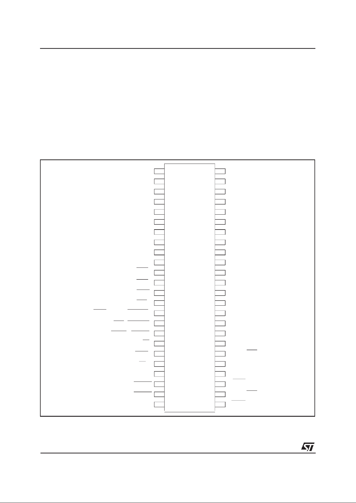
DIP48 PIN CONNECTION (Top view)
MK50H28
2/64
Page 3
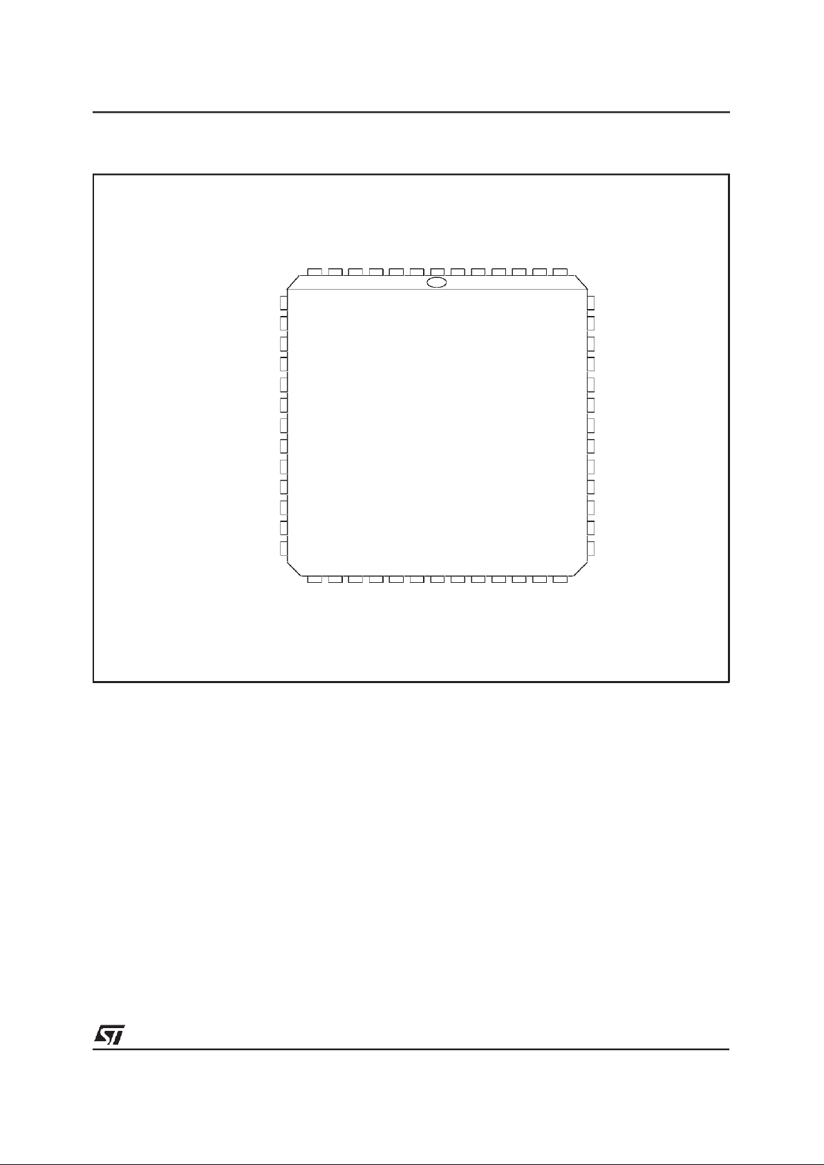
GND
DAL07
DAL06
DAL05
DAL04
DAL03
DAL02
DAL01
DAL00
READ
INTR
DALI
DALO
DAS
8
7 1 52 47
46
34
33
21
20
BMO/BYTE/BUSREL
No Connect
BM1/BUSAKO
HOLD/BUSRQ
ALE/AS
HLDA
CS
ADR
READY
RESET
GND
TCLK
No Connect
DTR/RTS
RCLK
SYSCLK
TD
DSR/CTS
RD
A23
No Connect
A22
A21
A20
A19
A18
A17
A16
DAL15
DAL13
DAL14
VCC
DAL08
DAL09
DAL10
DAL11
DAL12
No Connect
MK50H28Q
PLCC52 PIN CONNECTION(Top view)
MK50H28
3/64
Page 4
SIGNAL NAME PIN(S) TYPE DESCRIPTION
DAL<15:00> 2-9
40-47
[2-10
44-51]
IO/3S The time multiplexed Data/Addressbus. During theaddress portion of a
memory transfer, DAL<15:00> contains the lower16 bits of the memory
address.
During the data portion of a memory transfer, DAL<15:00> contains the read
or write data, depending on the typeof transfer.
READ 10
[11]
IO/3S READ indicatesthe type of operation that the bus controller is performing
during abus transaction. READ is driven by the MK50H28 only while it isthe
BUS MASTER. READ isvalid during the entire bus transaction and is
tristated at all other times.
MK50H28 as a BusSlave :
READ = HIGH - Data is placed on the DAL linesby the chip.
READ = LOW - Data is taken off the DAL lines bythe chip.
MK50H28 as a BusMaster :
READ = HIGH - Data is taken off theDAL lines by the chip.
READ = LOW - Data is placed on the DAL lines by the chip.
INTR 11
[12]
O/OD INTERRUPT is an attention interrupt line that indicates thatone or more of
the following CSR0 status flags is set: MISS, MERR, RINT, TINT or PINT.
INTERRUPT is enabled by CSR0<09>, INEA=1.
DALI 12
[13]
O/3S DALIN is an external bus transceiver control line. DALI is drivenby the
MK50H28 only while it is the BUS MASTER. DALIis asserted by the
MK50H28 when it readsfrom the DAL lines during the data portion of a
READ transfer. DALIis not asserted during a WRITE transfer.
DALO 13
[14]
O/3S DALOUT is an external bus transceiver control line. DALO is driven by the
MK50H28 only while it is the BUS MASTER. DALO is asserted by the
MK50H28 when it drivesthe DAL linesduring the address portionof a READ
transfer or for the durationof aWRITE transfer.
DAS 14
[15]
IO/3S DATA STROBE defines the data portion of a bus transaction. By definition,
data is stable and valid at the low tohigh transition of DAS. This signal is
driven by the MK50H28 while it is the BUS MASTER. Duringthe BUS
SLAVE operation, this pin is used as an input. At all other times the signal is
tristated.
BMO
BYTE
BUSREL
15
[16]
IO/3S I/O pins 15 and 16 are programmable through CSR4. If bit06 of CSR4 is set
to a one, pin 15 becomes input BUSREL and is usedby the host to signal
the MK50H28 to terminate a DMA burst after the current bus transfer has
completed. If bit 06 is clear then pin 15 is an outputand behavesas
described belowfor pin16.
BM1
BUSAKO
16
[18]
O/3S Pins15 and 16 are programmable through bit 00 of CSR4 (BCON).
If CSR4<00> BCON = 0,
I/O PIN 15 = BMO (O/3S)
I/O PIN 16 = BM1 (O/3S)
BYTE MASK<1:0> Indicates the byte(s) on the DAL to be read or written
during thisbus transaction. MK50H28 drives these lines only as a Bus
Master. MK50H28 ignores the BM lineswhen it is a Bus Slave.
Byte selectionis done as outlined in the following table.
BM1 BM0 TYPE OF TRANSFER
LOW LOW ENTIRE WORD
LOW HIGH UPPER BYTE
(DAL<15:08>)
HIGH LOW LOWER BYTE
(DAL<07:00>)
HIGH HIGH NONE
TAble 1 - PIN DESCRIPTION
LEGEND:
I Inputonly O Outputonly
IO Input/ Output 3S 3-State
OD OpenDrain (no internalpull-up)
Note: Pin out for 52 pin PLCCis shown in brackets.
MK50H28
4/64
Page 5
Table 1: PIN DESCRIPTION(continued)
SIGNAL NAME PIN(S) TYPE DESCRIPTION
If CSR4<00> BCON = 1,
I/O PIN 15 = BYTE (O/3S)
I/O PIN 16 = BUSAKO(O)
Byte selectionis done using the BYTE line and DAL<00> latched during the
address portion of thebus transaction. MK50H28 drives BYTE onlyas a Bus
Master and ignores it when a Bus Slave. Byte selection is done as outlined
in thefollowing table.
BYTE DAL<00> TYPE OF TRANSFER
LOW LOW ENTIRE WORD
LOW HIGH ILLEGAL CONDITION
HIGH LOW LOWER BYTE
HIGH HIGH UPPER BYTE
BUSAKOis a bus request daisy chainoutput. If MK50H28 is not requesting
the bus and it receives HLDA, BUSAKOwill be driven low. If MK50H28is
requesting the bus when it receives HLDA, BUSAKO will remain high
Note: All transfers are entireword unless the MK50H28 is configured for 8 bit
operation.
HOLD
BUSRQ
17
[19]
IO/OD Pin 17 is configured through bit 0 of CSR4.
If CSR4<00> BCON = 0,
I/O PIN 17 = HOLD
HOLD requestis assertedby MK50H28 when it requires a DMA cycle, if
HLDA is inactive, regardless of the previousstate of the HOLD pin. HOLD is
held low for the entireensuing bustransaction.
If CSR4<00> BCON = 1,
I/O PIN 17 = BUSRQ
BUSRQis asserted by MK50H28 when it requires a DMA cycle ifthe prior
state ofthe BUSRQ pin was high and HLDA is inactive. BUSRQ is held low
for the entire ensuing bus transaction.
ALE
AS
18
[20]
O/3S Theactive level of ADDRESS STROBE is programmablethrough CSR4.
The address portion of a bustransfer occurs while this signal isat its
asserted level.This signal is driven by MK50H28 whileit is theBUS
MASTER. At all other times, the signalis tristated.
If CSR4<01> ACON = 0,
I/O PIN 18 = ALE
ADDRESS LATCH ENABLE isused to demultiplex the DAL lines anddefine
the address portion of the transfer. As ALE, the signaltransitions from high
to low during the address portion of the transferand remains low during the
data portion.
If CSR4<01> ACON = 1,
I/O PIN 18 = AS
AsAS, the signal pulses low during the address portion of the bus transfer.
The low to hightransition of AS can beused by a slave deviceto strobe the
address into a register.
ASis effectively the inversion of ALE.
HLDA 19
[21]
I HOLD ACKNOWLEDGE is theresponse to HOLD. When HLDA is low in
response to MK50H28’s assertion of HOLD, the MK50H28 is theBus
Master. HLDA should bedeasserted ONLY after HOLD has been released
by the MK50H28.
CS 20
[22]
I CHIP SELECT indicates, when low, that theMK50H28 is the slave device
for the data transfer. CS must bevalid throughout the entire transaction.
ADR 21
[23]
I ADDRESS selects the Register Address Port or the Register Data Port. It
must be valid throughout thedata portion of the transfer and is only used by
the chip when CS is low.
ADR PORT
LOW REGISTER DATA PORT
HIGH REGISTER ADDRESS PORT
READY 22
[24]
IO/OD When the MK50H28 is a Bus Master, READY is an asynchronous
acknowledgement from the busmemory that memory willaccept data in a
WRITE cycle or thatmemory hasput data on the DAL lines in a READ cycle.
MK50H28
5/64
Page 6
Table 1: PIN DESCRIPTION(continued)
SIGNAL NAME PIN(S) TYPE DESCRIPTION
As a Bus Slave, theMK50H28 asserts READY when ithas put dataon the
DAL lines during a READ cycle or is about to take data from the DAL lines
during aWRITE cycle.READY is a response to DASand it willbe released
after DAS or CS is negated.
RESET 23
[25]
I RESET is the Bus signal that willcause MK50H28 to cease operation, clear
its internal logicand enter an idle state with the Power Offbit of CSR0 set.
TCLK 25
[28]
I TRANSMIT CLOCK. A 1x clock input for transmitter timing. TD changes on
the falling edge ofTCLK. Thefrequency of TCLK may not be greaterthan
the frequency of SYSCL
DTR
RTS
26
[29]
IO DATA TERMINAL READY, REQUEST TO SEND. Modem control pin. Pin
26 isconfigurable through CSR5. This pin can be programmed tobehave as
output RTS or as programmable IO pin DTR. If configured as RTS, the
MK50H28 will assert this pin if it has datato send andthroughout the
transmission ofa signal unit.
RCLK 27
[30]
I RECEIVE CLOCK. A 1x clock input for receiver timing. RD is sampled on
the rising edge of RCLK. The frequency of RCLK may not be greater than
the frequency of SYSCLK.
SYSCLK 28
[31]
I SYSTEM CLOCK. System clock used for internaltiming of theMK50H28.
SYSCLK should be as defined in the Electrical Specifications in Section 5.
TD 29
[32]
O TRANSMIT DATA. Transmit serial data output.
DSR
CTS
30
[33]
IO DATA SET READY, CLEAR TO SEND. Modem ControlPin. Pin 30 is
configurable through CSR5. This pin can be programmed tobehave as input
CTS oras programmable IO pin DSR. If configuredas CTS, the MK50H28
will transmit all ones while CTS is high.
RD 31
[34]
I RECEIVE DATA. Received serial data input.
A<23:16> 32-39
[37-43]
o/3s Address bits <23:16> used in conjunction withDAL<15:00> to produce a 24
bit address. MK50H28 drives these lines onlyas a Bus Master. A23-A20
may be driven continuously as described in the CSR4<7> BAE bit.
VSS-GND 1,24
[1,26]
Ground Pins
VCC 48
[52]
Power Supply Pin
+5.0 VDC + 5%
SECTION3
OPERATIONAL DESCRIPTION
The STMicroelectronics MK50H28 Multi-Logical
Link Communications Controller device is a VLSI
product intended for high performance data communication applications requiring Frame Relay
Service on Permanent Virtual Circuits. The
MK50H28 will perform all frame formatting, such
as: frame delimiting with flags, FCS (CRC) generation and detection, and zero bit insertion and
deletion for transparency. The MK50H28 also includes a buffer management mechanism that allows the user to transmit and/or receive multiple
frames for each active channel or DLCI. Contained in the buffer management is an on-chip
dual channel DMA: one channel for receive and
one channelfor transmit.
The MK50H28 can be used with any popular 16
or 8 bit microprocessor. A possible system configuration for the MK50H28 is shown in Figure 1.
This document assumes that the processorhas a
byte addressablememory organization.
The MK50H28 will move multiple blocks of receive and transmit data directly in and out of
memorythroughthe Host’sbus.
The MK50H28 may be operated in full or half duplex mode. In half duplex mode the RTS and
CTS modem control pins are provided. In full duplex mode, these pins become user programmable I/O pins.
All signal pins on the MK50H28 are TTL compatible. This has the advantage of making the
MK50H28 independent of the physical interface.
As shown in Fig. 1, line drivers and receivers are
used for electrical connection to the physical
layer.
MK50H28
6/64
Page 7
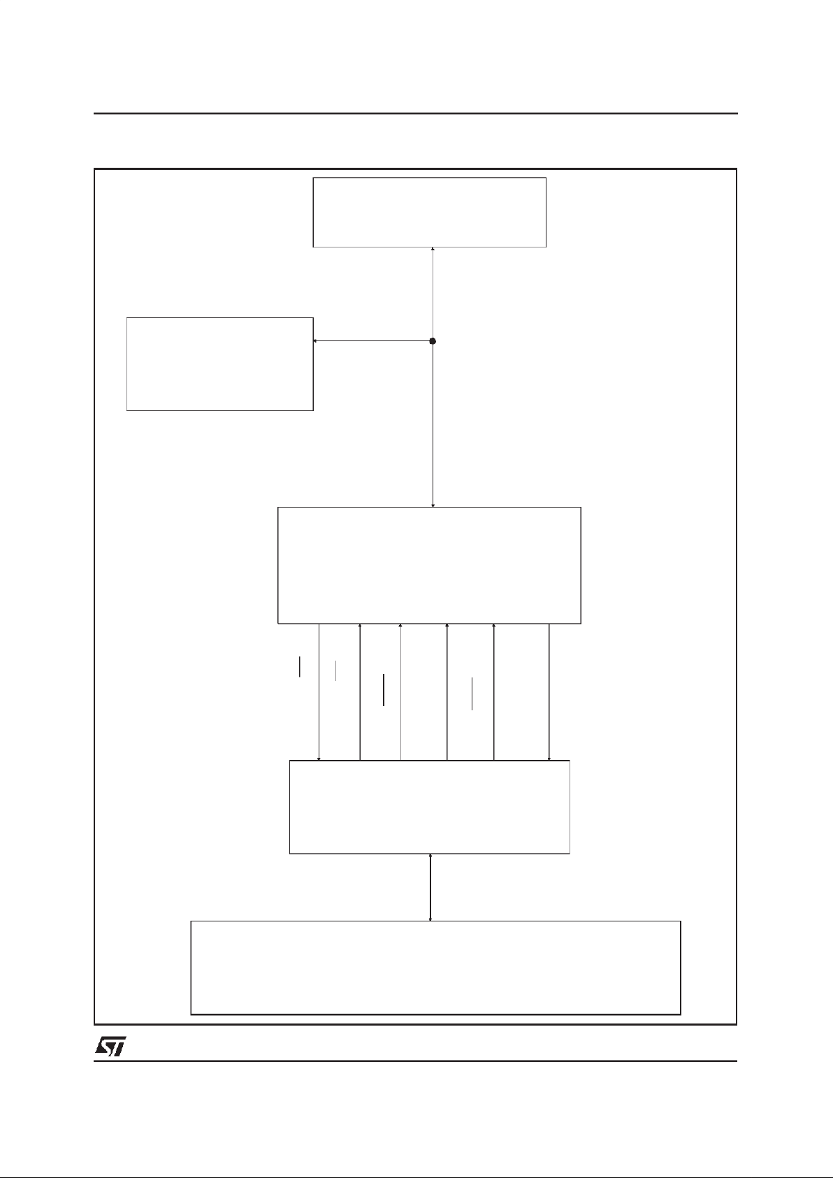
HOST PROCESSOR
(68000, 80186, Z8000, ETC)
16-BIT DATA BUS INCLUDING
24-BIT ADDRESS AND BUS CONTROL
MEMORY
(MULTIPLE
DATA BLOCKS)
MK50H28
RD
TD
LINE DRIVERS
AND RECEIVERS
(SUCH AS RS-449, RS-232C, V.35)
DATA COMM. CONNECTOR
ELECTRICAL I/O
(SUCH AS RS-232C, RS-423, RS-422)
TCLK
RCLK
DSR, CTS
DTR, RTS
Figure 1: PossibleSystemConfigurationfor theMK50H28
MK50H28
7/64
Page 8
DALI
DALO
HLDA
HOLD
ALE, AS
BM0
BM1
DAS
READ
INTR
ADR
READY
DTR, RTS
DSR, CTS
CS
FIRMWARE
ROM
MICRO
CONTROLLER
TIMERS
DMA
CONTROLLER
CONTROL / STATUS
REGISTERS 0 -5
SYSCLK
INTERNAL BUS
RECEIVER
FIFO
TRANSMITTER
FIFO
RECEIVER TRANSMITTER
LOOPBACK
TEST
RD
RCLK
TCLK
TD
VSS -GND
RESET
VCC
DAL <15:00>
A <23:16>
Figure 2: MK50H28SimplifiedBlock Diagram
MK50H28
8/64
Page 9

3.1 FunctionalBlocks
Refer tothe blockdiagram in Figure2.
The MK50H28 is primarily initialized and control-
led through six 16-bit Control and Status Registers (CSR0 thru CSR5). The CSR’s are accessed
through two bus addressable ports, the Register
Address Port (RAP), and the Register Data Port
(RDP). The MK50H28 may also generate an interrupt(s) to the Host. These interrupts are enabled and disabled through CSR0.
The on-chip microcontroller is used to control the
movement of parallel receive and transmit data,
and to handle the Addressfield filtering.
3.1.1 Microcontroller
The microcontrollercontrolsall of the otherblocks
of the MK50H28. The microcontroller performs
frame processing and protocol processing. All
primitive processing and generation is also done
here. The microcode ROM contains the control
program of the microcontroller.
3.1.2 Receiver
Serial receive data comes into the Receiver (Figure 2). TheReceiveris responsiblefor:
1. Leadingand trailing flag detection.
2. Deletionof zeroes inserted for transparency.
3. Detectionof idleand abortsequences.
4. Detectionof goodand bad FCS (CRC).
5. MonitoringReceiver FIFO status.
6. Detectionof ReceiverOver-Run.
7. Oddbytedetection.
NOTE: If frames are received that have an odd
number ofbytes thenthe lastbyte of theframe is
said tobe an odd byte.
8. Detectionof non-octetaligned frames.
Such frames are treatedas invalidframes.
3.1.3 Transmitter
The Transmitteris responsiblefor:
1. Serializationof outgoingdata.
2. Generatingand appending the FCS(CRC).
3. Framingthe outgoing frame with flags.
4. Zerobit insertionfor transparency.
5. TransmitterUnder-Run detection.
6. Transmissionof odd byte.
7. RTS/CTScontrol.
3.1.4 Frame Check Sequence or Cyclic RedundancyCheck
The FCS (CRC) on the transmitter or receiver
may be either 16 bit or 32 bit, and is user selectable. For full duplex operation, both the receiver
and transmitter have individual FCS computation
circuits. The characteristicsof the FCSare:
TransmittedPolarity: Inverted
TransmittedOrder: High Order Bit First
Pre-setValue: All 1’s
Polynomial16 bit:
X
16+X12+X5
+1
Remainder16 bit(if receivedcorrectly):
High orderbit-->0001 1101 0000 1111
Polynomial32 bit:
X
32+X26+X23+X22+X16+X12+X11+X10
+
+X
8+X7+X5+X4+X2
+X+1
Remainder32 bit(if receivedcorrectly):
high order bit-->11000111 00000100
11011101 0111 1011
3.1.5 Receive FIFO
The Receive FIFO buffers the data received by
the receiver. This performs two major functions.
First, it resynchronizes the data from the receive
clock to the system clock. Second, it allows the
microcontroller time to finish whatever it may be
doingbefore it has to process the receiveddata.
The receive FIFO holds the data from the receiver
without interrupting the microcontrolleruntil it contains enough data to reach the watermark level.
This watermark level can be programmed in
CSR4 to occur when the FIFO contains at least
18 or more bytes; 34 or more bytes; or 50 or
more bytes. Thisprogrammability, alongwith the
programmableburst length of the DMA controller,
enables the user to define how oftenand for how
long the MK50H28 must use the host bus. For
more information, see Control/StatusRegister 4.
For example, if the watermark level is set at 34
bytes and the burst length is limited to 8 word
transfers at a time, the MK50H28 will request
control of the host bus as soon as 34 bytes are
received and again after every 16 subsequent
bytes.
3.1.6 TransmitFIFO
The Transmit FIFO buffers the data to be transmitted by the MK50H28. This also performs two
major functions. First, it resynchronizesthe data
from the system clock to the transmit clock. Second, it allows the microcontroller and DMA controller to burst read data from the host’s memory
buffers; making both the MK50H28 and the host
bus more efficient.
MK50H28
9/64
Page 10

3.1.7 DMA Controller
The MK50H28has an on-chip DMA Controllercircuit. This allows it to access memory without requiring host software intervention. Whenever the
MK50H28 requires access to the host memory it
will negotiate for mastership of the bus. Upon
gaining controlof the bus theMK50H28 willbegin
transferring data to or from memory. The
MK50H28 will perform memory transfers until
either it has nothing more to transfer, it has
reached its DMA burst limit (user programmable),
or the BUSREL pin is driven low. In any case, it
will complete the current bus transfer before releasing bus mastership back to thehost. If during
a memory transfer, the memory does not respond
within 256 SCLK cycles, the MK50H28 will release ownership of the bus immediately and the
MERR bit will be set in CSR0. The DMA burst
limit can be programmed by the user through
CSR4. In 16 bit mode the limit can be set to 1
word, 8 words, or unlimited word transfers. In 8
bit mode,it can be set to 2 bytes, 16 bytes, or unlimited byte transfers. For high speed data lines
(i.e. > 1 Mbps) a burst limit of 8 words, 16 bytes
or unlimited is suggested to allow maximum
throughput.
The byte ordering of the DMA transfers can be
programmed to accountfor differences in processor architecturesor host programminglanguages.
Byte ordering can be programmed separately for
data and control information. Data information is
defined as all contents of data buffers; control information is defined as anything else in the
shared memory space (i.e. initializationblock, descriptors, etc). For more information see section
4.1.2.5 onControl and StatusRegister 4.
3.1.8 Bus Slave Circuitry
The MK50H28 contains a bank of internal control/status registers (CSR0-5) which can be accessed by the host as a peripheral. The host can
read or write to these registers like any other bus
slave. The contents of theseregistersare listedin
Section 4 and bus signal timing is described in
Figures 13 and 14.
3.2 Memory/Buffer ManagementOverview
The MK50H28 memory structure (Fig. 3) consists
of various blocks of off-chip memory. Only the
Control/Statusregisters,some RAM and firmware
ROM are onboard the chip. The Initialization
Block, Priority DLCI Block, Status Buffer, Address
Lookup Table (ALT), Context Table (CT), Transmit/Receive Rings and Buffers are in the off-chip
memory.
The buffer management is a circular queue of
tasks in memory called descriptor rings. There
are separate rings to describe the transmit and
receive operations. The MK50H28 buffer management mechanism will handle data frames
which are longer than the length of an individual
buffer. This is done by a chaining method which
utilizes multiple buffers. The MK50H28 tests the
next segment in the descriptor ring in a lookahead manner. If the packet is too long for one
buffer, the next buffer will be used after filling the
first buffer (that is chained to the previous buffer).
The MK50H28 will then look ahead to the next
buffer, and chain that buffer also if necessary,
and so on.
3.2.1 InitializationBlock
The MK50H28 initialization information is located
in a block of off- chip memory called the Initialization Block. The Initialization Block consists of 44
contiguous words of memory starting on a word
boundary. The starting address for the initialization block, IADR, is defined in the CSR2 and
CSR3 registers inside the MK50H28. This memory is assembled by the HOST, and the first 15
words are accessed by the MK50H28 during initialization. The Initialization Block (refer to section 4.2) is comprisedof:
A. Mode of Operation.
B. The nN1, nN2, andnN3 counters.
C. The dN1(MaxFrameLength) counter.
D. The nT1,nT2and TP (Transmit Polling)timers.
E. Pointer to thebeginningof Context Table.
F. PointertothebeginningofAddressLookupTable.
G. Pointer to the beginning of StatusBuffer.
H. Error Countersand Statistics.
3.2.1.1 Priority DLCI Block (PDB)
The Priority DLCI Block consists of ContextTable
indices for the priority channels. These indices
are a mechanism through whichthe host can demand the MK50H28 to immediately service certain desired DLCIs. The host should first set up
entries in the PDB before setting the PTDMD bit
in CSR2. In response to that, the MK50H28, after
completing transmission service of its current
DLCI, will jump to the PDB rather than advancing
to the next entry in the contexttable. Afterservicing all active entries in the PDB, the MK50H28
will return to the Context Table and resume the
transmission service that was in progress before
it was interrupted.
3.2.1.2 InterruptDescriptorRings
The MK50H28 has two descriptor ring structures
for the purpose of queing Transmit and Receive
interrupts. The pointers to these two descriptor
rings are located at IADR+24 thru IADR+30 in the
initialization Block. These descriptor rings are of
MK50H28
10/64
Page 11

a fixed size of 128 entries each. Each entry will
consist of two 16-bit words containing the24-bit
address of the context table entry (XCTADR or
RCTADR) corresponding to the interrupt, a 7-bit
field for the descriptor index (CURXD or CURRD)
into the associated descriptor ring, and a bit
SRVC which is used to indicate whether the interrupt has been serviced. The SRVC bit is set by
the MK50H28when it writes an interruptto the interrupt ring, and it should be cleared by the host
when it services the interrupt. If the MK50H28 attempts to write an interrupt to the interrupt descriptor ring and finds that SRVC is not clear then
it will issue a Provider Primitive 7 to indicate an
Interrupt Ring MISS (with PPARM=0 to indicate a
Receive Interrupt Ring MISS or PPARM=1to indicate a Transmit Interrupt Ring MISS).
3.2.2 AddressLookup Table(ALT)
The ALT contains the maximum of 1024 or 8192
addresses formed by the Data Link Connection
Identifier (DLCI). The MK50H28can support upto
4 octets of address field. The ALT is used to identify which of the 1024 or 8192 addresses are active. For each active channel it has an Index to
the Context Table(CT). The ALT is only used by
the receive processof the MK50H28.
3.2.3 Context Table(CT)
The MK50H28 performs multi-tasking by means
of a Context Table. Each entry in this table contains all the information relevant to one DLCI
channel. Associated with each DLCI are a set of
descriptor rings that are used for transmittingand
receiving frames. All channel entries, except the
LMI Channel,, have equal priority. The MK50H28
scans each entry in the CT sequentially, or
through the use of an index pointer mechanism,
for any available frames to be transmitted. When
a User Primitive 8 with UPARM=2 is issued to the
MK50H28. polling of the LMI/LIV channel will be
enabled to occur between each poll of the other
CT entries.
3.2.4 TransmitDescriptor Ring(s)
The transmit descriptor ring is a circular queue of
tasks that point to data buffers.A variable number
of buffers may be queued-upon a descriptorring
awaiting execution by the MK50H28. The descriptor ring has a segment assigned to each
buffer. Each segment holds a pointer for the
starting address of the buffer, and holds values
for the length of the buffer and the length of the
frame to be transmitted. Each segmentalso contains an OWNA control bit to denote whether the
MK50H28, or the HOST ”owns” the buffer. For
transmit,when the MK50H28 owns the buffer, the
MK50H28 is allowed and commandedto transmit
the contents of the buffer. When the MK50H28
does not own the buffer, it will not transmit the
data in that buffer.
3.2.5 Receive Descriptor Ring(s)
The receive descriptor ring is circular queue of
tasksthat point todata buffers.A variablenumber
of buffers may be queued-upon a descriptor ring
awaiting execution by the MK50H28. The descriptor ring has a segment assigned to each
buffer. Each segment holds a pointer for the
starting address of the buffer, and holds values
for the length of the buffer and the length of the
frame received. Each segment also contains an
OWNA control bit to denote whether the
MK50H28, or the HOST ”owns” the buffer. For
receive, when the MK50H28 owns the buffer, the
MK50H28 may place received data into that buffer. Conversely, when the MK50H28 does not
own a receive buffer, it will not place received
data in that buffer.
3.2.6 Frame Format
The frame format supported by the MK50H28 is
shown below. Each frame may consist of a programmable number of leading flag patterns
(01111110),an address field, an information field,
an FCS (CRC) of either 16 or 32 bits, and a trailing flag pattern. The number of leading flags
transmitted is programmable through the Mode
Registerin the InitializationBlock. The MK50H28
is capable of transmitting and receiving a single
flag between adjacentframes.
TRANSMITTED FIRST
3.2.7 MK50H28 Supported Frame Types
The MK50H28 supports all frame types shown in
Table 1. In LMI, both User and Network Modes
of operation, along with ”Optional Bidirectional
Network Procedures” (Annex D, ANSI T1.617 -
1991)are supported.
ADDRESS INFO FLAG
16/24/32
8*n
8
FLAG
FCS
8 16/32
MK50H28
11/64
Page 12
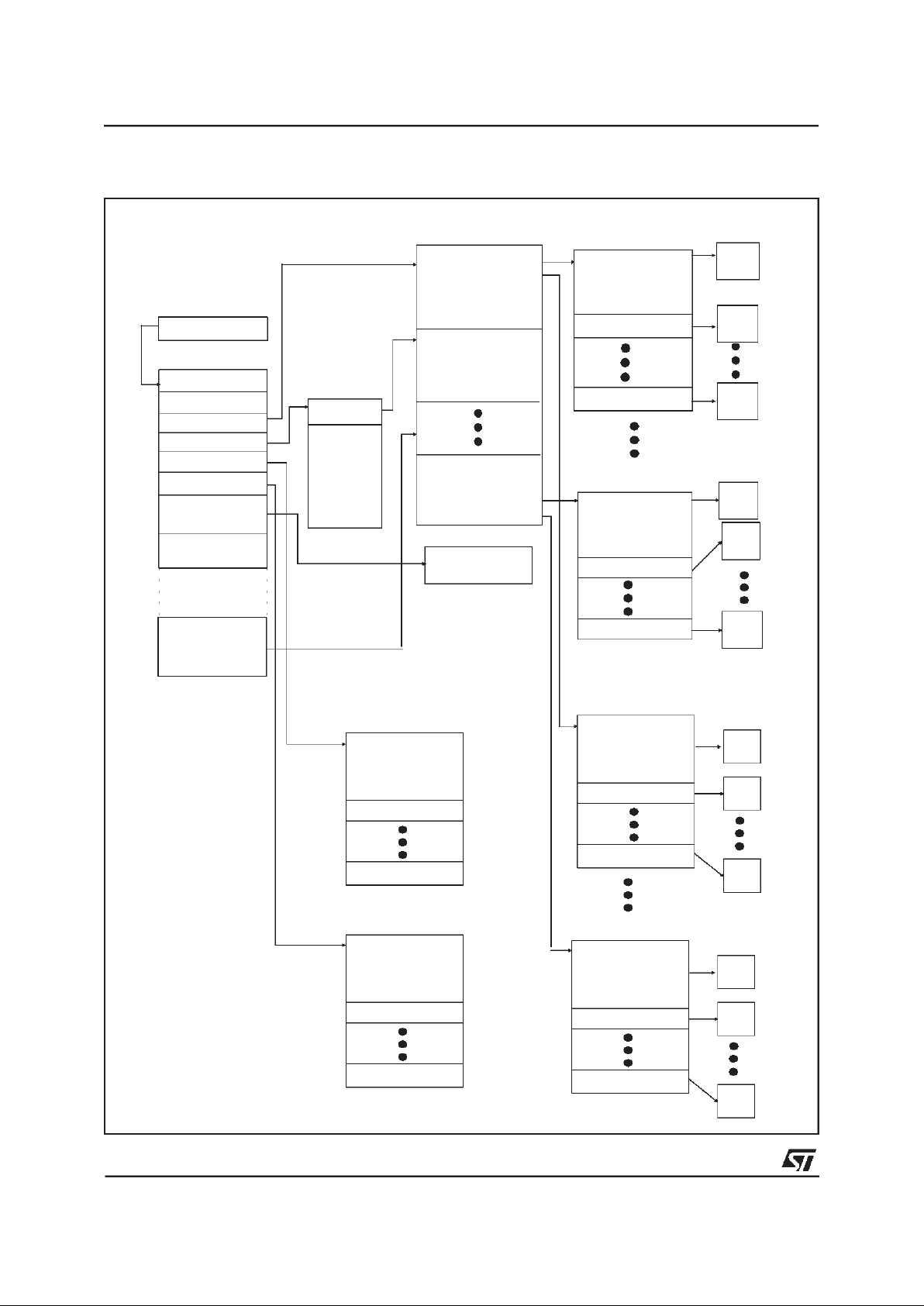
INIT BLOCK
PTR TO INIT
MODE
PTR TO ALT
PTR TO STATUS
PTR TO CT
ADDRESS
LOOKUP
TABLE
RING0XMIT
BUFF
0
BUFF ADDRESS
BUFF SIZE
BUFF MSG CNT
DESC 0
TIMER VALUES
ACT. CHNL
(1 ENTRY/ACT. CHNL)
BUFFERS
DATA
ACTIVE CHNL. 1
ACTIVE CHNL. N
TABLECONTEXT
RING NXMIT
BUFF SIZE
BUFF MSG CNT
DESC 0
DESC 1
DESC M
BUFF
M
DESC 1
DESC N
BUFF ADDRESS
BUFF
1
BUFF
1
BUFF
N
LMI ERROR
STATUS
BUFFER
CSR2, CSR3
COUNTERS
BUFF
0
RX RING N
DESC 0
DESC 1
BUFF
0
BUFF
Y
DESC Y
BUFFERS
DATA
BUFF ADDRESS
BUFF SIZE
BUFF MSG CNT
BUFF
1
RX RING 0
DESC 0
DESC 1
BUFF
0
BUFF
X
DESC X
BUFFERS
DATA
BUFF ADDRESS
BUFF SIZE
BUFF MSG CNT
BUFF
1
DESC RING PTRS
ACTIVE CHNL. 0
CONG STATISTICS
DLCI /ADDRESS
CONG STATISTICS
DLCI / ADDRESS
DESC RING PTRS
CONG STATISTICS
DLCI / ADDRESS
DESC RING PTRS
BUFFER
(DLCI 0
to
DLCI 1024
PRIORITY DLCI
BLOCK
or
DLCI 8192)
RX INTERRUPT RING
DESC 0
DESC 1
DESC 127
RX CT Address
Current RX Desc
Service Bit
TX INTERRUPT RING
DESC 0
DESC 1
DESC 127
TX CT Address
Current TX Desc
Service Bit
PTR TO TINT DR
PTR TO RINT DR
Figure 3: MK50H28Memory Management Structure
MK50H28
12/64
Page 13

3.2.8 Modes of ProtocolOperation
The User modeof operation is entered by issuing
an Auto LMI primitive 7 with UPARM=0. In this
mode, the device transmits STATUS ENQUIRY
messages to the network with an interval determined by the nT1timer. After every nN1 transmissions of STATUS ENQUIRY with Report Type of
”Length Integrity Verification (LIV) Only” the
MK50H28 transmits a STATUS ENQUIRY with
Report Type of ”FullStatus”.
When a STATUS frame is received in response to
a STATUS ENQUIRY(LIV only), the receive sequence number received from the Network side
is checked against the User send sequence number. A received Full STATUS frame will be stored
into the LMI/LIV channel buffer, the sequence
number checkingwill be performed,and its reception will be indicated to the host via Provider
Primitive 13. An availabletransmit or receive buffer is not required for the MK50H28 automatic
processingof ”LIVonly” frames.
A received Asynchronous STATUS frame will be
stored into the LMI/LIV channel buffer and its reception will be indicated to the host via Provider
Primitive 14. If a STATUS ENQUIRY frame (Full
or LIV only) is received in this mode of operation,
the MK50H28 will discard the frame and increment the Discarded Frames Counter in Context
Table enrtry 0. Also see nT1 description in 4.2.2
Timer/Countersection.
The Network mode of operation is enteredby is-
suing an Auto LMI primitive 7 with UPARM=1. In
this mode, the device automatically responds to
STATUS ENQUIRY with Report Type of ”Length
Integrity Verification (LIV) Only” by transmitting a
STATUS frame with Report Type of ”LIV Only”
along with restarting the nT2 timer. An available
transmit or receive buffer is not required for the
MK50H28 automatic processing of ”LIV only”
frames.
When a STATUS ENQUIRY with Report Type of
”Full Status” is received, the device issues the
LMI Received primitive 13 (with PPARM=1) and
expects the host to respond with an LMI Status
Request Primitive 11 with UPARM=0 (when the
host is readyto transmitthe Full STATUSframe).
Asynchronous STATUS frames may be transmitted by placing the data to be transmitted into the
appropriate buffer and issueing Primtive 11 with
UPARM=2. If a STATUS frame(Full,LIV Only,or
Asynchronous)is received in this mode of operation, the MK50H28 will discard the frame and increment the Discarded Frames Counter in Context Table enrtry 0. Also see nT2 description in
4.2.2Timer/Countersection.
The Bi-directional Network Procedures mode
is entered by issuing an Auto LMI primitive 7 with
UPARM=2. The MK50H28 supports this operation using separate User and Network sequence
numbers and N392 and N393 counters. In this
mode, the device transmits STATUS ENQUIRY
messages with a User set of sequence numbers
at an interval determined by the nT1/T391 timer.
The expected response is a STATUS frame with
corresponding sequence numbers. After every
nN1/N391 transmissions of STATUS ENQUIRY
with Report Type of ”LIV Only”, the MK50H28
transmits a STATUS ENQUIRY with Report Type
of ”Full Status”.
A received Full STATUS frame will be stored into
the LMI/LIV channel buffer, the sequence number
checking will be performed, and its reception will
be indicated to the host via Provider Primitive 13.
A received Asynchronous STATUS frame will be
stored into the LMI/LIV channel buffer and its reception will be indicated to the host via Provider
Primitive 14.
In this mode, the device also automatically responds to STATUS ENQUIRY (”LIV Only”) by
transmitting a STATUS (”LIV Only”) frame along
with restarting the nT2 timer.Whena ”Full Status”
Table 1 - MK50H28Frame Types
INFORMATION ELEMENT NAME DIRECTION
Message Type Encoding
MSB LSB
Message Type STATUS_ENQUIRY User -> Network 0 1 1 1 0 1 0 1
STATUS Network -> User 0 1 1 1 1 1 0 1
UPDATE_STATUS Network <-> User 0 1 1 1 1 0 1 1
NOTES:
1. STATUS_ENQUIRY Frame - This Frame has the format as shown inFigure 4.
2. STATUS Frame - This Frame has the format as shownin Figure 5. If Full STATUS information is to be sent, the
host must specify the PVC_STATUS Information Element(s) in thetransmit buffer(s).
3. Asynchronous STATUS Frame - This Frame has the format as shownin Figure 6.The host must specify the PVC_
STATUS Information Elementin the transmit buffer(s).
4. UPDATE_STATUS Frame - Not used in most current applications, MK50H28 supported for backwards compatibility.
MK50H28
13/64
Page 14

STATUS ENQUIRY is received, the device issues the LMI Received primitive 13 (with
PPARM=1) and expects the host to respondwith
LMI Status Request Primitive 11 with UPARM=0
(when the host is ready to transmit the Full
STATUSframe).
Asynchronous STATUS frames may be transmitted by placing the data to be transmitted into the
appropriate buffer and issueing Primtive 11 with
UPARM=2.
LMI frames received in any mode will not cause
Receive Interrupts (RINT) to be generated, nor
will the Receive Interrupt Ring be updated. Instead, the MK50H28 will issue primitives corresponding to those LMI Frame received which are
not automaticallyprocessedby the MK50H28(i.e.
non ”LIV only” frames). See the description of
primitives in section 4.1.2.2. In addition to the
primitives, bits09-11 of the Receive MessageDescriptor0 (RMD0)for theLMI channelwill indicate
the type of frame received. See section 4.3.1.2
for details.
In Non-Auto-LMI mode of operation, LMI frames
received on the LMI Channel (typically DLCI 0)
will be writteninto the receive buffer as Transparent or SVC frames.
Also refer to DetailedProgramming Procedures
(section 4.4) for more information on using the
devicein thepreviously mentioned modes of ProtocolOperation.
MK50H28
14/64
Page 15

11111100
11110001
01111110
01010001
1
00000000
01010011
2
CURRENT SEQ
LAST RCVD SEQ
MANAGEMENT DLCI
UN-NUMBERED INFO FRAME
PROTOCOL DISCRIMINATOR
CALL REFERENCE (null)
STATUS MESSAGE
REPORT_TYPE IE
(Full STATUSMessage)
Link Integrity Verification IE
87654321
FCS (msb)
FCS (lsb)
01111110
FRAME FCS
00000011
00001000
00000000
01111101
01010111
3
PVC DLCI (msb)
PVC DLCI (lsb)
PVC_STATUS IE
00
1
0
00
1000N0A0
Figure 5: SampleAnnexA STATUSFrame (Full)
11111100
11110001
01111110
00000011
00001000
00000000
01110101
01010001
1
00000001
01010011
2
CURRENT SEQ
LAST RCVD SEQ
FCS (msb)
FCS (lsb)
01111110
MANAGEMENT DLCI
UN-NUMBERED INFO FRAME
PROTOCOL DISCRIMINATOR
CALL REFERENCE(null)
STATUS_ENQUIRY MESSAGE
REPORT_TYPE IE
(Requesting a LIV Only
STATUS Message)
Link Integrity Verification IE
FRAME FCS
87654321
Figure 4: SampleAnnexA STATUS_ENQUIRYFrame
MK50H28
15/64
Page 16
11111100
11110001
01111110
00000001
1
00000010
MANAGEMENT DLCI
UN-NUMBERED INFO FRAME
PROTOCOL DISCRIMINATOR
CALL REFERENCE (null)
STATUS MESSAGE
REPORT_TYPEIE
(AsynchronousSTATUS Message)
87654321
00000011
00001000
00000000
01111101
FCS (msb)
FCS (lsb)
01111110
FRAME FCS
00000111
1000N0A0
3
PVC DLCI (msb)
PVC DLCI (lsb)
PVC_STATUSIE
10010101
LOCKING SHIFT(ANSI Annex D Only)
1
00
000
Figure 7: SampleAsynchronousSTATUS Frame (AnnexD)
11111100
11110001
01111110
00000001
1
00000000
00000011
2
CURRENT SEQ
LAST RCVD SEQ
MANAGEMENT DLCI
UN-NUMBERED INFO FRAME
PROTOCOL DISCRIMINATOR
CALL REFERENCE (null)
STATUS MESSAGE
REPORT_TYPEIE
(Full STATUS Message)
LengthIntegrity VerificationIE
87654321
00000011
00001000
00000000
01111101
FCS (msb)
FCS (lsb)
01111110
FRAME FCS
00000111
1000N0A0
3
PVC DLCI (msb)
PVC DLCI (lsb)
PVC_STATUSIE
10010101
LOCKING SHIFT(ANSI Annex D Only)
1
00
000
Figure 6: SampleAnnexD STATUSFrame (Full)
MK50H28
16/64
Page 17

SECTION4
PROGRAMMINGSPECIFICATION
This section defines the Control and Status Registers and the memory data structures required to
program the MK50H28.
4.1 Control and StatusRegisters
There are six Control and Status Registers
(CSR’s) resident within the MK50H28. The
CSR’s are accessed through two bus addressable ports, an address port (RAP), and a data
port (RDP), thus requiring only two locations in
the system memoryor I/Omap.
4.1.1 Accessing the Contro l and Status Regi sters
The CSR’s are read (or written) in a two step operation.The address of theCSR is writteninto the
address port (RAP) during a bus slave transaction. During a subsequentbus slave transaction,
the data being read from (or written into) the data
port (RDP) is read from (or written into) the CSR
selected in the RAP. Once written, the address in
RAP remains unchanged until rewritten or upon a
bus reset. A control I/O pin (ADR) is providedto
distinguishthe address port fromthe data port.
ADR Port
4.1.1.1 Register AddressPort (RAP)
00000000
B
M
8
000
CSR
<2:0>
15141
3
0
7
0
8
1
0
1
1
1
2
0
1
0
2
0
3
0
4
0
5
0
0
0
9
0
6
H
B
Y
E
T
BIT NAME DESCRIPTION
15:08 RESERVED Must be written as zeroes
07 BM8 When set, places chip into 8 bit mode. CSR’s, Init Block, and data transfers are all 8 bit
transfers; this provides compatibility with 8 bitmicroprocessors. When clear, all transfers
are 16 bit transfers. This bitmust be set to the same valueeach time it is written,
changing this bitduring normal operation will achieve unexpectedresults. BM8 is
READ/WRITE and cleared on Bus RESET.
06:04 RESERVED Must be written as zeroes
03:01 CS3<2:0> CSR address select bits. READ/WRITE. Selects the CSR to be accessed through the
RDP. RAP is cleared by Bus RESET.
CSR<2:0> CSR
0 CSR0
1 CSR1
2 CSR2
3 CSR3
4 CSR4
5 CSR5
00 HBYTE Determines which byte isaddressed for 8 bit mode. If set,the high byte of the register
referred to by CSR<2:0> is addressed, otherwisethe low byte is addressed. This bit is
only meaningfulin 8 bit mode and must be written as zero if BM8=0.HBYTE is
READ/WRITE and cleared on bus reset.
MK50H28
17/64
Page 18

CSR DATA
1
5
1
0
1
4
0
9
121
1
0
8
0
3
0
7
0
2
06050
4
010
0
1
3
4.1.1.2 Register Data Port (RDP)
BIT NAME DESCRIPTION
15:00 CSR DATA Writing data to theRDP loads data into the CSR selected by RAP. Reading thedata from
RDP reads the data from the CSR selected in RAP.
15141
3
0
7
0
8
1
0
1
1
1
2
0
1
0
2
0
3
0
4
0
5
0
0
0
9
0
6
0
R
I
N
T
T
I
N
T
P
I
N
T
T
U
R
M
I
S
S
M
E
R
R
R
O
R
I
N
T
R
R
X
O
N
T
X
O
N
I
N
E
A
S
T
O
P
D
T
X
D
R
X
P
T
D
M
D
4.1.2 Control and Status Register Definition
4.1.2.1 Controland Status Register 0 (CSR0)
RAP<3:1> = 0
BIT NAME DESCRIPTION
15 PTDMD Transmit Demand for PriorityDLCIs. Setting this bit to1 causes the MK50H28 tojump to
Priority DLCI Block (PDB).This bit is cleared by the MK50H28 after servicing allactive
entries in the PDB. (Note: See section4.2.9 for moredetails.)
14 STOP STOP, when set,indicates that MK50H28 is operating in the STOPPED Phase of
operation. All external activity is disabled and internal logic is reset. MK50H28 remains
inactive except for primitive processinguntil a START primitive is issued. STOP IS READ
ONLY andset by BusRESET or a STOP primitive. Writing to this bit has no effect.
13 DTX Disable Transmitter. Prevents the MK50H28 from further access to the Transmitter
Descriptor Rings. No transmissionsare attempted after finishingtransmission of any
frame intransmission at the time of DTX beingset. Even LMI frames normallygenerated
automatically will not be transmitted if DTX=1. TXON acknowledges changes to DTX,
see below. DTX is READ/WRITE.
12 DRX Disable the Receiver prevents the MK50H28 from further access to the Receiver
Descriptor Rings. No received frames areaccepted afterfinishing reception of any frame
in receptionat the time of DRX being set. Setting DRX will put theMK50H28 in the
LOCAL BUSY Phase. RXON acknowledges changesto DRX, see description of RXON.
DRX is READ/WRITE.
MK50H28
18/64
Page 19

BIT NAME DESCRIPTION
11 TXON TRANSMITTER ON indicates that the transmit ring access is enabled.TXON is set as
the Startprimitive is issued if the DTX bit is”0” orafterward as DTX is cleared. TXON is
cleared upon recognition of DTX being set, by sending a Stop primitive in CSR1, or by a
Bus RESET. If TXON is clear, the host may modify the Transmit Descriptor Rings entries
regardless of the state of the OWNA bits. TXON is READ ONLY; writing to this bit has no
effect.
10 RXON RECEIVER ON indicates that the receive ring access is enabled. RXON is setas the
Start primitive is issued ifthe DRXbit is”0” or afterwardas DRX is cleared. RXON is
cleared upon recognition of DRX being set, by sending a Stopprimitive in CSR1, or by a
Bus RESET. RXON is READ ONLY; writing to this bit has no effect.
09 INEA INTERRUPT ENABLE allows the INTR I/O pin to be driven low when the Interrupt Flag
is set.If INEA = 1 and INTR = 1 the INTR I/O pin will be low.If INEA = 0 the INTR I/O
pin will be high, regardless of the state of the Interrupt Flag (TINT, RINT, or PINT) or
whether the Interrupt Desciptor Ring has been updated. INEA is READ/WRITE set by
writing a ”1” into thisbit and is cleared by writing a ”0” into this bit, byBus RESET, or by
issuing a Stop primitive. INEA may not be set while in the STOPPED Phase.
08 INTR INTERRUPT FLAG indicatesthat one ormore ofthe followinginterrupt causing
conditions has occurred: MISS, MERR, RINT, TINT, PINT. If INEA = 1 and INTR = 1 the
INTR I/Opin willbe low. INTR is READ ONLY, writing this bit has no effect. INTR is
cleared as the specificinterrupting condition bits are cleared. INTR is alsocleared by
Bus RESETor by issuing a Stopprimitive.
07 MERR MEMORY ERROR is set whenthe MK50H28is the Bus Master and READYhas not
been asserted within 256 SYSCLKs (25.6 usec @ 10MHz) after asserting the address on
the DALlines. When a Memory Error is detected, the MK50H28 releases the bus,
the receiverand transmitter areturned off, and an interrupt is generated if INEA = 1.
MERR is READ/CLEAR ONLY and isset by the chipand cleared by writing a ”1” intothe
bit. Writinga ”0”has no effect. It is cleared by Bus RESET or by issuing a Stop primitive.
06 MISS MISSED frame is set when the receiving channel loses a frame because it is either not
ready or does not own a receive buffer indicating loss of data. The Memory Address for
which MISS occurred can be determined by issuing a Status Request primitive (see
section 4.3.3 Status Buffer for additional details). When MISS is set, an interrupt will be
generated if INEA = 1. MISS is READ/CLEAR ONLY and is set by MK50H28 and
cleared by writing a ”1” into the bit. Writing a ”0” has no effect. It is also cleared by Bus
RESET or by issuing a Stop primitive.
05 ROR RECEIVER OVERRUN indicates that the Receiver FIFO was full when thereceiver was
ready to input data to the ReceiverFIFO. The frame being received is lost, butis
probably recoverable if an upper level protocol is used. When ROR is set, an interrupt is
generated if INEA=1. ROR is READ/CLEAR ONLY and is set by MK50H28 and
cleared by writing a ”1” into the bit. Writing a ”0” has no effect. It is also cleared by Bus
RESET or by issuing a Stop primitive.
04 TUR TRANSMITTER UNDERRUN indicates that the MK50H28 has aborted a frame since
data was late from memory. This condition is reached when the transmitter and
transmitter FIFO both become empty while transmitting a frame. WhenTUR isset, an
interrupt is generated if INEA = 1. TUR is READ/CLEAR ONLY and isset by MK50H28
and clearedby writing a ”1” into the bit. Writinga ”0” has no effect. It is also cleared by
Bus RESETor by issuing a Stopprimitive.
03 PINT PRIMITIVE INTERRUPT is set after the chip updates the primitive register to issue a
provider primitive. When PINT isset, an interruptis generatedif INEA =1. PINT is
READ/CLEAR ONLY and isset by MK50H28 and cleared by writing a ”1” into the bit.
Writing a ”0” has no effect. It is also clearedby Bus RESETor by issuing a Stop primitive.
02 TINT TRANSMITTER INTERRUPT is set after the chip updates an entry in theTransmit
Descriptor Ring.When TINT is set,an interrupt is generated if INEA = 1. TINT is
READ/CLEAR ONLY and isset by the MK50H28 and cleared by writing a ”1” into the bit.
Writing a ”0” has no effect. It is also clearedby Bus RESETor by issuing a Stop primitive.
01 RINT RECEIVER INTERRUPT is set after the MK50H28 updates an entry in the Receive
Descriptor Ring (this is done once per received frame, not per receivedbuffer). When
RINT is set, aninterrupt is generated if INEA = 1. RINT is READ/CLEAR ONLY and is
set by theMK50H28 and clearedby writing a ”1” into the bit. Writing a ”0” hasno effect.
It iscleared by Bus RESET or by issuing a Stop primitive.
00 0 This bit is READ ONLY and will always read as zero.
MK50H28
19/64
Page 20

1
5
1
0
1
4
0
9
121
1
0
8
0
3
0
7
0
2
06050
4
010
0
1
3
UPRIM
< 3:0 >
PPRIM
< 3:0 >
U
E
R
R
U
A
V
P
A
V
P
L
O
S
T
U
P
A
R
M
:
P
P
A
R
M
1
0
:
1
0
4.1.2.2 Controland Status Register 1 (CSR1)
RAP <3:1> = 133/
BIT NAME DESCRIPTION
15 UERR USER PRIMITIVE ERROR isset by the MK50H28 when a primitive is issued by the
user which is in conflictwith thecurrent status of the chip. UERR is READ/CLEAR
ONLY andis set by MK50H28 and cleared by writing a ”1” into the bit. Writing a ”0” in
this bit has no effect. It is also cleared by Bus RESET.
14 UAV USER PRIMITIVE AVAILABLE is set by the user when a primitive is written into UPRIM.
It iscleared by the MK50H28 after the primitive has been processed. This bit is also
cleared by a BusRESET.
13:12 UPARM USER PARAMETER is written by the host inconjunction with the user primitives in
UPRIM. This User Parameter fieldprovides information to the MK50H28 concerning the
corresponding user primitive. NOTE: For all primitives UPARM = 0 unless otherwise
indicated.
11:08 UPRIM USER PRIMITIVE is written by the user,in conjunction with setting UAV, to control the
MK50H28 linkprocedures. The following primitives are available:
0 Stop: Causes MK50H28 to enter the STOPPED Phase. All link activity is terminated
and theSTOP bit is set. All DMA activity ceases. The transmitter outputs all ones, and all
received data is ignored.
1 Start: Instructs the MK50H28 to exit theSTOPPED Phase and enter the INFORMATION
TRANSFER Phase. The Context Table and the Descriptor Rings are Reset. The
transmitter begins to output flags. The Start primitive isvalid only after the deviceis
initialized (Init Request performed.) If the Auto LMI primitive isnot issued after a Start
primitive, then the only way to transmit LMI frames is through the use of LMI
primitives (10, 11, 12, & 14), and processing is performed on received LMI frames,
but no automatic response or action is taken. Valid onlyin STOPPED phase.
2 Init Request: Instructs the MK50H28 toread the InitializationBlock frommemory. This
should be performed prior to the Start primitive or Transparent primitive after a bus reset
or power-up. Valid only in STOPPED phase.
3 Transparent Mode: Instructs the device to exit the STOPPEDPhase, enter the
TRANSPARENT Phase, and resetthe Context Table and Descriptor Rings. No header
stripping or pre-pending is done for any DLCI channel,and noautomatic LMI processing
is possibleinthis mode. All frames are received to Context Table entry 0 associated
descriptor ring and buffers, and the RTAN bit in CT0 should be set so that the entire
received frame will be written to the buffer. Transmission of frames can occur from
any ContextTable entry, including CT0, and theXTRAN bit should be set so that
only the data in the buffer willbe transmitted for the entire frame. This primitiveis only
valid after device Initialization (Init Request performed). Valid only in STOPPED phase.
4 Status Request: Instructs the MK50H28 to write the current chip status intothe
STATUS BUFFER. Valid in all states, but only after the Initprimitive has been previously
issued.
5 Self-Test Request: Instructs the MK50H28 to perform the built in internalself test. Valid
only in the STOPPED Phase. See section 4.4.10 for the self test procedure.
MK50H28
20/64
Page 21

BIT NAME DESCRIPTION
7 Auto LMI: Instructs the device to enter the Auto LMI Mode of operation.
Auto LMI with UPARM=0 causes the deviceto enter User mode of operation.
Auto LMI with UPARM=1 causes the deviceto enter Network mode of operation.
Auto LMI with UPARM=2 causes the deviceto enter Bi-directional mode of operation
These modes are defined in sections 3.2.7 and 3.2.8(Modes of Protocol Operation)
Valid only in INFORMATION TRANSFER phase. See also Start primitive.
8 Start Timer nT1(UPARM=0): Instructs the MK50H28 to start the nT1 (User) timer.
Issuing this primitive while in the User mode of Auto LMI operationmay leadto erroneous
results. Not valid in TRANSPARENT Mode.
Enable LMI Channel Polling (UPARM=2): Instructs the MK50H28 to start polling the
LMI Channel(Context TableEntry 0) for any LMI frames to be transmitted. The type of
LMI frame to be transmitted will be determined by the Frame Type bits in the TMD0 (see
section 4.3.2.2). The polling of the LMI Channel will beinterleaved between polling each
other CT Entry or channel, thus giving the LMI Channel a high degree of priority.
Disable LMI Channel Polling (UPARM=3): Instructs the MK50H28 to stop pollingof the
LMI Channel. The defaultinitialization condition of the MK50H28 is for LMI Channel
Polling to be disabled, so this primitive only need be issued if polling was enabled earlier.
9 Start Timer nT2: Instructs the MK50H28 to start thenT2 (Network) timer. Issuing this
primitive while in the Network mode of Auto LMI operation may lead to erroneous results.
Not validin TRANSPARENT Mode.
10 LMI STATUS_ENQUIRY Request: Instructs the MK50H28 to senda
STATUS_ENQUIRY frame to theremote site (network). If UPARM = 1,will request
Sequence Numbers only. Otherwise, requests Full STATUSframe. Not valid in
TRANSPARENT Mode.
11 LMI STATUS Request: Instructs the MK50H28 to send a STATUS frameto the remote
site (user).
If UPARM=0, it willsend a FULL STATUS framewith the data inthe associated LMI
Channel buffer (this is a typical response to a received STATUS ENQUIRY with Report‘
Type of FULL STATUS).
If UPARM = 1, it willsend a SequenceNumbers Only (LIV Only) frame.
If UPARM=2, it willsend an Aysnchronous STATUS frame with the data inthe associated
LMI Channelbuffer. Notvalid in TRANSPARENT Mode.
12 LMI UPDATE_STATUS Request: Instructs MK50H28 tosend UPDATE_STATUS frame
with thedata in the associated LMI Channel buffer. Not valid in TRANSPARENT Mode.
13 Receive LMI Full Status Enquiry Request (UPRIM =13,UPARM=0); Instructs the
MK50H28 to cause the next receivedSequence Number Only (LIV Only) Status Enquiry
Frame to be received to a buffer, as if it were a FULL STATUS ENQUIRY Frame.
However, thestatistics corresponding to the actual type offrame received wil be
incremented No response frame will be automatically generated by the MK50H28.
Issueing UPRIM 13 with UPARM =1 prior to receipt of the next LIVOnly Status Enquiry
Frame willcancel the action originally requested by the Receive LMIFull Status Enquiry
Request Primitive.
14 Send LMI: Instructsthe chip to senda frame using the contents ofthe buffer(s) pointed to
by the Context Table LMI Channel (either 0 or 1023 based upon the setting of
LMICH bit in CSR2). The frame will be transmitted using the header information from
the ContextTable LMI Channel. Valid in all Phases of operation except for STOPPED
mode. NOTE: Only one frame will be transmitted per Send LMI primitive.
15 Indicate Protocol Event: Thisprimitive can be used by thehost to informthe MK50H28
of errored eventsnot monitoredby the chip (suchas areceived PVC status IE withNew
bit=0 for a PVC not currently defined)
If UPARM=0, it instructsthe MK50H28 to add one good event to the N392/nN2 count.
If UPARM=1, it instructsthe MK50H28 to add one errored eventto the N392/nN2 count.
MK50H28
21/64
Page 22

BIT NAME DESCRIPTION
07 PLOST PROVIDER PRIMITIVE LOST is set by the MK50H28 when a provider primitive cannot
be issuedbecause thePAV bit is still set fromthe previousprovider primitive. PLOST is
cleared when PAV is cleared or by a Bus RESET. Writing to this bit has no effect.
06 PAV PROVIDER PRIMITIVE AVAILABLE is set by the MK50H28 when a new provider
primitive has been placed in PPRIM. PAV is READ/CLEAR ONLY and isset by the chip
and clearedby writing a ”1” to the bit or by Bus RESET. Under normal operation the host
should clear the PAV bit after PPRIM is read.
05:04 PPARM PROVIDER PARAMETER provides additional information about the reason for the
receipt of certain primitives. The following table shows the parameters for the applicable
provider primitives. This field is undefined for other provider primitives.
03:00 PPRIM PROVIDER PRIMITIVE is written by the MK50H228, in conjunction with setting the PAV
bit, to inform theuser of link control conditions. ValidProvider Primitives are as follows:
2 Init Confirmation: Indicates MK50H28 Init Block reading has completed.
3 Watchdog Timer Expiry Indication: Indicates expirationof TCLK or RCLK watchdog
timer as determined by the value of PPARM (PPARM=1 indicatesTCLK, PPARM=2
indicates RCLK. If PLOSTis set it indicates both RCLK and TCLK watchdog timers
expired). This primitive is issued only ifenabled by setting CSR5<15:12> bits to
something other than 0.
4 Alarm Indication: nN2 of thelast nN3 LMI events are corrupted intiming or content.
6 Alarm Clear Indication: Indicates reception of nN3 correct sequential LMI events after
the AlarmIndication. The issueingof Alarm Clear Indication and Alarm Indication
primitives willbe re-attempted if PLOST is set, and willbe repeated until issued without
PLOST set.
7 Interrupt Descriptor Ring MISS: Indicates inability to write to the InterruptDescriptor
Ring dueto the SRVC bit not being clear.With PPARM = 0it indicates aTransmit
Interrupt Ring MISS. With PPARM = 1 it indicates a Receive Interrupt Ring MISS.
8 Timer nT1 Expiration: Indicates expiration of the timer nT1.
9 Timer nT2 Expiration: Indicates expiration of the timer nT2.
10 Counter nN1 Overflow: Indicates that the counter nN1 has overflowed.
11 Clear New Bit Indicatiojn: This primitive is issued when the sequencenumber received
in aStatus Enquiry frame matches the sequence number sent in the last Full Status
frame.
12 LMI Frame Transmitted: Indicates that a LMI frame was just transmitted.
13 LMI Frame Received: Indicates that a LMI framewas just received and stored in the
buffer(s) corresponding to the LMI channel. The PPARM fieldwill indicate the type of
frame received.In Auto LMI mode, a required host response to areceived STATUS
ENQUIRY with Report Type of FULL STATUS is to issue an LMI STATUS Request
primitive with UPARM = 0 (STATUS Request with Report Type of FULL STATUS). The
device will not automatically respond to areceived STATUS ENQUIRY with Report Type
of FULL STATUS.
Note: If a LMI frame is received whilethe PAV bit is still set (because a previously
received primitive has not yet been processed by the host), the MK50H28 will set the
PLOST bitand the received LMI frame will be discarded. No counters will be updated.
14 Aysnchronous STATUS Frame Received: Indicates that an Aysnchronous STATUS
frame was justreceived. Received AysnchronousSTATUS frames are stored in the LMI
channel buffer without the DLCI header information.
PPARM LMI Frame Received
0 STATUS ENQUIRY withReport Type of Sequence
Numbers Exchange Only
1 STATUS ENQUIRY with Report Type ofFULL STATUS
2 STATUS frame received
3 SVC or UPDATED STATUS frame received
MK50H28
22/64
Page 23

BIT NAME DESCRIPTION
15 CYCLE Setting this bitselects a shorterDMA Cycle (5 vs 6 SYSCLK)
14 EIBEN Extended Initialization BlockEnable. Setting thisbit causes the MK50H28 to use an
extended Initialization Block which uses all of IADR+08 as a 16-bit scaler and moves nN1
to the upper byte ofIADR+40.
13 DLCI1K Setting this bit causes the chipto recognize the 8192 possibleDLCIs.If this bit is cleared,
the chipwill ignore all received frames with DLCIgreater than 1023.
12 LMICH CHLMI Channel Select: Settingthis bit to 0 causes frames received on DLCI 0 to be
treated as LMI frames.. Setting it to1 causesframes received on DLCI 1023 to be treated
as LMI frames. NOTE:Regardless of the settingof this bit, only thefirst entry in the
Context Table table (CT0) will be used for transmission andreception of LMI
frames.
11 TRAN Should be set only if frames need to be transmitted without protocol processing from the
transmit buffers. With this bit set, the chip will not prepend an address field when
transmitting data from the buffers, but rather, the buffers should have bothaddress and
data information for proper Frame Relay protocol.
10 0 Reserved. Must be written as zeroes.
09 ANXD Setting this bit enables operation in conformance with T1.617 Annex D specifications.
With ANXD=0, the MK50H28operates inconformance withCCITTQ.933 Annex A.
08 TDMD Transmit Demand. Setting thisbit causes the MK50H28 to ignore the TP (Transmit Poll
timer) and continuously poll all Context Table entries until TDMD is cleared by the host.
07:00 IADR The highorder 8 bits of the address of the first word in the Initialization Block. IADR must
be writtenby theHost priorto issuing an Init Request primitive.
4.1.2.3 Controland Status Register 2 (CSR2)
RAP<3:1>= 2
1
5
1
0
1
4
0
9
121
1
0
8
0
3
0
7
0
2
06050
4
010
0
1
3
IADR<23:16>
T
R
A
N
A
L
M
I
C
H
D
L
C
I
1
K
0
T
D
M
D
C
Y
C
L
E
E
I
B
E
N
N
X
D
4.1.2.4 Controland Status Register 3 (CSR3)
RAP<3:1>
=3
1
5
1
0
1
4
0
9
121
1
0
8
0
3
0
7
0
2
06050
4
010
0
1
3
0IADR <15:00>
BIT NAME DESCRIPTION
15:00 IADR The low order 16 bits of the address of the firstword in theInitialization Block. Must be
written by the Host prior to issuingan Init Request primitive. The Initializationblock must
begin on a word boundary.
MK50H28
23/64
Page 24

4.1.2.5 Controland Status Register 4 (CSR4)
CSR4 allowsredefinition of the bus master interface.
RAP<3:1>= 4
1
5
1
0
1
4
0
9
121
1
0
8
0
3
0
7
0
2
06050
4
010
0
1
3
B
S
W
P
C
B
U
R
S
T
1
:
0
B
S
W
P
D
A
C
O
N
B
C
O
N
F
W
M
B
A
E
B
U
S
R
X
W
D
1
X
W
D
0
R
W
D
1
R
W
D
0
X
H
O
L
D
0
BIT NAME DESCRIPTION
15:12 XWD0/1,
RWD0/1
Watchdog Timers. These bits enable and determine the timer values forthe Transmit and
Receive WatchdogTimers. These timers are independently programmable and are reset
by any transition on the TCLK and RCLK pins respectively. The watchdog timers will
expire after approximately Wn SYSCLKcycles (if not reset by transition on TCLK/RCLK)
and ProviderPrimitive 3 will be issued. The following tableshows the selections for Wn:
11 0 Reserved, must be written as zero.
10 XHOLD Setting this bitenables the Transmit FIFO Hold-Offmechanism of the MK50H28. If
XHOLD=1 and the Transmit FIFO is emplty, the MK50H28 transmitter will be ”held off”
from transmitting a frame until the FIFOhas at least the XHOLD Watermark (selected
with FWM below) of data, or the entire frame , in theTransmit FIFO.
09:08 FWM These bitsdefine the FIFO watermarks. FIFO watermarks preventthe MK50H28 from
performing DMA transfers to/from the data buffers until the FIFOs contain a minimum
amount ofdata or space for data. For receive, data will only be transferred to the buffers
after the receive FIFOhas at least N 16-bitwords or end of frame has been received.
Conversely, for transmit, data will only be transferred from the data bufferswhen the
transmit FIFO has room for at least N words of data.The Transmit Hold-OffWatermark
enabled by setting XHOLD=1 is also defined by these bits. N is definedas follows:
* Suggestedsetting
07 BAE Bus Address Enable: if BAE is set then the A23-A20 pins are driven by the MK50H28
constantly providing the abilityto use A23-A20for memory bus selection. If clear, A23A20 behaveidentically to A19-A16.
06 BUSR If this bit is set, pin 15 becomes input BUSREL. If this bit is clear then pin 15 is either
BM0 or BYTE depending on bit 00. For more information see the description for pin 15
in thisdocument. BUSR is READ/WRITE and clearedon bus Reset.
XWD1/RWD1 XWD0/RWD0 Wn
0 0 Disabled
012
18
102
19
112
20
FWM <1:0> FWM N XHOLD N
11 NotAllowed Not Allowed
10* 9 words 19 Words
01 17 words 11 Words
00 25 words 3 Words
MK50H28
24/64
Page 25

BIT NAME DESCRIPTION
05 BSWPC This bit determines the byte ordering of all ”non-data” DMA transfers. This transfers
refers to any DMA transfers that access memory otherthan the data buffers themselves.
This includesthe Initialization Block,Descriptors, and Status Buffer. It has no effect on
data DMAtransfers. BSWPC allows the MK50H28 to operate with memory organizations
that havebits 07:00 at even addresses and with bits 15:08 at odd addressses or vice
versa. BSWPC isRead/Write and cleared by BUS RESET.
With BSWPC = 0:
Address Address
With BSWPC = 1:
Address Address
04:03 BURST This field determines the maximum number of data transfers performed each time control
of the host bus is obtained. BURST is READ/WRITEand clearedon bus Reset.
*Suggested setting
02 BSWPD This bit determines the byte ordering of all data DMA transfers. Data transfers are
those toor from a data buffer. BSWPD has no effect on non-data transfers. The effect
of BSWPD on datatransfers is the same as that of BSWPC on non-data transfers
(see above). For most applications, including most 68000based systems, this bit
should be set.
01 ACON ALE CONTROL defines the assertive state of pin 18 when the MK50H28 is a Bus
Master. ACON isREAD/ WRITE and cleared by Bus RESET.
00 BCON BYTE CONTROL redefines the Byte Mask and Hold I/O pins. BCON is READ/WRITE
and clearedby Bus RESET.
XX0 0 . . . 7
8...15XX1
8...15XX0
XX1 0 . . . 7
BURST <1:0> 8 bitmode 16 bit mode
00 2 1
10* 16 8
01 unlimited unlimited
ACON PIN18 NAME
0 ASSERTED HIGH ALE
1 ASSERTED LOW AS
BCON PIN16 PIN15 PIN17
0 BM1 BM0 HOLD
1 BUSAKO BYTE BUSRQ
MK50H28
25/64
Page 26

4.1.2.6 Controland Status Register 5 (CSR5)
CSR5 facilitatescontrol and monitoringof modemcontrols.
RAP<3:1>= 5
1
5
1
0
1
4
0
9
121
1
0
8
0
3
0
7
0
2
06050
4
010
0
1
3
000000000
D
T
R
D
D
S
R
D
D
T
R
D
S
R
R
T
S
E
N
X
E
D
G
E
0
BIT NAME DESCRIPTION
15:06 0 Reserved, must be written as zeroes.
5 XEDGE Setting this bit causes the TD output to change on the rising edge of TCLK rather than on
the fallingedge as indicated in the pin 25 description.
4 RTSEN RTS/CTS ENABLE is a READ/WRITE bit used to configure pins 26and 30. If this bit is
set, pin26 becomes RTS and pin 30 becomesCTS. RTS is driven low whenever the
MK50H28 has data to transmit and is kept low during transmission. RTS willbe
driven high after the closing flag of a signal unit is transmited if either no other frames
are in the FIFO or if the minimum signal unit spacing is higher than 2 (seeMode
Register). The MK50H28 will not begin transmission and TD will remain HIGH if CTS is
high. If RTSEN= 0 then pins 26 and 30 become programmable I/O pins DTR and DSR.
The direction andbehavior of DSR and DTR are controlled by the following bits.
3 DTRD DTR DIRECTION is a READ/WRITE bitused to control the directionof the DTR/RTS
pin. If DTRD = 0, the DTR/RTS pin becomes an input pin and the DTR bit reflectsthe
current value of the pin; if DTRD = 1, the DTR/RTS pin is an outputpin controlled by the
DTR bit below.
2 DSRD DSR DIRECTION is a READ/WRITE bit used to control the direction of the DSR/CTS
pin. If DSRD = 0,the DSR/CTS pin becomes aninput pin and the DSR bit reflects the
current value of the pin; if DSRD = 1, the DSR/CTS pin is an output pin controlledby the
DSR bit below.
1 DTR DATA TERMINAL READY is used to control or observe the DTR I/O pin depending on
the valueof DTRD. If DTRD = 0, this bit becomes READ ONLY and always equals
the currentvalue of the DTR/RTS pin. If DTRD = 1, this bit becomes READ/WRITE
and anyvalue written to this bitappears on the DTR/RTS pin.
0 DSR DATA SET READY is used to control or observe the DSR I/O pin depending on the
value of DSRD. If DSRD = 0, this bit becomes READ ONLY and always equals the
current value of the DSR/CTS pin. If DSRD = 1 this bit becomes READ/WRITE and
any value written to this bit appears on the DSR/CTS pin.
MK50H28
26/64
Page 27

4.2 Initialization/ Priority DLCI Block
MK50H28 initialization includes the readingof the Initialization Block in theoff-chip memory to obtain the
operating parameters. The Initialization Blockis defined below. Upon receiving an Init primitive,the first
16 words of the Initialization block are read by the MK50H28. The remainder of the Initialization block
will be read as needed by the MK50H28. Memory at IADR+32 - IADR+38should always be initialized
with 0’s prior to issuingthe Init Primitive. Anychanges to IADR+00- IADR+31after initialization require
that the device be stopped and Init primitive be issued again in order to take effect. It is not necessary
that thedevice be re-initializedafter changes to bits in the CSRs(Controland Status Registers).
MODE
BASE ADDRESS
HIGHER ADDR
IADR+00
IADR+02
IADR+04
IADR+06
IADR+08
IADR+10
IADR+12
IADR+14
RESERVED
Counter dN1 (Max Frame Length)
IADR+16
IADR+18
IADR+20
IADR+22
SCALER
Timer nT1 / T391
Timer nT2 /T392
Timer TP
CTADR <15:00>
ALTADR <23:16>
ALTADR <15:00>
IADR+24
IADR+28
Counter nN1/N391
CTADR <23:16>
RESERVED
TINTADR<23:16>
RINTADR <23:16>
RESERVED
SBA <15:00>
IADR+40
IADR+44
ERROR COUNTERS
PRIORITY DLCI
IADR+96
THRU
IADR+XX
BLOCK
THRU
IADR+89
Counter nN1
SBA <15:00>
(If EIBEN=1)
IADR+42
TINTADR <23:16>
RINTADR<23:16>
RESERVED
RESERVED
Ntwk N393 Ntwk N392
User N393
/ nN3
User N392
/ nN2
and STATISTICS
RESERVED
(256 Entries Maximum)
RESERVED-Must be written with 0’s
IADR+32-38
Figure 8: Initialization/ Priority DLCIBlock
MK50H28
27/64
Page 28

4.2.1 Mode Register
The ModeRegisterallows alterationof the MK50H28’soperating parameters.
15141
3
0
7
0
8
1
0
1
1
1
2
0
1
0
2
0
3
0
4
0
5
0
0
0
9
0
6
LBACK
<2:0>
MFS
<4:0>
IADR + 00
C
S
S
F
D
R
F
C
S
D
T
F
C
S
00000
BIT NAME DESCRIPTION
15:11 MFS<4:0> Minimum Frame Spacing defines the minimum number of flagsequences transmitted
between adjacent frames transmitted by the MK50H28. This only affects frames
transmitted by the MK50H28 and does not restrict the spacing of the
frames received by the MK50H28. When using RTS/CTS control this field defines
the number of flags transmitted at the beginning of the frame after CTS is driven
low (minus one for the trailing flag).See the following table for encoding of this field.
10:06 0 Reserved. Must be written as zeros.
05 DRFCS Disable Receiver FCS (CRC). When DRFCS = 0, the receiver willextract and check the
FCS fieldat the end of each frame. When DRFCS = 1, the receiver continues to extract
the last16 or 32 bits of each frame, dependingon FCSS, but no check is performed to
determine whether the FCS is correct. If thereceived frame is an even number of
bytes, thefirst 16 bitsof the FCS will be appended tothe end(as indicated by MCNT) of
the receivebuffer data.
04 DTFCS Disable Transmitter FCS. When DTFCS=0, the transmitter will generate and appendthe
FCS to each signal unit. When DTFCS = 1, the FCS logic is disabled, and no FCS is
generated with transmitted frames. Setting DTFCS = 1 is useful in loopback testing for
checking the ability of the receiver to detect an incorrect FCS.
03 FCSS FCS Select. When FCSS = 1,a 16-bit FCS is selected otherwise a 32-bit FCS is used.
NUMBER OF FLAGS MFS<4:0> NUMBER OF FLAGS MFS<4:0>
1
2
4
6
8
10
12
14
16
18
20
22
24
26
28
30
1
0
2
4
9
18
5
11
22
12
25
19
7
15
31
30
32
34
36
38
40
42
44
46
48
50
52
54
56
58
60
62
28
24
17
3
6
13
27
23
14
29
26
21
10
20
8
16
MK50H28
28/64
Page 29

BIT NAME DESCRIPTION
02:00 LBACK Loopback Control putsMK50H28 into one of several loopback configurations.
LBACK DESCRIPTION
0 Normal operation. No loopback.
4 Simple loopback. Receive data and clock are driven internally by
transmit data and clock. Transmit clock must be supplied externally
5 Clockless loopback. Receive data is driveninternally by transmit data.
Transmit and receive clocks are driven by SYSCLK divided by 8.
6 Silent loopback.Same as simple loopback with td pin forced to all ones.
7 Silent clocklessloopback. Combination of Silent andClockless
loopbacks. Receive datais driven internally by transmit data, transmit
and receive clocks are driven by SYSCLK divided by 8. The TD pin is
forced to all ones.
4.2.2 Timers/Counters
There are 8 independentcounter-timers. The lower 8 bits of IADR+08are used as a scaler for nT1,
nT2 and TP. Thescaler is driven by a clock which is 1/32 of SYSCLK. The dN1 is a 16bit counter and
is used to count the numberof bytes in a frame. The countersnN1, nN2, and nN3 are used for the LMI
frames. TheHost will write the periods of all the timers/countersinto the Initialization Block.
IADR + 08
SCALER
IADR + 10
TIMER nT1 / T391
IADR + 12
IADR + 14
TIMER TP
IADR + 06
COUNTER dN1
15141
3
0
7
0
8
0
0
1
1
1
2
0
1
0
2
0
3
0
4
0
5
0
0
0
9
0
6
IADR + 04
User N393/nN3
COUNTER nN1 / N391
TIMER nT2 / T392
User N392/nN2
Ntwk N393 Ntwk N392
MK50H28
29/64
Page 30

TIMER DESCRIPTION
User N392 /
nN2
Number of errors occuring on the LMI channel before an alarmis declared. In non-Auto
LMI Mode, timer time-outs are ignored and nN2 is only incremented when a STATUS
frame is received with bad sequence number. In Auto LMI User & Bi-directional mode this
is the User N392. The range for N392/nN2 must be 1 - 10events.
User N393 /
nN3
Measurement interval for N392/nN2.An alarm will be declared if thereare errors in nN2
of the lastnN3 LMI events.In non-AutoLMI Mode,timertime-outsareignoredandnN3
window is onlyadvanced when a STATUSframe is received In AutoLMIUser &Bidirectional modethis is the User N393. NOTE:nN2 mustbe lessthan or equalto nN3 and
therangeof nN3 must be1 - 10 events.
Ntwk N392 Network N392. In AutoLMI Network & Bi-directional mode,this is the number of errors
occuring on the LMI channel before an alarm is declared.
Ntwk N393 Network N393. In AutoLMI Network & Bi-directional mode,this is the measurement
interval for Ntwk N392. NOTE: Ntwk N392 and N393 are updated for LMI frames
received with second set of sequence numbers in Bi-directionalmode
dN1 MAXIMUM FRAME LENGTH. This field must contain thetwo’s complement of one less
than the maximum allowable frame length, in bytes. Any frame thatexceeds this count
will be discarded. NOTE: The DLCI header and CRC are includedin the maximum frame
length count.
nN1 /
N391
The rate at which Full STATUS_ENQUIRY frame issent to thenetwork by the MK50H28
upon hosts request. This field must contain the two’s complement of one less than the
desired value. If CSR2<14> bit EIBEN =1, the MK50H28will expectthe valuefor nN1
counter to be located in the upper byte of IADR+40.
SCALER TIMER PRESCALER. Timers nT1, nT2 and TP are scaled by thisnumber. The
prescaler is incremented onceevery 32 system clock pulses.When it reaches zero the
timers are incremented and the prescaler is reset. Thisfield is interpreted as the two’s
complement of the prescaler period. If CSR2<14> bit EIBEN =1, the MK50H28 will use
the entire 16-bit value atIADR+08 as the prescaler value. This may be required to
achieve longer timer valueswhen operating at high SYSCLK speeds. NOTE: a prescale
value of one gives the smallest amount of scalingto the timers (64 clock pulses), zero
gives the largest (8224 clock pulses ifEIBEN=0,or 2,097,184 clock pulses if EIBEN=1).
nT1 /
T391
USER POLLTIMER. In Auto LMI mode, the nT1/T391 timer is started when a
STATUS ENQUIRY frame istransmitted. Following the expiration of this timer, the device
transmits another STATUS ENQUIRY frame and increments the nT1/T391 Timeout Error
Counter if a STATUS frame was not received within the polling interval.This is not valid
for LMI frames withsecond set of sequence numbers. In non-Auto LMI mode, the
nT1/T391 timer isstarted by issuinga StartTimer nT1/T391 user primitive 8. Only in this
mode, does the device issue a Timer Expiration provider primitive 8 indicating that the
nT1/T391 timer has expired. This field must contain the two’s complement of the period
of the Timer nT1. NOTE: nT1/T391 must be less than nT2/T392.
nT2 /
T392
NETWORK POLL TIMER. In Auto LMI mode, thenT2/T392 timer is started when a
STATUS frameis transmitted. Following the expirationof this timer the device increments
the nT2/T392 Timeout Error Counter if a STATUS ENQUIRY frame wasnot received
within the poll interval. This is not valid for LMI frames with second set of sequence
numbers. In non-Auto LMI mode the nT2/T392 timer is startedby issuing a Start Timer
nT2 user primitive 9. Only in this mode, does the device issue a Timer Expiration
provider primitive 9 indicating that the nT2 timer has expired. NOTE: nT2/T392 must be
greater than nT1/T391.
TP TRANSMIT POLLING PERIOD. Thisscaled timer works on the Context Tableon a per
channel basis. No attempt to transmit a frame on a linkis made until TP expires. When
the TP expires the MK50H28 will first check to see whether the next channel is ready(i.e.,
TXRDY = 1). If TXRDY is set, it will service that channel. Then it will either jump, based
on ENIDX bit being set, or continueto the next sequential channel.The MK50H28will
continue this process until it finds a CT Entry with the EOR bit set, causing the device to
go to the begining of the CT and service the first Non-LMI channel. This field must contain
two’s complement of theperiod of the timer TP. NOTE: Once the MK50H28 finishes
servicing a channel (transmitting frames), it waits for TP to expire before begining to poll
for the next available channel that has frames to be transmitted.The MK50H28 continues
its search from channel to channel, without waiting for TP to expire, until it finds the next
available channel that has frames to be transmitted. Setting the TDMD bit causes the
MK50H28 to immediately begin polling without waiting for TPto expire.
MK50H28
30/64
Page 31

4.2.3 ContextTable (CT) Address
15141
3
0
7
0
8
1
0
1
1
1
2
0
1
0
2
0
3
0
4
0
5
0
0
0
9
0
6
IADR + 16
IADR + 18
CTADR <15:00> 0
CTADR <23:16>00000000
BIT NAME DESCRIPTION
15:08 0 Reserved, must be written as azero.
07:00/15:00 CTADR CONTEXT TABLE ADDRESS.The CT Address must begin on a word boundary.
4.2.4 ContextTable (CT)
The MK50H28 performs multi-tasking by means of a Context Table (CT). Each entry in this table contains all the information relevant to one individual DLCI channel.Associated with each CTentry are a set
of descriptor rings that are used for transmitting and receiving frames. Throughthe use of the SRIP field
in the CT, more than on CT entry (or DLCI) may share the same Receive Rescriptor Ring while still
keeping the individual DLCI statistics and error counters separately in each CT entry. All channel entries, except the LMI Channel (CT0), have equal priority. Each channel entry requires 16 words (or 32
bytes) of memory in the CT, and all channel entriesin the Context Table are identical.
The MK50H28sequentiallyscanseach entryin the CT for any availableframes to be transmitted, unless
the ENIDX bit is set or scanning is interrupted by setting PTDMD in CSR2. If the MK50H28 finds the
ENIDX bit set when scanning a CT entry, it unconditionally jumps to the CT entry pointed to by the
IDXPTR field. Finally, the end of CT is markedby setting the EOCTbit in the last channel entry. In the
Information Transfer phase, the MK50H28 is initialized to start transmission from the first non-LMI CT
entry (the second CT entry: CT1). Upon finding the TXRDY bit set, it then readsthe Transmit Descriptor
Ring entry determinedby the TransmitDescriptorRing Address and the CURXDindex foundin the CT. If
the MK50H28then finds the OWNAbit set in the Transmit Message Descriptor 0, it will transmit a frame
with a DLCI found in the CT entry (at CTADR+06& +08) and with data from the buffer pointed to by the
TransmitDescriptorRing entry. The MK50H28 automatically calculates and appendsthe correct CRC.
The MK50H28 reception process uses an Address Lookup Table (ALT) mechanism further specified in
4.2.6. The ALT containsa 1 wordentry for each DLCI (selectable between 1024 or 8192 DLCIs) which
consits of an index to the ContextTable and an ACTIVE bit to indicate whether framesreceived with the
associatedDLCI shouldbe processedor ignored. When a frame is received, its DLCI is used as an offset fromthe beginningof theALT (containingthe indexto theCT for DLCI 0). If theACTIVE bit is set for
the ALT entry corresponding to the DLCI of the received frame, then the MK50H28 will proceed to access the CT entry pointed to by that ALT entry. The CT entry contains the address of the start of the
correspondingReceivedDescriptorRing and an index to the current descriptor in that ring. Eachentry in
the descriptor ring in turn points to a buffer into which the received frame is written. A received frame
may span more than one buffer by use of the ELF buffer chaining mechanism describedin 4.3.
Therefore, the MK50H28 transmission processis similar to the reception processexcept that it does not
use the ALT (nor the ACTVE bit therein),but rather the TXRDY bit in the CT entry is used to determine
what channelsare activefor transmission.In addition,both the ACTVE bit in the ALT and the RXRDY bit
in CT mustbe set in order to receive frames.
MK50H28
31/64
Page 32

CTADR+00
CTADR+02
CTADR+04
CTADR+06
CTADR+08
CTADR+10
CTADR+12
CTADR+14
CTADR+16
CTADR+18
CTADR+20
CTADR+22
15141
3
0
7
0
8
1
0
1
1
1
2
0
1
0
2
0
3
0
4
0
5
0
0
0
9
0
6
TX TX
C
O
N
G
R
D
Y
000 TXMXFR [7:0]
0
CURXD (0-127)
ACTIVE
CHANNEL N
(16 WORDS)
MSB LSB
A
C
T
I
V
E
C
H
A
N
N
E
L
1
EN
I
D
X
TDRA <23:16>
C/R
(0/1)
EA
(0)
DLCI (HIGHORDER)
EA
(0)
DE
BECNFECNDLCI
EA
(0)
EA
(1)
DLCI (LOW ORDER)DLCI
RX RX
C
O
N
G
R
D
Y
0
RX
M
I
S
S
0000
TDRA <15:00>
R
I
N
D
T
F
C
S
N
E
0000
E
O
C
T
X
T
R
A
N
R
T
R
A
N
RDRA <23:16>
RDRA <15:00>
CURRD (0-127)
RECEIVED FECNs COUNTER RECEIVED BECNs COUNTER
RECEIVED DEs COUNTER DISCARDED FRAMES (DE=1) COUNTER
RX CONGESTION COUNTER
TX CONGESTION COUNTER
RECEIVED GOOD FRAMES COUNTER
RESERVED (CTADR+30 may be used by host for Backward Index Pointer)
IDXPTR [15:03]
00
0
SRIP (Shared RDRA Index Pointer) [15:03]
0
0
R
B
F
S
R
S
R
I
E
P
CTADR+24
CTADR+26
CTADR+28
THRU
CTADR+31
0
0
Figure 8a: Context Table
MK50H28
32/64
Page 33

The contentsof each CT entry block are describedbelow:
WORD NAME DESCRIPTION
CT+00 TXRDY (15) The host sets this bit only if the channel is readyto transmit. If this bit is not set, the
MK50H28 will not transmit data for thatchannel.
TXCONG
(14)
The hostsets this bit only if the channel is in congestion on the transmit path. If thisbit is
set, frameswith the DE bit set in TMD0 will bediscarded and not transmitted. This is also
valid even if XTRAN=1. During normal transmission (i.e., no congestion), the hostshould
clear this bit.
ENIDX (13) Enable Index Pointer to next entry in CT. Setting this bit,causes thedevice to jump and
service the CT entry pointed to by the IDXPTR (CT+10) rather than servicing the next
sequential CT entry.
XTRAN (11) Transmit Transparent. Setting this bit causes frames to be transmitted transparently from
the corresponding TX Descriptor Ringand buffer without pre-pending any frame header.
This bit should typicallybe set for Transparent Mode operation.
EOCT (8) End Of Context Table. Setting this bit indicates that this is the last entryin the CT. From
here the device willadvance to the begining of the CT and service the first non-LMI entry.
TXMXFR
(7:0)
Maximum Number of Frames to be consecutively transmitted. The device uses this value
to determine the maximum number of frames tobe transmitted before advancing to the
next channel.This fieldis only used if the number of frames queued in the descriptor ring
are greater than TXMXFR.This field must contain the two’s complement number.
CT+02 CURXD
(15:8)
Specifies the current transmit descriptor in the ring (0 - 127 in the upper7 bits). This field
should initially be written with zeroes.
CT+02,+04 TDRA Starting address(must begin on a word boundary) of the TransmitRing for channel.
CT+06,+08 DLCI Field The MK50H28 can handle up to 4 octets ofaddressfield. For the LMI channel only, the
MK50H28 transmits the entire address field as specified in the CT. For all other active
channels, the explicit congestion bits (FECN, BECN, and DE) and theC/R bitare
modified by the correspondingbits in the Transmit Message Descriptor 0 (TMD0) and
should be writtenas 0.
During reception for all the non-LMI active channels, the explicitcongestion bits and the
C/R bit will be written in the Receive Message Descriptor 0 (RMD0). For theLMI channel
these bitsare ignored.
CT+10 IDXPTR
(15:3)
Index Pointer. The MK50H28 uses this field only when bit ENIDX isset. This field should
contain the Index Pointerto the next CT entry to be serviced. All 13 bits of this field will be
used asan index intothe CT, regardless of the seting of DLCI1K inCSR2.
CT+12 RXRDY
(15)
The hostsets this bit only if the channel is ready to receivedata. If thebit is notset, all
received frames will be discarded for the channel.
RXCONG
(14)
The hostsets this bit only if the channel is experiencing congestion on the receive path.
When thisbit is set the MK50H28 will discardonly the received frames with Discard
Eligibility (DE) = 1 for that channel. A counter in the CT (see below for more information)
keeps track of received frames with DE = 1 that are discarded due to congestion. During
normal reception (i.e., no congestion) & TransparentMode this bit shouldbe cleared to 0.
RXMISS
(13)
This bitis set by the MK50H28 when during reception of a frame eitherthe channelis not
ready (i.e., RXRDY = 0) or the receiver does not own a buffer (i.e., OWNA = 0. See 4.3.1
Receive Message Descriptor 0). Also ifINEA= 1 in CSR 0, a MISS packet error interrupt
will be generated under the above conditions. During normal reception thehost should
clear this bit. The address where the MISS occured can be determined by issuing a
Status Requestprimitive. For more information see under Status Buffer.
RTRAN (11) Receive Transparent. When RTRAN=1, received frames willbe written into the
corresponding RX Descriptor Ring buffer without stripping any frame header, and FECN,
BECN & DE bits in RMD0 will not beupdated. CT counters and statistics will stillbe
updated. This bit should be set for Transparent Mode Operation.
RINTD (10) Receive Interrupt Disable. Setting this bitprevents the device from generating Receive
Interrupts (RINT) for this channel.
RBFRS (9) Receive BadFrames. If set, theMK50H28 will receive both aborted and Bad FCS
frames. For such received frames the FRER bit in the RMD0 will be set.
FECSEN (8) FCS Pass-Through Enable. Setting thisbit allows the FCS or CRC to be stored in the
buffer along with the frame data.
MK50H28
33/64
Page 34

WORD NAME DESCRIPTION
CT+14 SRIP Shared Receive Descriptro Ring Index Pointer. This field contains the IndexPointer to the
CT entry with the CURRD andRDRA (CTADR+14, +16) to be used for received frames
rather than the CURRD & RDRA specified in the current CT entry, ifSRIPE = 1. All 13
bits of this field will be used to index into the CT, regardless of DLCI1Ksetting inCSR2.
SRIPE(00) SRIP Enable. When set, this bit enables the sharing of one Receive Descriptor Ring
by many DLCIs or CT entries. When SRIPE=1, the Receive Descriptor Ring and buffer
associated with the CURRD and RDRA values inthe CT entry pointed to by theSRIP
Index Pointerwill be used for the received frame rather than theCURRD and RDRA
values in the current CT entry associatedwith the DLCI of the received frame. The
RCCNT & XCCNT used will alsobe those in the CT entry pointed to by the SRIP.
CT+16 CURRD
(15:8)
Specifies the current receive descriptor in the ring (0 - 127 in the upper7 bits).This field
should initially be written with zeroes.
CT+16,+18 RDRA Starting address of the Receive Descriptor Ring for a channel. It must be word aligned.
CT+20 Rcv FECNs Counter for keeping track of the FECNs received when a channelis ready.
Rcv BECNs Counter for keeping track of theBECNs receivedwhen a channel is ready.
CT+22 Rcv DEs Counter for keeping track of the DEs received when a channel is ready.
Discard
Frames
Counter for keeping track of received frames with DE = 1 that are discarded due to
congestion on a channel. Incremented for LMI frames isreceived on CT0 inconsistent
with theoperatingmode. (Stop or Re-Initializationwill not reset this norany CT Counter.)
CT+24 RCCNT RX Congestion Counter. This counter is incremented each time a received frame is
placed into the RX descriptor Ring for that channel. The MK50H28 does this just prior to
clearing the OWNA bit(s)for the descriptor(s) corresponding to eachreceived frame.
NOTE: This counter should be programmed with an initialvalue of 00. It is the
responsibility of the host processor to decrementand/or resetthis counter asneeded to
do ReceiveDescriptor Ringcongestion monitoring
XCCNT TX Congestion Counter. This counter is incremented each time a frame is transmitted
from theTX descriptor Ring for thatchannel. TheMK50H28 does this justprior to clearing
the OWNA bit(s) for thedescriptor(s) corresponding to each tranmitted frame.
NOTE: It is the responsibility of thehost processor to program thiscounter with the 2’s
complement value of thenumber ofdescriptors that itfilled with frame data to be
transmitted, if Transmit Descriptor Ring congestion monitoring is needed.
CT+26 RGF Cnt Received Good Frames Counter. (Stop or Re-Init will not reset thisnor any CT Counter.)
CT+28 - 31 0 Reserved. Must be written as zeros.
4.2.5 InterruptDescriptorRingAddresses
141
3
0
7
0
8
1
0
1
1
1
2
0
1
0
2
0
3
0
4
0
5
0
0
0
9
0
6
1
5
IADR +24
IADR + 26
TINTADR <15:00> 0
TINTADR <23:16>RESERVED
IADR +28
IADR + 30
RINTADR <15:0 0> 0
RINTADR <23:16>RESERVED
BIT NAME DESCRIPTION
15:08 0 Reserved, must be written as azero.
07:00/15:00 TINTADR Transmit Interrupt Descriptor Ring Address. (Must beginon a word boundary).
07:00/15:00 RINTADR Receive InterruptDescriptor Ring Address. (Must begin on a word boundary).
MK50H28
34/64
Page 35

4.2.5a Transmitand Receive Interrupt Descriptor Rings
The MK50H28 has two descriptorring structuresfor the purposeof queuingTransmit and Receive interrupts. The pointers to these two descriptor rings are located at IADR+24 through IADR+30. These descriptor rings consist of 128 entries. Each entry consists of two 16-bit words containing the 24-bit address of the Contest Table entry (XCTADR, RCTADR)corresponding to the interrupt, a 7-bit field for the
descriptor index (CURXD, CURRD) into the associated descriptor ring, and a SRVC bit to indicate
whether the interrupt has been serviced. No entrywill be made in theReceive Interrupt Descriptor Ring
(nor will interrupt be generated)if bit RINTD (CTADR+12 <10>) is set; likewisefor TINTD(TMD0<08>).
4.2.5a.1 Transmit Interrupt DescriptorRing Entry
BIT NAME DESCRIPTION
15 SRVC This bit is set by theMK50H28 when it writes an interrupt to the Interrupt Descriptor Ring
and shouldbe cleared by the host when it Services the interrupt.If it attempts to writeTX
interrupt information to a Transmit InterruptRing entry for which SRVC is not clear , the
MK50H28 will issue PPRIM 7 withPPARM=0 (Tx Int MISS) in addition to giving TINT.
14:08 CURXD Specifies the currenttransmit descriptor(0-127) at the time the interruptocurred.
07:00/15:00 XCTADR Transmit Context Table Address. Indicates address of theCT entryat the time the
interrupt ocurred. NOTE: XCTADR specifies which CT entry, and CURXD specifiesthe
descriptor within the TxRing associated with the CT entry for which the interrupt ocurred.
4.2.5a.2 Receive Interrupt DescriptorRing Entry
BIT NAME DESCRIPTION
15 SRVC This bit is set by theMK50H28 when it writes an interrupt to the Interrupt Descriptor Ring
and shouldbe cleared by the host when it Services the interrupt. The MK50H28 will issue
PPRIM 7 with PPARM=1(Rx Int MISS) in addition to RINT, and it will discard the received
frame ifit is unable to write to the Rececive Interrupt ring due to SRVC not being clear.
14:08 CURRD Specifies the current receive descriptor (0-127) at the time the interrupt ocurred.
07:00/15:00 RCTADR Receive Context Table Address. Indicates address of the CT entryat the time the
interrupt ocurred. NOTE: RCTADR specifies the CT entry, and CURRD specifies the
descriptor within the RxRing associated with the CT entry for which the interruptocurred.
15141
3
070
8
00111
2
0102030
4
0
5
0
0
0
9
0
6
TINTMD0
TINTMD1
XCTADR<15:00>
XCTADR<23:16>
0
CURXD (0-127)
S
R
V
C
15141
3
070
8
00111
2
0102030
4
0
5
0
0
0
9
0
6
RINTMD0
RINTMD1
RCTADR<15:00>
RCTADR<23:16>
0
CURRD (0-127)
S
R
V
C
MK50H28
35/64
Page 36

4.2.6a Address Lookup Table (ALT)
The ALT can support a maximum of 1024 or 8192 active DLCIs depending upon the setting of the
DLCI1K bit in CSR2. Each channel needs a word (= 2 bytes) in the ALT. (NOTE: The ALT is only used
by the receive process)
15141
3
070
8
00111
2
010203040
5
0
0
0
9
0
6
00Index to Context Table
00Index to Context Table
DLCI = 0
DLCI = 1
MSB LSB
DLCI = Max
00
Index to Context Table
00
Index to Context Table
DLCI = 1024
A
C
T
V
E
A
C
T
V
E
A
C
T
V
E
A
C
T
V
E
BIT NAME DESCRIPTION
0 ACTIVE This bitis set by thehost if the corresponding DLCI is active. If this bit is not set, the data
received for the DLCI will be ignoredby theMK50H28. This bit is only used by the receive
process.
14:13 0 Reserved. Must be written as zeros.
15:03 Index to CT 13-bit index to Context Table.
4.2.6 AddressLookup Table (ALT) Address
141
3
070
8
10111
2
010203040
5
0
0
0
9
0
6
IADR + 20
IADR + 22
ALTADR <15:00> 0
ALTADR <23:16>
1
5
RESERVED
BIT NAME DESCRIPTION
15:08 0 Reserved, must be written as azero.
07:00/15:00 ALTADR ADDRESS LOOKUP TABLE ADDRESS. The ALT Address must begin on a word
boundary.
MK50H28
36/64
Page 37

4.2.7 StatusBuffer Address
15141
3
070
8
00111
2
010
2
03040
5
0
0
0
9
0
6
IADR + 40
IADR + 42
SBA<15:00>
SBA<23:16>
0
nN1
(If EIBEN = 1)
BIT NAME DESCRIPTION
15:08 0 Must be written as zeroe if CSR2<14> bit EIBEN = 0
07:00/15:00 SBA STATUS BUFFER ADDRESS points to a 9 word status buffer into which status
information is placed upon the issuance of the Status Request primitive by the HOST.
The statusbuffer must begin on a word boundary.
4.2.8 Error Counters Twenty two words in the Initialization Block are reserved for use as error counters and statistics which the MK50H28will incrementas required.These counters are intendedfor use by
the host CPU for statisticalanalysison theLMI channel. The Error Counters at IADR+44, 46,48,64, and
66 are applicable to all the active channels(i.e., both LMIand non-LMI). If RBFRS bit (in Context Table
CTADR+12, bit 09) = 0,bad framesare ignoredby the MK50H28. However,if RBFRS = 1 even the bad
frames will be received by the MK50H28. For such received bad frames the FRER bit will be set in the
Receive Message Descriptor 0. The MK50H28 will onlyincrementthe Error Counters; it isup to the user
to clear,reset, or preset them (Stop or Re-initializationwill not reset them). The error countersare:
Memory Address Error Counter
IADR+44 Bad Frames Received (Bad FCS or Non-Octet Aligned)
IADR+46 Short Frames (lessthan: 2 bytes non-LMI, 3 bytes Annex A/D, 4 bytes other LMI frame)
IADR+48 Aborted Frames received
IADR+50 LIV/LMI Frames with missing or incorrect Report Type IE received.(The appropriate
corresponding IE Identifierswere not received). (Annex A)
IADR+52 LIV/LMI Frames with incorrect Report Type format Received. (Annex A or AnnexD)
IADR+54 LIV/LMI Frames with incorrect Report Type format Received. (Annex A)
IADR+56 Number of nT1/T391 timeouts for LIV/LMI frames. This error counter is only
incremented when nT1 expires without having received a STATUS frame.
IADR+58 Number of nT2/T392 timeouts for LIV/LMI frames. This error counter isonly
incremented when nT2 expires without having received a STATUS ENQUIRY frame.
IADR+60 Frames received with bad sequence errors.
IADR+62 Number of Annex D frames received with badformat.
IADR+64 Number of good frames received on unknown or inactive DLCIs.
IADR+66 Number of received frames exceedingthe maximum frame length dN1.
IADR+68 LIV Status Enquiry Messages Received
IADR+70 LIV Status Messages Received
IADR+72 LIV Full Status Enquiry Messages Received
IADR+74 LIV Full Status Messages Received
IADR+76 Asynchronous Messages Received
IADR+78 LIV Status Enquiry Messages Transmitted
IADR+80 LIV Status Messages Transmitted
IADR+82 LIV Full Status Enquiry Messages Transmitted
IADR+84 LIV Full Status Messages Transmitted
MK50H28
37/64
Page 38

4.2.9 PriorityDLCI Block
The Priority DLCI Block (PDB) is a mechanismthrough which the host can demand the MK50H28 to immediately service certain desired DLCIs. The host should first set up entries in the PDB before setting
the PTDMD bit in CSR2. In responseto that, the MK50H28, after completingtransmission service of its
current DLCI, will jump to the PDB rather than advancing to the next entry in the Context Table. After
servicing all active entries in the PDB, the MK50H28 will return to the Context Table and resume the
transmission service that was in progress before it was interrupted.(NOTE: A maximum of 256 entries
are allowedin thePDB.) The followingis the format ofthe PriorityDLCI Block.
15141
3
0
7
0
8
0
0
1
1
1
2
0
1
0
2
0
3
0
4
0
5
0
0
0
9
0
6
0Index to Context Table
0Index to Context Table
MSB LSB
0
Index to Context Table
A
C
T
V
E
A
C
T
V
E
A
C
T
V
E
IADR + 96
IADR + 98
IADR + XX
E
O
P
C
H
(0)
E
O
P
C
H
(0)
E
O
P
C
H
(1)
4.3 Receive and Transmit DescriptorRings
Each activechannel has an associatedtransmit and receive ring(Figure3). Each ring can have a maximum of128 descriptors,and each descriptor in the ring is a 4 wordentry. Each ring is terminatedby setting the EOR bit in the last descriptor. Except for the first word (see below for RMD0 or TMD0), all the
descriptors are identical for both LMI and non-LMI channels. NOTE: The Buffer Byte Count (BMCT) for
LMI channelsshouldbe greaterthan 14 bytes. The following is the format of the receiveand transmit descriptors.
BIT NAME DESCRIPTION
15 Index to CT 13-bit index into Context Table
02 0 Reserved. Must be written as zeros.
01 EOPCH End ofPDB. Setting thisbit to 1indicates thatthis is the last entry inthe PDB
00 ACTIVE This bitis set by thehost if the corresponding index into the Context Table is active. The
MK50H28 ignores the entryif this bit is not set.
MK50H28
38/64
Page 39

BIT NAME DESCRIPTION
15 OWNA When this bit is a zero the HOST owns this descriptor. When this bit isa one the
MK50H28 owns this descriptor. The chip clearsthe OWNA bit afterfilling the buffer
pointed to by the descriptor entry provided a valid frame has been received. The Host
sets theOWNA bit after emptying the buffer. Once the MK50H28 or the Host has
relinquished ownership of a buffer, itmay not change anyfield in the four words that
comprise the descriptor entry.
14 EOR End Of Ring. This bit is set by the host to indicate that this isthe last descriptorin the
ring.
13 C/R Command/Response Indication Bit. This bit equals the state of the C/R bit for the
received frame.
12 ELF End of Long Frame indicates that this is the lastbuffer used by the MK50H28 for this
frame. ELF isused fordata chaining buffers and is set by the MK50H28. ELF=0
indicates that thisbuffer is one in a chain. When not chaining,ELF will always be one.
11 FECN ForwardExplicit CongestionNotification Bit. This bit equals the state of the FECN bit for
the receivedframe.
10 BECN Backward Explicit CongestionNotification Bit. This bit equals the state of the BECN bit for
the receivedframe.
09 DE Discard Eligibility Bit. This bit equalsthe state ofthe DE bit for the received frame.
08 FRER Frame in Error Bit. This bit isvalid only if RBFRS is set in CTADR+12. Thisbit will be set
by the MK50H28 only if an aborted or a bad FCS frame is received.
07:00 RBADR The High Order 8 address bits of thebuffer pointed to by thisdescriptor. This fieldis
written by the Host and unchanged by MK50H28.
4.3.1 ReceiveMessage DescriptorEntry
4.3.1.1 ReceiveMessageDescriptor0 (RMD0) For Non-LMI Channel
15141
3
0
7
0
8
1
0
1
1
1
2
0
1
0
2
0
3
0
4
0
5
0
0
0
9
0
6
RBADR<23:16>
O
W
N
A
E
O
R
E
L
F
C/R
E
F
C
N
E
B
C
N
DE
R
F
E
R
4.3.1.2 ReceiveMessageDescriptor0 (RMD0) For LMI Channel
15141
3
0
7
0
8
1
0
1
1
1
2
0
1
0
2
0
3
0
4
0
5
0
0
0
9
0
6
RBADR<23:16>
O
W
N
A
E
O
R
E
L
F
0
R
F
E
R
Frame
Type
BIT NAME DESCRIPTION
15 OWNA When this bit is a zero, the HOST owns this descriptor. When this bit is a one the
MK50H28 owns this descriptor. The chip clears the OWNA bit afterfilling the buffer
pointed to by the descriptor entry, provided a valid frame has been received. The Host
should set the OWNA bit after emptying the buffer. Once the MK50H28 or Host
relinquishes ownership of a buffer, it may not change any field in the descriptor entry.
MK50H28
39/64
Page 40

4.3.1.2 ReceiveMessageDescriptor0 (RMD0) For LMI Channel (Contimued)
BIT NAME DESCRIPTION
14 EOR End Of Ring. Setting this bit to 1 indicates that this is the last descriptor in the ring.
13 0 Reserved. Must be written as zero.
12 ELF End of Long Frame indicates that this is the lastbuffer used by the MK50H28 for this
frame. ELF=0 indicates that this buffer is one in a chain. ELF=1 indicates the end of the
buffer chain. ELF is set by the MK50H28. When not chaining, ELF will always be one.
11:09 LMI Frame
Type
Received
These bitsdefine the type of frame received, as detailed in the following table:
Bit Encoding (MSB - LSB) Frame Type
000 SVC Frame or TransparentMode frame
001 Reserved
010 Full Status Enquiry frame
011 Status Enquiryframe (LIV only)
100 Asynchronous Status Frame
101 Update Status frame
110 Full Status frame
111 Status frame (LIV only)
08 FRER Frame in Error Bit. This bit isvalid onlyif RBFRS is set in CSR 2. This bit will be set by
the MK50H28only if an aborted or a bad FCS frame is received.
07:00 RBADR The High Order 8 address bits of thebuffer pointed to by thisdescriptor. This fieldis
written by the Host and unchanged by MK50H28.
4.3.1.3 ReceiveMessageDescriptor1 (RMD1)
15141
3
0
7
0
8
1
0
1
1
1
2
0
1
0
2
0
3
0
4
0
5
0
0
0
9
0
6
RBADR<15:00>
0
BIT NAME DESCRIPTION
15:01 RBADR The low order 16 address bits of the receive buffer pointed to by this descriptor.
RBADR is written by the Host CPU and unchanged by MK50H28. The receive buffers
must be word aligned.
MK50H28
40/64
Page 41

4.3.1.4 ReceiveMessageDescriptor2 (RMD2)
15141
3
0
7
0
8
1
0
1
1
1
2
0
1
0
2
0
3
0
4
0
5
0
0
0
9
0
6
BCNT<15:00> 0
BIT NAME DESCRIPTION
15:00 BCNT Buffer Byte Count is the length of the buffer pointed to by this descriptorexpressed
in two’scomplement. This field is written to by theHost and unchanged by MK50H28.
The valueof BCNT must be an even number. For LMI channels this field should be set to
greater than 14 bytes.
4.3.1.5 ReceiveMessageDescriptor3 (RMD3)
15141
3
0
7
0
8
1
0
1
1
1
2
0
1
0
2
0
3
0
4
0
5
0
0
0
9
0
6
MCNT<15:00>
BIT NAME DESCRIPTION
15:00 MCNT Message Byte Count is the length, in bytes, of the received signal unit. MCNT is valid
only when ELF is set to a one. MCNT is written byMK50H28 and read by the Host. If
ELF is set to a zero the entire buffer has been utilized and the message byte count is
given in BCNT above. The value of this field is expressed in two’s complement.
4.3.2 TransmitMessageDescriptor Entry
4.3.2.1 Transmit Message Descriptor 0 (TMD0) For Non-LMIChannel
1
5
1
0
1
4
0
9
121
1
0
8
0
3
0
7
0
2
06050
4
010
0
1
3
TBADR<23:16>
O
W
N
A
E
O
R
E
L
F
C/R
F
E
C
N
B
E
C
N
DE
T
I
N
T
D
MK50H28
41/64
Page 42

BIT NAME DESCRIPTION
15 OWNA When this bit is a zero, the HOST owns this descriptor. Whenthis bit is a one the
MK50H28 owns this descriptor. The host sets the OWNA bitafter filling the buffer
pointed to by the descriptor entry. The MK50H28 releases the descriptor after
transmitting the buffer. After the MK50H28 or the Host has relinquishedownership of a
buffer, it may not change any fieldin the four words that comprise the descriptor entry.
14 EOR End Of Ring. Setting this bit to 1 indicates that this is the last descriptor in the ring.
13 C/R Command/Response Indication Bit. This bit determines thestate of the C/R bit for the
transmitted frame.
12 ELF End of Long Frame indicates that this is the lastbuffer used by the MK50H28 for this
frame. It is used for data chainingbuffers. ELF is set by the Host. Whennot chaining,
ELF should be set to a one.
11 FECN Forward Explicit Congestion Notification Bit. This bit determines the state of the FECN bit
for the transmitted frame.
10 BECN Backward Explicit CongestionNotification Bit. This bit determines the state of the BECN
bit for the transmitted frame.
09 DE Discard Eligibility Bit. This bit determines the state of the DE bit for the transmitted frame.
If inthe CT entry TXCONG=1, any frame withDE=1 will not be transmitted, but discarded.
08 TINTD Transmit Interrupt Disable. If this bit is set, no transmit interrupt is generated when
ownership of this descriptor isreleased back to the host.
07:00 TBADR The High Order 8 address bits of the buffer pointed to by thisdescriptor.
This fieldis written by the Host and unchanged by MK50H28.
4.3.2.2 Transmit Message Descriptor 0 (TMD0) For LMI Channel
1
5
1
0
1
4
0
9
121
1
0
8
0
3
0
7
0
2
06050
4
010
0
1
3
TBADR<23:16>
O
W
N
A
E
O
R
E
L
F
T
I
N
T
D
0
Frame
Type
BIT NAME DESCRIPTION
15 OWNA When this bit is a zero, the HOST owns this descriptor. Whenthis bit is a one the
MK50H28 owns this descriptor. The host sets the OWNA bitafter fillingthe buffer pointed
to by thedescriptor entry. The MK50H28 releases the descriptor after transmitting the
buffer. After theMK50H28 or theHost hasrelinquished ownership of a buffer, it maynot
change any field in the four words that comprisethe descriptor entry.
14 EOR End of Ring. Setting this bit to 1indicates that this is the last descriptor in the ring.
13 0 Reserved. Must be written as zero
12 ELF End of Long Frame indicates that this is the lastbuffer used by the MK50H28 for this
frame. It is used for data chainingbuffers. ELF is set by the Host. Whennot chaining,
ELF should be set to a one.
MK50H28
42/64
Page 43

4.3.2.3 TransmitMessage Descriptor1 (TMD1)
15141
3
0
7
0
8
1
0
1
1
1
2
0
1
0
2
0
3
0
4
0
5
0
0
0
9
0
6
TBADR<15:00> 0
BIT NAME DESCRIPTION
15:00 TBADR The Low Order16 address bits of the buffer pointed to by thisdescriptor. TBADR is
written by the Host and unchanged by MK50H28. The least significant bit is zero since
the descriptor must be word aligned.
4.3.2.4 TransmitMessage Descriptor2 (TMD2)
BIT NAME DESCRIPTION
15:00 BCNT Buffer Byte Count is theusable lenghtof the buffer pointed to by thisdescriptor
expressed in two’s complement. Thiis fieldis not used by the MK50H28.
15141
3
0
7
0
8
1
0
1
1
1
2
0
1
0
2
0
3
0
4
0
5
0
0
0
9
0
6
BCNT<15:00>
BIT NAME DESCRIPTION
11:09 LMI Frame
Type to be
Transmitted
These bitsdefine the type of frame to be transmitted when transmission occurs due to
LMI polling (enabled by UPRIM 8 with UPARM=2 - see 4.1.2.2).
Bit Encoding (MSB - LSB) Frame Type
000 SVC Frame or TransparentMode frame
001 Reserved
010 Full Status Enquiry frame
011 Status Enquiryframe (LIV only)
100 Asynchronous Status Frame
101 Update Status frame
110 Full Status frame
111 Status frame (LIV only)
11:09 0 Reserved. Mustbe written aszero.
08 TINTD Transmit Interrupt Disable. If this bit is set, no transmit interrupt is generated when
ownership of this descriptor isreleased back to the host.
07:00 TBADR The High Order 8 address bits of the buffer pointed to by thisdescriptor.
This fieldis written by the Host and unchanged by MK50H28.
MK50H28
43/64
Page 44

4.3.2.5 TransmitMessage Descriptor3 (TMD3)
15141
3
0
7
0
8
1
0
1
1
1
2
0
1
0
2
0
3
0
4
0
5
0
0
0
9
0
6
MCNT<15:00>
BIT NAME DESCRIPTION
15:00 MCNT Message byte count is the length, in octets, of the data contained in the corresponding
buffer. The value of this field is expressed in two’s complement.
15141
3
070
8
10111
2
0102030
4
0
5
0
0
0
9
0
6
RCTADR<23:16>
PART NUMBER
PHASE
SBA + 00
SBA + 02
SBA + 04
SBA + 06
SBA + 08
RESERVED
RCTADR<15:00>
REVISION INDICATOR
SBA + 10
SBA + 12
SBA + 14
SBA + 16
RESERVED PRMISA<23:16>
PRMISA<15:00>
XCTADR<23:16>
XCTADR<15:00>
Xmit Seq Number
Recv SeqNumber
Bi-Directional Xmit Seq No
Bi-Directional Recv Seq No
4.3.3 StatusBuffer
MK50H28
44/64
Page 45

FIELD DESCRIPTION
PART NUMBER Indicates the part number (28 Hex) for the MK50H28.
REV INDICATOR Indicates the current revision of the part.
PHASE Indicates the current phase of operation.
0: Stopped, TD is held at 1’s, RD is ignored
10: Information Transfer Only
11: InformationTransfer + Auto LMI Transmission - User Mode
12: InformationTransfer + Auto LMI Transmission - Network Mode
13: InformationTransfer + Auto LMI Transmission - Bi-directionalMode
20: TransparentMode (allchannels are treated as data channels)
30: Initialization Complete
XCTADR:<23:00> CurrentTransmit ContextTable Address. This pointer indicates the address of the
entryin Context Table Memory Structure corresponding to thedescriptor ring from
whichframes are currently being transmitted.
RCTADR:<23:00> CurrentReceive Context Table Address. This pointer indicates theaddress of the
entryin Context Table Memory Structure corresponding to thedescriptor ring into
whichreceived framesare currently being placed.
Xmit Seq Number Transmit Sequence Number. The Current Sequence number usedby themost
recently transmitted LMI frame.
Recv Seq Number Receive Sequence Number. TheCurrent Sequence number used by the most
recently received LMI frame
By-Directional Xmit Seq By-DirectionalTransmit Sequence Number. The Current Sequence numberused by
themost recently transmitted LMI frame usingthe Optional Bi-directional Procedures
By-Directional Recv Seq By-Directional Receive SequenceNumber. The Current Sequence number used by
themost recently received LMI frame using the Optional Bi-directional Procedures
PRMISA:<23:00> Previous MISS Address. This pointer indicates the address in the Context Table for
themost current receive MISS. This valueis updated by the MK50H28 whenever a
MISS condition occurs and does not requireissuing a StatusRequest primitive to
updateit, as do all the other fields in the Status Buffer.
4.4
Detailed ProgrammingProcedures
4.4.1 Initialization(Reading of InitializationBlock)
The followingprocedure shouldbe followedto initialize theMK50H28:
1. Setupbus control information in CSR4.
2. Setupthe InitializationBlock, AddressLookup Table,Context Table, and DescriptorRings.
3. Loadthe addressof the initialization block information into CSR’s 2 and 3.
4. Issue the INIT primitive through CSR1 (write 4200H to CSR1) instructing the MK50H28 to read
the initialization block pointed to by CSR’s2 and 3.
5. Wait for the INIT confirmationprimitive (CSR1 = 0242H) fromthe MK50H28. Then clear the PAV
bit in CSR1 (write 0040H to CSR1).
6. Issue the Start primitive through CSR1 (write 4300H to CSR1). The MK50H28 will now be in
INFORMATIONTRANSFERphaseandthe MK50H28will begin to continuouslytransmitflags.
7. Enableinterruptsin CSR0 if desired.
4.4.2 Link Setup
4.4.2.1
User Mode (AutoLMI Mode)
The followingprocedure shouldbe followedfor establishinga link.
1. Makesure that the ACTIVE bitin the AddressLookup Table isset for the LMIchannel.
2. Issue the Auto LMI Primitive 7 with UPARM = 0 through CSR1 (write 4700H) to place the device
in Auto LMI User Mode.
MK50H28
45/64
Page 46

4.4.2.1 UserMode (Auto LMI Mode) - Continued
In User Mode the MK50H28 will performthe following functions:
1. TransmitSTATUS ENQUIRY frames atan intervaldetermined by the nT1 timer.
2. After every nN1 transmissions of STATUS ENQUIRY with Report Type of ”LIV Only” the
MK50H28transmitsa STATUS ENQUIRY with Report Type of ”Full Status”.
3. When a STATUS frame is received in response to a STATUS ENQUIRY, the receive sequence
numberreceivedfrom the Network side is checked against the User send sequencenumber.
4. A receivedFull STATUS frame will be stored into the LMI channel buffer, the sequence number
checkingwill be performed,and its receptionwill be indicatedvia ProviderPrimitive13.
5. A receivedAsynchronousSTATUS frame will be stored intothe LMI channel bufferand its receptionwill be indicatedvia Provider Primitive 14.
6. An available transmit or receive buffer is not required for the MK50H28 automatic processing of
”LIVonly” frames.
7. A STATUS ENQUIRY frame (Full or LIV only) received in User mode will be discarded and the
DiscardedFramesCounter in ContextTable entry0 willbe incremented.
4.4.2.2
NetworkMode (AutoLMI Mode)
The followingprocedure shouldbe followedfor establishinga link.
1. Makesure that the ACTIVE bitin the ALT is set for the LMI channel.
2. Issue the Auto LMI Primitive 7 with UPARM = 1 through CSR1 (write 5700H) to place the device
in Auto LMI Network Mode.
In NetworkMode the MK50H28willperform the following functions:
1. Automaticallyresponds to STATUS ENQUIRY with Report Type of ”LIV Only” by transmitting a
STATUSframe with ReportTypeof ”LIV Only” along withrestarting the nT2 timer.
2. When a STATUS ENQUIRY with Report Type of ”Full Status” is received, the device issues the
LMI Receivedprimitive 13 (with PPARM=1) and expectsthe host to respond with an LMI Status
RequestPrimitive 11 with UPARM=0 (whenready to transmitthe Full STATUS frame).
3. An available transmit or receive buffer is not required for the MK50H28 automatic processing of
”LIVonly” frames.
4. AsynchronousSTATUS frames may be transmittedby placing the data to be transmitted into the
appropriatebufferand issueing Primtive 11 with UPARM=2.
5. A STATUS frame (Full, LIV Only, or Asynchronous)received in Network mode will be discarded
and the DiscardedFrames Counterin ContextTableentry 0 will be incremented.
4.4.2.3 Bi-directionalProcedures (Auto LMIMode)
The followingprocedure shouldbe followedto implement the OptionalBi-directionalProcedures
1. Makesure that the ACTIVE bitin the ALT and TXRDY in the CTare set for the LMI channel.
2. Makesure that the TransmitRing Pointer,Current Transmit Descriptor and address field informationin the CT is valid.Thisis necessaryfor transmission of FullSTATUS frame.
3. Issue the Auto LMI Primitive with UPARM = 2 through CSR1 (write6700H) to place the devicein
Bi-directional Mode. In Bi-directional Mode the MK50H28 will transmit STATUS ENQUIRY
frameswith one set of sequencenumbersand use a separate set of sequencenumbersto process received STATUS ENQUIRY frames. STATUSframes will be sent with the separate set of
sequencenumbersdifferingfrom those used in the processing of recivedSTATUSframes.
In Bi-directionalMode the MK50H28 will perform the following functions:
1. The MK50H28 supports this operation using separate User and Network sequencenumbers and
N392 and N393 counters.
2. The MK50H28 transmits STATUS ENQUIRY messages with a Userset of sequence numbers at
an interval determined by the nT1/T391 timer. The expectedresponse is a STATUS frame with
correspondingsequencenumbers.
MK50H28
46/64
Page 47

4.4.2.3 Bi-directionalProcedures (Auto LMIMode) - Continued
3. After every nN1/N391 transmissions of STATUS ENQUIRY with Report Type of ”LIV Only”, the
MK50H28transmitsa STATUS ENQUIRY with Report Type of ”Full Status”.
4. A receivedFull STATUS frame will be stored into the LMI channel buffer, the sequence number
checking will be performed, and its reception will be indicated to the host via Provider Primitive
13. A received Asynchronous STATUS frame will be stored into the LMI channel buffer and its
receptionwill be indicatedto the host via Provider Primitive 14.
5. The MK50H28 also automaticallyresponds to a STATUS ENQUIRY (”LIV Only”) frame received
by transmitting a STATUS (”LIV Only”) frame along with restarting the nT2 timer. When a ”Full
Status” STATUS ENQUIRY is received, the device issues the LMI Received primitive 13 (with
PPARM=1) and expects the host to respond with LMI Status Request Primitive 11 with
UPARM=0 (when ready to transmitthe Full STATUSframe).
6. AsynchronousSTATUS frames may be transmittedby placing the data to be transmitted into the
appropriatebufferand issueing Primtive 11 with UPARM=2.
4.4.3 Sending Data On A Link
Use thefollowingprocedure to senda frame:
1. Make sure that ACTIVE bit in theALT and TXRDY bit in theCT areset forthat channel.
2. Make sure that the Transmit Ring Pointer, Current Transmit Descriptor and address field informationin the CT is valid.
3. Wait for the OWNA bit of the current transmit descriptor tobe cleared,if it isnot already.
4. Fill the buffer associated with the currenttransmit descriptor with the data to be sent, or set the
descriptorbufferaddressto any already filledbuffer.
5. Repeatsteps 3 & 4 fornext bufferif chainingisnecessary,setting ELF & MCNT appropriately.
6. Set the OWNAbit foreach descriptorto be used in sendingthe frame.
7. Go onto nextdescriptor.TheMK50H28will clearOWNAbitswhentheframehas been transmitted.
4.4.4 ReceivingData On A Link
The followingprocedure shouldbe followedwhen receivinga frame:
1. Make sure that ACTIVE bit in theALT and RXRDY bit in theCT are set forthat channel.
2. Make sure that the Indexto CT in the ALT pointsto appropriateCT entry for that channel.
3. Also make sure that the Receive Ring Pointer, Current Receive Descriptor information in theCT
is valid.
4. Make sure the OWNA bit of the current receivedescriptor isclear.
5. A Receive Interrupt(RINT) will indicatereception of a frame.
6. Read the entry or entries in the Receive Interrupt Descriptor Ring that have the SRVC bit set.
The Receive Context Table Address and Current Receive Descriptor index available here indicate the CT entry and the descriptorwithin the RxRing associated with the received frame.
6. Readdata out ofthe bufferassociatedwiththe currentreceive descriptor.
8. Set the OWNAbit of thecurrentreceive descriptorto return ownership to the MK50H28.
9. If the ELF bit of the current receive descriptor is clear, then go on to the next descriptor and repeatfrom step4 appendingdata from eachbufferuntil a descriptor with ELF=1 is reached.
10. LMI frames received in any mode will not cause Receive Interrupts(RINT) to be generated,nor
will the Receive Interrupt Ring be updated. Instead, the MK50H28 will issue primitives corresponding to the received LMI Frames which are not automatically processed by the MK50H28
(i.e.non ”LIV only” frames). See the description of primitivesin section4.1.2.2.
11. For frames received on the LMI Channel (typically DLCI 0), bits 09-11 of the Receive Message
Descriptor 0 (RMD0) for the LMI channel will indicate the type of frame received. A setting of
000 indicates a receivedSVC frame or Transparent Mode frame.See section4.3.1.2for details.
MK50H28
47/64
Page 48

4.4.5
ReceivingLMI Frames
The followingprocedure shouldbe performedtoreceivethe LMI frames:
1. Whenever a LMI frame is received the MK50H28 issues a PPRIM of 13. In responseto that the
host may look at thePPARM field to identifythe frame typereceived
2. Exceptfor the DLCIheader field all of the data field will be placedin the receive buffer(s).
3. For LMI frames received,bits 9-11 in RMD0of thereceive descriptor will indicate the type of LMI
framereceived. A settingof 000 indicatesa receivedSVC frame or TransparentModeframe.
4. In Non-Auto-LMI mode of operation, LMI framesreceived on the LMI Channel (typically DLCI 0)
will be writteninto the receivebuffer as Transparent or SVC frames.
4.4.6 Link Congestion
1. The host determinescongestionon a link. One way it can do is throughthe congestionstatistics
and counters in the CT.
2. Thehost will set TXCONGand/or RXCONG for transmitand receivecongestions.
3. If TXCONGis set the MK50H28will not transmit any frameswith DE=1 for thatlink.
4. If RXCONG is set any frames received with DE = 1 will be discarded. The frame discarded
counter in the CT will keep track of the frames with DE = 1 discardedduring congestion. If this
still does not help congestion,the host can clear the RXRDYbit. Then all the framesreceivedon
that link will be discarded. The MK50H28 will set RXMISS bit in the CT and will generate a
MISS interrupt if INEA= 1 in the CSR0.
5. When a channel comes out of congestion, the host should clear TXCONG, RXCONG and
RXMISSbits in the CT.
4.4.7
Transmittingthe LMI Frames(non-Auto LMI)
The followingprocedure shouldbe performedtotransmit the LMI frames:
1. The MK50H28 (user) sends the STATUS_ENQUIRY frameto the networkusing UPRIM = 10. A
UPRIMof 10 with UPARM of 0 shouldbe issued by the user to request Full STATUS frame from
the network. For Sequence Numbers Exchange only a UPRIM of 10 with UPARM of 1 should
be issued bythe user.
2. TheMK50H28 (network) sendsthe UPDATE_STATUSframe to the user usingUPRIM of12 with
UPARM of 0. In order to transmit Optional Information Elements (MULTICAST_STATUS and
PVC_STATUS), the host should place this informationin the LMI Transmit Buffer(s).
3. The MK50H28 (network) will send the STATUS frameto the userwhen a UPRIMof 11 is issued.
A UPRIM of 12 with UPARM of 0 causes the transmissionof a Full STATUS frame. TheOptional
Information Elements (PVC_STATUS and may be MULTICAST_STATUS) should be placed in
the LMI transmit buffer(s). A UPRIM of 12 with UPARM of 1 sends only the Sequence Number
informationto the user.
NOTE: The host can use LMI Frame transmission provider primitive 12 to start nT1/T391 or
nT2/T392 timers.
4.4.8 TransparentTransmissionof Framesfrom LMI Buffer
The followingprocedure shouldbe performedtotransmit the LMI frames:
1. Follow the stepsoutlined in ProgrammingProcedure 4.4.3for sendingdata from anyDLCI.
1. Set the bit XTRAN=1in the ContextTable 0 entry(the LMI CT entry).
2. Issuethe Send LMI primitive 14. (SeeUPRIM14and XTRAN descriptionsfor more details).
4.4.9 Transmissionof Frames From Higher PriorityDLCI(s)
1. Set up the PriorityDLCI Blockcontiguouswith the end of theInitializationBlock.
2. Inputappropriateindex (indices)to the desiredContext Tableentry and set theACTIVEbit.
3. Set the PTDMDbit inCSR0 (bit 15). Seesection4.2.9 for more details.
MK50H28
48/64
Page 49

4.4.10 Disablingthe MK50H28
The followingprocedure shouldbe followedto disable the MK50H28:
1. Issue the STOPprimitive throughCSR1. This will disable the MK50H28from receiving or transmitting.The TD pin will be held high while the MK50H28is in the Stoppedmode. The STOP bit
in CSR0 will be set and interrupts will be disabled. If reception or transmission of a frame is in
progress,then received data may be lost, and the transmittedframe will be aborted.
4.4.11 Re-enablingthe MK50H28
The same procedure should be followed for re-enabling the MK50H28 as was used to Initialize upon
power up. If the Initialization Block and the hardware configuration have not changed,then steps 1,2,3,
4 and 5 of the Initializationsequencemay be omitted.
4.4.12
MK50H28InternalSelf Test
The MK50H28 contains an easy to use internal self test designed to test,with a high fault coverage, all
of the majorblocks of the device except the DMA controller. It is suggested that a loopbacktest also be
performedto more completelytest theDMA controller.
The followingprocedure shouldbe followedto execute the internal self test:
1. Reset the deviceusing the RESET pin.
2. Set bit 04 of CSR4.
3. Issuea Self Test RequestthroughCSR1.
4. Poll CSR1, waiting for thePAV bit in CSR1 to be set bythe MK50H28.
5. After the PAV bit is set, read CSR1. The successor failure of the test is indicated in the PPARM
and PPRIM fields as follows:
PPARM PPRIM RESULT
0 0 Passed selftest.
1 1 Failed the reset testof the self test.
1 2 Failed the self testin the micro controllerRAM.
1 3 Failed the self testin the ALU.
1 4 Failed the self testin the timers.
1 5 Failed the self testin the transmitter and/orreceiver.
1 6 Failed the self testin the CSR’s and/or bus master.
Otherwise Failed device.
6. If the PAV bit is not set within 75 msec (SYSCLK = 10MHZ), then the MK50H28 is unableto respond to the Self Test Request and will not complete successfully. If the self test passes, then it
maybe immediatelyre-executedfromstep3,otherwisere-executionshouldproceedfrom step1.
MK50H28
49/64
Page 50

SECTION5
ELECTRICALSPECIFICATIONS
ABSOLUTE MAXIMUM RATINGS
Symbol Parameter Value Unit
T
UB
Temperature Under Bias -25 to +100 °C
T
stg
Storage Temperature -65 to +150
°
C
V
G
Voltage on any pinwith respect to ground -0.5 to VCC+0.5 V
P
tot
Power Dissipation 0.5 W
Stresses above those listed under ”Absolute Maximum Rating” may cause permanent damage to the
above device. This is a stress rating only and functional operation of the device at these or any other
condition above those indicated in the operationalsections of this specification is not implied. Exposure
DC CHARACTERISTICS
T
A
=0 °Cto70°C, VCC=+5V±5 percentunless otherwisespecified.
Symbol Parameter Min. Typ. Max. Units
V
IL
-0.5 +0.8 V
V
IH
+2.0 VCC+0.5 V
V
OL
@ IOL = 3.2 mA +0.5 V
V
OH
@ IOH= -0.4 mA +2.4 V
I
IL
@ VIN = 0.4 to V
CC
+10 mA
I
CC
@ TSCT = 100 ns 50
µ
A
CAPACITANCE
f = 1MHz
Symbol Parameter Min. Typ. Max. Units
C
IN
Capacitance on Input pins 10 pF
C
OUT
Capacitance on Output Pins 10 pF
C
IO
Capacitance on I/O pins 20 pF
AC TIMINGSPECIFICATIONS
T
A
=0°Cto70°C, VCC=+5V±5 percent, unless otherwise specified.
No Signal Symbol Parameter Test Condition Min. Typ. Max. Units
1 SYSCLK T
SCT
SYSCLK period 40 10000 ns
2 SYSCLK T
SCL
SYSCLK low time 16 ns
3 SYSCLK T
SCH
SYSCLK hightime 16 ns
4 SYSCLK T
SCR
Rise time of SYSCLK 0 8 ns
5 SYSCLK T
SCF
Fall timeof SYSCLK 0 8 ns
6 TCLK T
TCT
TCLK period 20 ns
7 TCLK T
TCL
TCLK low time 8 ns
8 TCLK T
TCH
TCLK high time 8 ns
9 TCLK T
TCR
Rise time of TCLK CL = 50 pF 0 8 ns
10 TCLK T
TCF
Fall timeof TCLK 0 8 ns
11 TD T
TDP
TD data propagation
delay after the falling
edge ofTCLK
CL = 50 pF 13 ns
12 TD T
TDH
TD data hold time after
the fallingedge of TCLK
5ns
MK50H28
50/64
Page 51

AC TIMINGSPECIFICATIONSCONTINUED
T
A
=0°Cto70°C, VCC=+5V±5 percent, unless otherwise specified.
No Signal Symbol Parameter Notes Min. Typ. Max. Units
13 RCLK T
RCT
RCLK period 20 ns
14 RCLK T
RCH
RCLK high time 8 ns
15 RCLK T
RCL
RCLK low time 8 ns
16 RCLK T
RCR
Rise time of RCLK 0 8 ns
17 RCLK T
RCF
Fall timeof RCLK 0 8 ns
18 RD T
RDR
RD datarise time 0 8 ns
19 RD T
RDF
RD datafall time 0 8 ns
20 RD T
RDH
RD holdtime after rising edge of RCLK 2 ns
21 RD T
RDS
RD setuptime priorto rising edge of
RCLK
8ns
22 ALE/DAS T
DOFF
Bus Master driver disable Output Delay 0 20 ns
23 ALE/DAS T
DON
Bus Master driver enable after rising
edge T1 SYSCLK
Output Delay 0 20 ns
24 HLDA T
HHA
Delay to falling edge of HLDA from
falling edge of HOLD (Bus Master)
0ns
25 HLDA T
HLAH
HLDA input setup time 10 ns
26 HLDA T
HLAS
Delay torisingedgeHLDA from rising
edge HOLD
10 ns
27 A T
XAS
Address setup time Output Delay 30 ns
28 A T
XAH
Address holdtime Output Delay 20 ns
29 DAL T
AS
Address setup time Output Delay 35 ns
30 DAL T
AH
Address holdtime Output Delay 0 20 ns
31 DAL T
RDAS
Data setup time (Bus Master read) 15 ns
32 DAL T
RDAH
Data hold time (Bus Master read) 10 ns
33 DAL T
WAH
Address holdtime (Bus Master write) Output Delay 15 ns
34 DAL T
WDS
Data setup time (BusMaster write) Output Delay 25 ns
35 DAL T
WDH
Data hold time (Bus Master write) Output Delay 25 ns
36 DAL T
SRDS
Data setup time (BusSlave read) 25 ns
37 DAL T
SRDH
Data hold time (Bus slave read) 25 ns
38 DAL T
SWDH
Data hold time (Bus slave write) 10 ns
39 DAL T
SWDS
Data setup time (Bus slave write) 10 ns
40 ALE T
ALES
ALE setup time Output Delay 30 ns
41 ALE T
ALHB
ALE hold time (asserted to deasserted) (DMA Burst)
Output Delay 15 ns
42 ALE T
ALHS
ALE hold time (asserted to 3-State)
(Single DMA cycle)
Output Delay 20 ns
43 DAS T
DASS
DAS setup time from fallingedge of T2
SYSCLK (Bus Master)
Output Delay 25 ns
44 DAS T
DASH
DAS hold time from rising edge of
SYSCLK (Bus Master)
Output Delay 5 15 ns
45 DALI/DALO
BM)/BM1
T
BMDE
Bus Master driver enable (from 3State todriven) (Bus Master)
Output Delay 25 ns
46 DALI T
RIS
DALIsetup time (Bus Master read) Output Delay 15 ns
47 DALI T
RIH
DALIhold time (Bus Master read) Output Delay 25 ns
48 DALI T
BMDD
Bus Master driver disable (from driven
to 3-State) (Bus Master)
Output Delay 20 ns
MK50H28
51/64
Page 52

AC TIMINGSPECIFICATIONSCONTINUED
T
A
=0°Cto70°C, VCC=+5V±5 percent, unless otherwise specified.
No Signal Symbol Parameter Notes Min. Typ. Max. Units
49 DALO T
ROS
DALOsetup time (BusMaster read) Output Delay 30 ns
50 DALO T
ROH
DALOhold time (Bus Master read) Output Delay 30 ns
52 CS T
CSH
CS hold time 10 ns
53 CS T
CSS
CS setup time 10 ns
54 ADR T
SAH
ADR hold time 10 ns
55 ADR T
SAS
ADR setup time 10 ns
56 DAS T
SDAS
DAS input setup time (Bus slave) 10 ns
57 DAS T
SDSH
DAS input hold time (Bus slave) 10 ns
58 READY T
RDYS
READYsetup time (Busslave) Output Delay 15 ns
59 READY T
SRYH
READYhold time after rising edge of
DAS (Bus slave read)
15 ns
60 READY T
RSH
READYsetup time (Bus Master) 10 ns
61 READY T
SRS
READYhold time (Bus Master) 10 ns
62 READ T
REDS
READ setup time (Busslave) 10 ns
63 READ T
REDH
READ hold time (Bus slave) 10 ns
64 HOLD T
HLDS
HOLDsetup time (Bus Master) Output Delay 15 ns
65 HOLD T
HLDH
HOLDhold time (BusMaster) Output Delay 35 ns
MK50H28
52/64
Page 53

C
L
0.4 mA
CR
CR
CR
CR
1
2
3
4
R1 = 1.2K
CR1 - CR4 = 1N914 or EQUIV
TEST
POINT
FROM
OUTPUT
UNDER
TEST
R1 =1.4K
C
L
VccVcc
C = 50pF min @ 1 MHz
L
FROM
OUTPUT
UNDER
TEST
NOTE: This load is used on all outputs except INTR, HOLD, READY.
NOTE: This load is used on open
drain outputs INTR, HOLD, READY.
Figure 9a: TTL OutputLoad Diagram Figure9b: Open DrainOutput LoadDiagram
RCLK
13
15
14
16 17
21
20
19
18
RD
12
6
87
10
11
9
TD
TCLK
”0”
O.8 V
O.8 V
90 %
”1”
2.0 V
2.0 V
10 %
OUTPUT
INPUT
FLOAT
TIMING MEASUREMENTS ARE MADE AT THE FOLLOWING VOLTAGES,
UNLESS OTHERWISE SPECIFIED:
Figure 10:
MK50H28Serial Link Timing Diagram
MK50H28
53/64
Page 54

A 16-23
ALE
SYSCLK
ADDRESS
BM0,1
READY
DAS
HLDA
HOLD
NOTES:
2. Output delay times are the maximum delay from the specifed edge to a valid output.
3. The Bus Master cycle time will increase from a minimum, in 1 SYSCLK increments
until the slave device returns READY.
64
24
25
65
26
27
40
23
23
43
44
41
42
28
22
60 61
T0
T1 T2 T3 T4
T5
T6
DAL0-15
READ
DALO
DALI
29
30
50
32
45
DATA INADDR
31
49
48
4746
48
1. The shaded SYSCLK periods T0 and T5 will be removed when setting CSR2bit 15,
CYCLE =1 to select the shorter DMA cycle as shown in Figure 7a.
Figure 11: MK50H28BUS Master Timing (Read)(for CYCLE = 0,CSR2<15>)
MK50H28
54/64
Page 55

A 16-23
ALE
SYSCLK
BM0,1
READY
DAS
HLDA
HOLD
64
24
25
65
26
27
40
23
23
44
41
42
28
22
T1 T2 T3 T4 T5
DAL0-15
READ
DALO
DALI
29
30
50
32
45
DATA INADDR
31
49
48
47
46
48
ADDRESS
60
61
43
NOTES:
2. Output delay times are the maximum delay from the specifed edge to a valid output.
3. The Bus Master cycle time will increase from a minimum, in 1 SYSCLK increments
until the slave device returns READY.
1. This reduced DMA Cycle Time is selected by setting CSR2 bit 15, CYCLE =1.
Figure 11a: MK50H28Reduced CycleBUS MasterTiming(Read) (for CYCLE= 1, CSR2<15>)
MK50H28
55/64
Page 56

A 16-23
ALE
SYSCLK
ADDRESS
BM0,1
READY
DAS
HLDA
HOLD
NOTES:
2. Output delay times are the maximum delay from the specifed edge to a valid output.
3. The Bus Master cycle time will increase from a minimum, in 1 SYSCLK increments
until the slave device returns READY.
64
24
25
65
26
27
40
23
23
43
44
41
42
28
22
60 61
48
48
T0 T1 T2 T3 T4 T5
T6
DATAADDR
DAL0-15
READ
DALO
DALI
29
34
33
35
45
1. The shaded SYSCLK periods T0 and T5 will be removed when setting CSR2bit 15,
CYCLE =1to selectthe shorter DMA cycle as shown in Figure 8a.
Figure 12: MK50H28BUS Master Timing Diagram(Write) (for CYCLE =0, CSR2<15>)
MK50H28
56/64
Page 57

A 16-23
ALE
SYSCLK
BM0,1
READY
DAS
HLDA
HOLD
25
65
26
27
40
23
23
43
44
41
42
28
22
60
61
48
48
T1 T2 T3 T4 T5
DATA
ADDR
DAL0-15
READ
DALO
DALI
29
34
33
35
45
ADDRESS
64
24
NOTES:
2. Output delay times are the maximum delay from the specifed edge to a valid output.
3. The Bus Master cycle time will increase from a minimum, in 1 SYSCLK increments
until the slave device returns READY.
1. This Reduced DMA Cycle Time is selected by setting CSR2 bit 15, CYCLE = 1.
Times T0 and T5 from the standard DMA Cycle are removed for this reduced timing.
Figure 12a:
MK50H28Reduced CycleBUS MasterTiming (Write) (for CYCLE= 1, CSR2<15>)
MK50H28
57/64
Page 58

A 16-23
ALE
SYSCLK
BM0,1
READY
DAS
HLDA
HOLD
25
27
40
23
23
43
44
27
T1 T2 T3 T4 T5
DAL0-15
READ
DALO
DALI
29
45
ADDRESS
64
24
65
26
41
42
22
61
48
T1 T2 T3 T4 T5
ADDRESS
40
41
43
44
60
DATAADDR
34
33
48
35
34
DATA
ADDR
29
61
60
28
Figure 12b:
BUSMaster BURST Timing (ReducedCycle - Write)
MK50H28
58/64
Page 59

SYSCLK
ADR
READY
DAL
DATA OUT
CS
DAS
READ
(Read)
0-15
1. Input setup and hold times are in minimum values required to or from the
particular edge specified in order to be recognized in that cycle.
2. Output delay times are from the specified edge to a valid output.
NOTES:
53 52
55
54
56 57
58
59
62
63
36 37
Figure 13: MK50H28BUS Slave TimingDiagram(Read)
MK50H28
59/64
Page 60

SYSCLK
ADR
DAS
READ
(Write)
DAL0-15
DATA IN
CS
READY
1. Input setup and hold times are the minimum values required to or from the
particular edge specified in order to be recognized in that cycle.
2. Output delay times are from the specified edge to a valid output.
NOTES:
53
52
5455
56 57
58
59
62
63
39 38
Figure 14: MK50H28BUS Slave TimingDiagram(Write)
MK50H28
60/64
Page 61

MK50H28 N 25 / XX
REVISION CODE
(Contact factory representative
for current revision)
SPEED SORT (25 = 25MHz SYSCLK)
N = Plastic DIP (48 Pins)
Q = Plastic J-Leaded
Chip Carrier (52 Pins)
PART # PROTOCOL
50H28 = FrameRelay
PACKAGE
ORDERING INFORMATION:
MK50H28
61/64
Page 62

DIM.
mm in ch
MIN. TYP. MAX. MIN. TYP. MAX.
a1 0.63 0.025
b 0.45 0.018
b1 0.23 0.31 0.009 0.012
b2 1.27 0.050
D 62.74 2.470
E 15.2 16.68 0.598 0 .657
e 2.54 0.100
e3 58. 42 2.300
F 14.1 0.555
I 4.445 0.175
L 3.3 0.130
DIP48
OUTLIN E AN D
MECHANICAL DATA
MK50H28
62/64
Page 63

PLCC52
DIM.
mm inch
MIN. TYP. MAX. MIN. TYP. MAX.
A 4.20 5.08 0.165 0.20
A1 0.51 0.020
A3 2.29 3.30 0.090 0.13
B 0.33 0.53 0.013 0.021
B1 0.66 0.81 0.026 0.032
C 0.25 0.01
D 19.94 20.19 0.785 0.795
D1 19.05 19.20 0.750 0. 756
D2 17.53 18.54 0.690 0. 730
D3 15.24 0.60
E 19.94 20.19 0.785 0.795
E1 19.05 19.20 0.750 0.756
E2 17.53 18.54 0.690 0.730
E3 15.24 0.60
e 1.27 0.05
L 0.64 0.025
L1 1.53 0.060
M 1.07 1.22 0.042 0.048
M1 1.07 1.42 0.042 0 .056
OUTLINE AND
MECH ANICAL DATA
MK50H28
63/64
Page 64

Information furnished is believed to be accurate and reliable. However, STMicroelectronics assumes no responsibility for the consequences
of use of such information nor for any infringement of patents or other rights of third parties which may result from its use. No license is
granted by implication or otherwise under any patent or patent rights of STMicroelectronics. Specification mentioned in this publication are
subject to change withoutnotice. This publication supersedes and replaces all information previously supplied. STMicroelectronics products
are not authorized for use ascritical components in lifesupport devices or systems without express written approval of STMicroelectronics.
The ST logo is a registered trademark of STMicroelectronics
2000STMicroelectronics – Printedin Italy– AllRights Reserved
STMicroelectronics GROUP OF COMPANIES
Australia - Brazil - China- Finland- France- Germany- HongKong - India- Italy - Japan - Malaysia - Malta - Morocco -
Singapore - Spain - Sweden - Switzerland - United Kingdom - U.S.A.
http://www.st.com
MK50H28
64/64
 Loading...