

Page 1
MK2049-01
Communications Clock PLL
Description
The MK2049 is a Phase-Locked Loop (PLL) based
clock synthesizer, which accepts an 8 kHz clock
input as a reference and generates T1, E1, T3, E3,
and OC3 frequencies. The device can also accept a
T1, E1, T3, or E3 input clock and provide the
same output for loop timing. All outputs are
frequency locked together and to the input. This
allows for the generation of locked clocks to an
8 kHz backplane clock, simplifying clock
distribution in communications systems.
MicroClock can customize this device for many
other different frequencies. Contact your
MicroClock representative for more details.
For a fixed input-output phase relationship, refer
to the MK2049-02, -03, or -3x. The MK2049-3x
are 3.3 V devices.
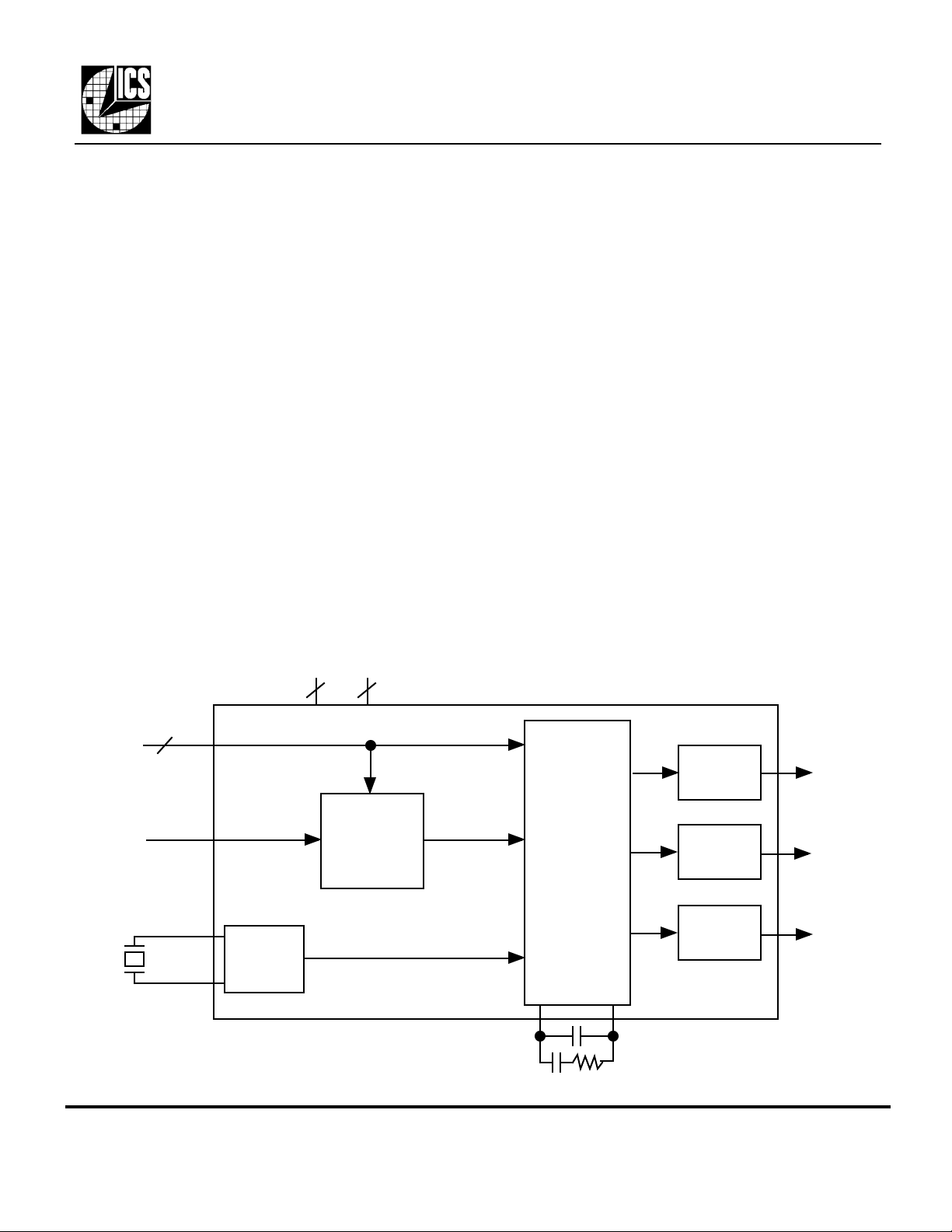
Block Diagram
VDD GND
44
Features
• Packaged in 20 pin SOIC
• Meets the TR62411, ETS300 011, and GR-1244
specification for MTIE, Pull-in/Hold-in Range,
Phase Transients, and Jitter Generation for
Stratum 3, 4, and 4E
• Accepts multiple inputs: 8 kHz backplane clock or
Loop Timing frequencies
• Locks to 8 kHz ±100 ppm (External mode)
• Exact internal ratios eliminate the need for external
dividers
• Zero ppm synthesis error in all output clocks.
• Output clock rates include T1, E1, T3, E3, and
OC3÷8
• 5 V ±5% operation
• Offered in Commercial and Industrial temperature
versions
FS3:0
Clock
Input
Reference
Crystal
MDS 2049-01 J 1 Revision 040601
Integrated Circuit Systems, Inc. • 525 Race Street • San Jose • CA • 95126 • (408)295-9800tel •www.icst.com
4
Output
Buffer
Output
Buffer
Output
Buffer
CLK1
CLK2
8 kHz
X1
X2
Crystal
Oscillator
External/
Loop
Timing
Mux
CAP1
PLL
Clock
Synthesis,
Control, and
Jitter
Attenuation
Circuitry
CAP2
Page 2
MK2049-01
Communications Clock PLL
Pin Assignment
FS1 FS0
X2
X1
VDD
VDD
VDD
GND
CLK2
CLK1
8K
1
2
3
4
5
6
7
8
9
10
20 pin (300 mil) SOIC
20
19
18
17
16
15
14
13
12
11
GND
CAP2
GND
CAP1
VDD
GND
ICLK
FS3
FS2
Output Decoding Table – External Mode (MHz)
Input FS3 FS2 FS1 FS0 CLK1 CLK2 Crystal
8 kHz 0 0 0 0 1.544 3.088 12.288
8 kHz 0 0 0 1 2.048 4.096 12.288
8 kHz 0 0 1 0 22.368 44.736 12.288
8 kHz 0 0 1 1 17.184 34.368 12.288
8 kHz 0 1 1 1 19.44 38.88 12.96
Output Decoding Table – Loop Timing Mode (MHz)
Input FS3 FS2 FS1 FS0 CLK1 CLK2 Crystal
1.544 1 0 0 0 1.544 3.088 12.288
2.048 1 0 0 1 2.048 4.096 12.288
44.736 1 0 1 0 22.368 44.736 12.288
34.368 1 0 1 1 17.184 34.368 12.288
• 0 = connect directly to ground, 1 = connect directly to VDD.
• Crystal is applied to pins 2 and 3; clock input is applied to pin 13.
Pin Descriptions
Number Name Type Description
1 FS1 I Frequency Select 1. Determines CLK input/outputs per tables above.
2 X2 O Crystal conection. Connect to a 12.288 MHz or 12.96 MHz crystal.
3 X1 I Crystal conection. Connect to a 12.288 MHz or 12.96 MHz crystal.
4 VDD P Connect to +5V.
5 VDD P Connect to +5V.
6 VDD P Connect to +5V.
7 GND P Connect to ground.
8 CLK2 O Clock 2 output determined by status of FS3:0 per tables above.
9 CLK1 O Clock 1 output determined by status of FS3:0 per tables above. CLK2 divided by 2.
10 8K O Recovered 8 kHz clock output. On External mode only.
11 FS2 I Frequency Select 2. Determines CLK input/outputs per tables above.
12 FS3 I Frequency Select 3. Determines CLK input/outputs per tables above.
13 ICLK I Input clock connection. Connect to 8 kHz backplane or to Loop Timing clock.
14 GND P Connect to ground.
15 VDD P Connect to +5V.
16 CAP1 LF Connect a 0.030 µF ceramic capacitor and a 7.5 MΩ resistor in series between this pin and CAP2.
17 GND P Connect to ground.
18 CAP2 LF Connect a 0.030 µF ceramic capacitor and a 7.5 MΩ resistor in series between this pin and CAP1.
19 GND P Connect to ground.
20 FS0 I Frequency Select 0. Determines CLK input/outputs per tables above.
Type: I = Input, O = output, P = power supply connection, LF = loop filter connection
MDS 2049-01 J 2 Revision 040601
Integrated Circuit Systems, Inc. • 525 Race Street • San Jose • CA • 95126 • (408)295-9800tel •www.icst.com
Page 3
MK2049-01
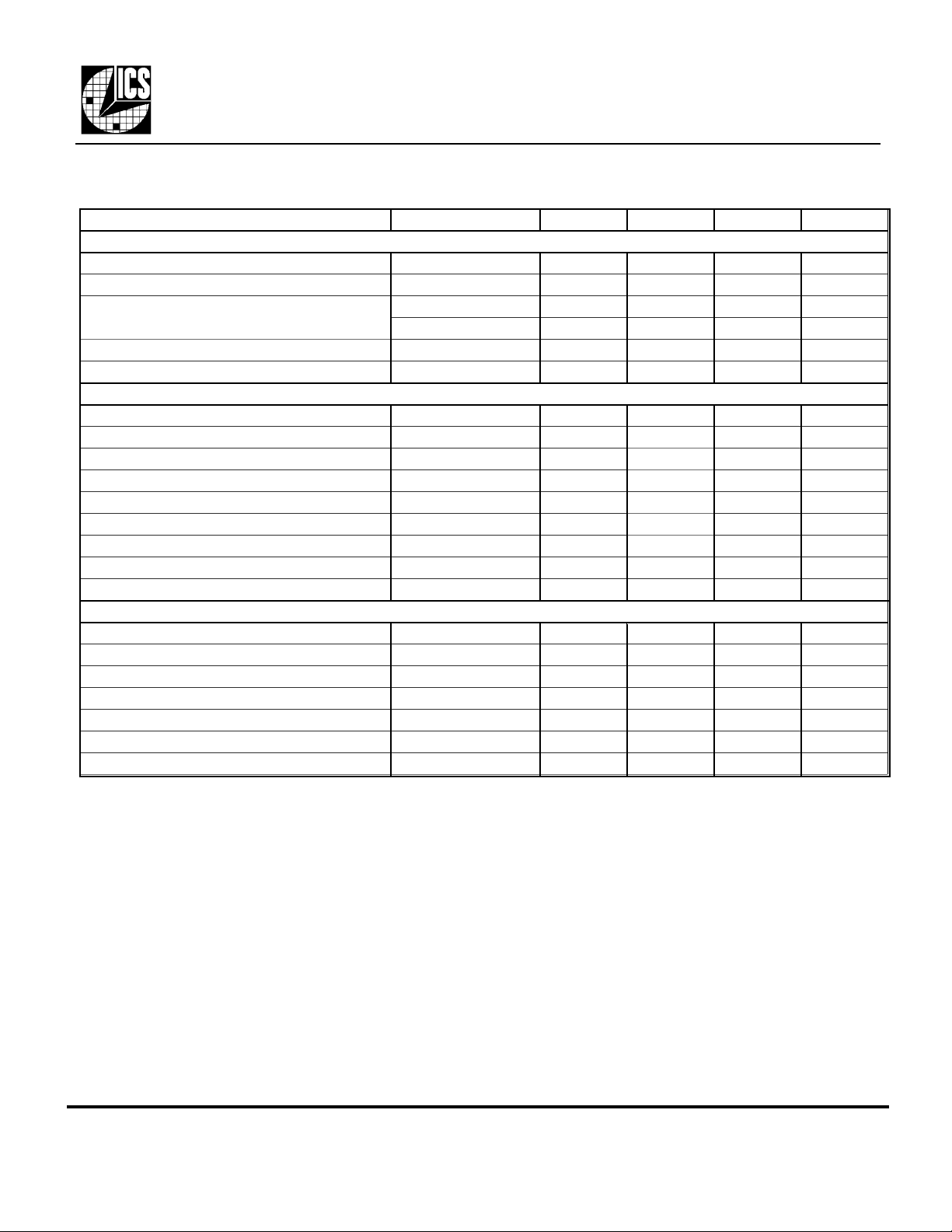
ABSOLUTE MAXIMUM RATINGS (Note 1)
DC CHARACTERISTICS (VDD = 5 V unless noted)
AC CHARACTERISTICS (VDD = 5 V unless noted)
Communications Clock PLL
Electrical Specifications
Parameter Conditions Minimum Typical Maximum Units
Supply Voltage, VDD Referenced to GND 7 V
Inputs and Clock Outputs -0.5 VDD+0.5 V
Ambient Operating Temperature 0 70 °C
MK2049-01SI only -40 85 °C
Soldering Temperature Max of 10 seconds 250 °C
Storage Temperature -65 150 °C
Operating Voltage, VDD 4.75 5.25 V
Input High Voltage, VIH 2 V
Input Low Voltage, VIL 0.8 V
Output High Voltage IOH=-4mA VDD-0.4 V
Output High Voltage IOH=-25mA 2.4 V
Output Low Voltage IOL=25mA 0.4 V
Operating Supply Current, IDD No Load, VDD=5.0V 20 mA
Short Circuit Current Each output ±100 mA
Input Capacitance, FS3:0 7 pF
Input Frequency, External Mode ICLK 8.0000 kHz
Input Crystal Frequency X1, X2 12.2880 MHz
Input Crystal Frequency X1, X2. Selection 0111 12.9600 MHz
Output Clock Rise Time 0.8 to 2.0V 1.5 ns
Output Clock Fall Time 2.0 to 0.8V 1.5 ns
Output Clock Duty Cycle, High Time At VDD/2 40 49 to 51 60 %
Actual mean frequency error versus target Any clock selection 0 0 ppm
Notes:
1. Stresses beyond those listed under Absolute Maximum Ratings could cause permanent damage to the device. Prolonged exposure
to levels above the operating limits but below the Absolute Maximums may affect device reliability.
MDS 2049-01 J 3 Revision 040601
Integrated Circuit Systems, Inc. • 525 Race Street • San Jose • CA • 95126 • (408)295-9800tel •www.icst.com
Page 4

MK2049-01
Communications Clock PLL
OPERATING MODES
The MK2049-01 has two operating modes: External and Loop Timing. Although both modes use an input
clock to generate various output clocks, there are important differences in their input requirements.
External Mode
The MK2049-01 accepts an external 8 kHz clock and will produce a number of common communication
clock frequencies. The 8 kHz input clock does not need to have a 50% duty cycle; a “high” or “on” pulse as
narrow as 10 ns is acceptable.
Loop Timing Mode
This mode can be used to remove the jitter from standard high-frequency communication clocks. For T1
and E1 inputs, the CLK1 output will be the same as the input frequency, with CLK2 at twice the input
frequency. For T3 and E3 inputs, CLK1 will be 1/2 the input frequency and CLK2 will be the same as the
input frequency.
FREQUENCY LOCKING TO THE INPUT
In both modes, the output clocks are frequency-locked to the input. The output will remain at the specified
output frequency as long as the combined variation of the input frequency and the crystal does not exceed
100 ppm. For example, if the crystal can vary ±40 ppm (initial accuracy + temperature + aging), then the
input frequency can vary by up to 60 ppm and still have the output clock remain frequency-locked.
INPUT AND OUTPUT SYNCHRONIZATION
The rising edges of CLK1 and CLK2 do not have a fixed phase alignment with the rising edge of ICLK.
Each time the device is powered-up, the phase relationship could change. Refer to one of the other
MK2049 versions (e.g., MK2049-02, -03, -34) if input-output phase alignment is important in your
application.
MDS 2049-01 J 4 Revision 040601
Integrated Circuit Systems, Inc. • 525 Race Street • San Jose • CA • 95126 • (408)295-9800tel •www.icst.com
Page 5

MK2049-01
Communications Clock PLL
LAYOUT AND EXTERNAL COMPONENTS
The MK2049-01 requires a minimum number of external components for proper operation. Decoupling
capacitors of 0.01µF must be connected between VDD and GND pins close to the chip (especially pins 4
and 7, 15 and 17), and 33 Ω series terminating resistors should be used on clock outputs with traces longer
than 1 inch (assuming 50 Ω traces). The loop filter components should be connected as close to the chip as
possible. Refer to the next section for more information.
PC Board Layout
A proper board layout is critical to the successful use of the MK2049. In particular, the CAP1 and CAP2 pins
are very sensitive to noise and leakage (CAP2 at pin 18 is the most sensitive). Traces must be as short as
possible and the two capacitors and resistor must be mounted next to the device as shown below. The
capacitor shown between pins 15 and 17, and the one between pins 5 and 7 are the power supply decoupling
capacitors. The high frequency output clocks on pins 8 and 9 should have a series termination of 33 Ω
connected close to the pin. Additional improvements will come from keeping all components on the same
side of the board, minimizing vias through other signal layers, and routing other signals away from the
MK2049. You may also refer to MAN05 for additional suggestions on layout of the crystal section.
The crystal traces should include pads for small capacitors from X1 and X2 to ground; these are used to
adjust the stray capacitance of the board to match the crystal load capacitance. The typical telecom reference
frequency is accurate to much less than 1 ppm, so the MK2049 may lock and run properly even if the board
capacitance is not adjusted with these fixed capacitors. However, ICS MicroClock recommends that the
adjustment capacitors be included to minimize the effects of variation in individual crystals, temperature,
and aging. The value of these capacitors (typically 0-4 pF) is determined once for a given board layout,
using the procedure described later in this section, titled “Determining the Crystal Frequency Adjustment
Capacitors”.
Cutout in ground and power plane.
Optional;
see text
cap
G
cap
V
cap
resist.
resist.
Route all traces away from this area.
1
2
3
4
5
6
7
8
9
20
19
18
17
16
15
14
13
12
cap
G
V
cap
resist.
cap
=connect to VDD
V
=connect to GND
G
1110
Figure 1. MK2049-01 Layout Example
MDS 2049-01 J 5 Revision 040601
Integrated Circuit Systems, Inc. • 525 Race Street • San Jose • CA • 95126 • (408)295-9800tel •www.icst.com
Page 6

MK2049-01
Communications Clock PLL
LAYOUT AND EXTERNAL COMPONENTS (continued)
Loop Filter Components
The external loop filter should be connected between CAP1 and CAP2 as shown in Figure 2 below, and as
close to the chip as possible. Be sure to follow the recommendations on capacitor types described on page 6.
CAP2
1.5 nF
CAP1
Figure 2. Loop Filter component values for most configurations
Typical component values are shown. Contact the ICS MicroClock applications
department at (408)297-1201 for the recommended values for your application.
7.5 MΩ
0.030 µF
Crystal Operation
The MK2049 operates by phase locking the input signal to a VCXO which consists of the special
recommended crystal and the integrated VCXO oscillator circuit on the MK2049. To achieve the best
performance and reliability, the layout guidelines shown on the previous page must be closely followed.
The frequency of oscillation of a quartz crystal is determined by its cut and by the load capacitors connected
to it. The MK2049 has variable load capacitors on-chip which “pull”, or change the frequency of the crystal.
External stray capacitance must be kept to a minimum to ensure maximum pullability of the crystal. To
achieve this, the layout should use short traces between the MK2049 and the crystal.
MDS 2049-01 J 6 Revision 040601
Integrated Circuit Systems, Inc. • 525 Race Street • San Jose • CA • 95126 • (408)295-9800tel •www.icst.com
Page 7

Communications Clock PLL
LAYOUT AND EXTERNAL COMPONENTS (continued)
Crystal Specifications
Parameter Minimum Typical Maximum Units
Operating Temperature Range 0 25 70 °C
Initial Accuracy at 25 C -20 20 ppm
Temperature stability -30 30 ppm
Aging, first year -5 5 ppm
Aging, 10 years -20 20 ppm
Load Capacitance Note 1
Shunt Capacitance, C0 7 pF
Motional Capacitance, C1 none none pF
C0/C1 ratio 250 none
Equivalent Series Resistance 35 Ohms
*This ratio decreases for lower crystal frequencies.
Note 1: Nominal crystal load capacitance specification varies with frequency.
Contact the ICS MicroClock applications department at (408)297-1201.
Note 2: The third overtone mode of the crystal and all spurs must be >200 ppm
away from 3x the fundamental resonance shown in the table below.
MK2049-01
For recommended crystal devices, please contact the ICS MicroClock application department
at 408-297-1201.
MDS 2049-01 J 7 Revision 040601
Integrated Circuit Systems, Inc. • 525 Race Street • San Jose • CA • 95126 • (408)295-9800tel •www.icst.com
Page 8

MK2049-01
Communications Clock PLL
LAYOUT AND EXTERNAL COMPONENTS (continued)
Determining the Crystal Frequency Adjustment Capacitors
To determine the crystal adjustment capacitor values, you will need a PC board of your final layout, a
frequency counter capable of less than 1 ppm resolution and accuracy, two power supplies, and some samples
of the crystals which you plan to use in production, along with measured initial accuracy for each crystal at
the specified load capacitance, CL .
To determine the value of the crystal capacitors:
1. Connect VDD of the MK2049 to 5.0 V. Connect pin 18 of the MK2049 to the second power supply.
Adjust the voltage on pin 18 to 0.0 V. Measure and record the frequency of the CLK1 or CLK2 output .
2. Adjust the voltage on pin 18 to 3.0 V. Measure and record the frequency of the same output.
To calculate the centering error:
(f
Centering
error
= 10
- f
3.0V
6
target
) + (f
f
target
0.0V
- f
target
)
error
-
xtal
Where f
= 44.736000 MHz, for example, and error
target
= actual initial accuracy (in ppm) of the
xtal
crystal being measured.
If the centering error is less than ±15 ppm, no adjustment is needed. If the centering error is more than
15 ppm negative, the PC board has too much stray capacitance and will need to be redone with a new layout
to reduce stray capacitance. (The crystal may be re-specified to a lower load capacitance instead. Contact ICS
MicroClock for details.) If the centering error is more than 15 ppm positive, add identical fixed centering
capacitors from each crystal pin to ground. The value for each of these caps (in pF) is given by:
External Capacitor = 2*(centering error)/(trim sensitivity)
Trim sensitivity is a parameter which can be supplied by your crystal vendor. If you do not know the value,
assume it is 30 ppm/pF. After any changes, repeat the measurement to verify that the remaining error is
acceptably low (less than ±15 ppm).
The MicroClock Applications department can perform this procedure on your board. Call us at 408-2959800, and we will arrange for you to send us a PC board (stuffed or unstuffed) and one of your crystals. We
will calculate the value of capacitors needed.
MDS 2049-01 J 8 Revision 040601
Integrated Circuit Systems, Inc. • 525 Race Street • San Jose • CA • 95126 • (408)295-9800tel •www.icst.com
Page 9

Communications Clock PLL
Measured Jitter Output (UIp-p)
Measured Jitter Output (UIp-p)
Input Jitter
Modulation Input Jitter Output Jitter Jitter
Frequency Magnitude Magnitude Attenuation
(Hz) (UIp-p) (UIp-p) (dB)
10 10 1.07 19.41
20 10 0.56 25.04
40 10 0.36 28.87
100 10 0.147 36.65
400 10 0.037 48.64
1000 10 0.016 55.92
2000 10 0.01 60.00
4000 10 0.01 60.00
8000 10 0.01 60.00
10000 10 0.01 60.00
16000 7.75 0.01 57.79
32000 3.98 0.01 52.00
64000 1.74 0.01 44.81
MK2049-01
Table 1. Jitter results for a T1 (1.544 MHz) reference frequency, as
measured on the HP3785B (10 Hz - 40 kHz output filter).
Input Jitter
Modulation Input Jitter Output Jitter Jitter
Frequency Magnitude Magnitude Attenuation
(Hz) (UIp-p) (UIp-p) (dB)
100 10.5 0.071 43.4
400 10.5 0.07 43.52
1000 10.5 0.144 37.26
2000 10.5 0.12 38.84
4000 10.5 0.08 42.36
8000 10.5 0.07 43.52
10000 10.5 0.066 44.03
16000 10.5 0.065 44.17
32000 10.5 0.06 44.86
64000 10.5 0.06 44.86
128000 10.5 0.058 45.16
192000 10.5 0.06 44.86
256000 10.5 0.062 44.58
Table 2. Jitter results for a T3 (44.736 MHz) reference frequency, as
measured on the HP3785B (10 Hz -1.1 MHz output filter).
MDS 2049-01 J 9 Revision 040601
Integrated Circuit Systems, Inc. • 525 Race Street • San Jose • CA • 95126 • (408)295-9800tel •www.icst.com
Page 10

Communications Clock PLL
Measured Jitter Output (UIp-p)
Measured Jitter Output (UIp-p)
Input Jitter
Modulation Input Jitter Output Jitter Jitter
Frequency Magnitude Magnitude Attenuation
(Hz) (UIp-p) (UIp-p) (dB)
20 1.5 0.018 38.42
50 1.5 0.014 40.60
100 1.5 0.01 43.52
200 1.5 0.01 43.52
500 1.5 0.007 46.62
1000 1.5 0.006 47.96
2000 1.5 0.006 47.96
5000 0.72 0.006 41.58
10000 0.36 0.006 35.56
15000 0.24 0.006 32.04
25000 0.20 0.006 30.46
50000 0.20 0.006 30.46
75000 0.20 0.006 30.46
MK2049-01
Table 3. Jitter results for an E1 (2.048 MHz) reference frequency, as
measured on the HP3785A (100 Hz -800 kHz output filter).
Input Jitter
Modulation Input Jitter Output Jitter Jitter
Frequency Magnitude Magnitude Attenuation
(Hz) (UIp-p) (UIp-p) (dB)
100 1.5 0.113 22.46
200 1.5 0.094 24.06
500 1.5 0.077 25.79
1000 1.5 0.069 26.74
2000 1.5 0.07 26.62
5000 0.72 0.068 20.5
10000 0.36 0.007 34.22
15000 0.24 0.007 30.7
25000 0.2 0.007 29.12
50000 0.2 0.007 29.12
75000 0.2 0.007 29.12
100000 0.2 0.007 29.12
Table 4. Jitter results for an E3 (34.368 MHz) reference frequency, as
measured on the HP3785A (100 Hz - 800 kHz output filter).
MDS 2049-01 J 10 Revision 040601
Integrated Circuit Systems, Inc. • 525 Race Street • San Jose • CA • 95126 • (408)295-9800tel •www.icst.com
Page 11

Communications Clock PLL
Inches
Millimeters
Package Outline and Package Dimensions
(For current dimensional specifications, see JEDEC Publication No. 95.)
20 pin SOIC
Symbol Min Max Min Max
A -- 0.104 -- 2.65
A1 0.0040 -- 0.10 --
E H
INDEX
AREA
1 2
h x 45°
D
B 0.013 0.020 0.33 0.51
C 0.007 0.013 0.18 0.33
D 0.496 0.512 12.60 13.00
E 0.291 0.299 7.40 7.60
e
H 0.394 0.419 10.01 10.64
h 0.01 0.029 0.25 0.74
L 0.016 0.050 0.41 1.27
MK2049-01
A1 C
A
e
B
L
Ordering Information
Part/Order Number Marking Package Temperature
MK2049-01S MK2049-01S 20 pin SOIC 0 to 70 °C
MK2049-01STR MK2049-01S Add Tape & Reel 0 to 70 °C
MK2049-01SI MK2049-01SI 20 pin SOIC -40 to 85 °C
MK2049-01SITR MK2049-01SI Add Tape & Reel -40 to 85 °C
While the information presented herein has been checked for both accuracy and reliability, ICS/MicroClock assumes no responsibility for either its use or for the infringement of
any patents or other rights of third parties, which would result from its use. No other circuits, patents, or licenses are implied. This product is intended for use in normal
commercial applications. Any other applications such as those requiring extended temperature range, high reliability, or other extraordinary environmental requirements are not
recommended without additional processing by ICS/MicroClock. ICS/MicroClock reserves the right to change any circuitry or specifications without notice. ICS/MicroClock
does not authorize or warrant any ICS/MicroClock product for use in life support devices or critical medical instruments.
MDS 2049-01 J 11 Revision 040601
Integrated Circuit Systems, Inc. • 525 Race Street • San Jose • CA • 95126 • (408)295-9800tel •www.icst.com
 Loading...