

Page 1
ADVANCE INFORMATION
MK2042-01
ICRO
C
LOCK
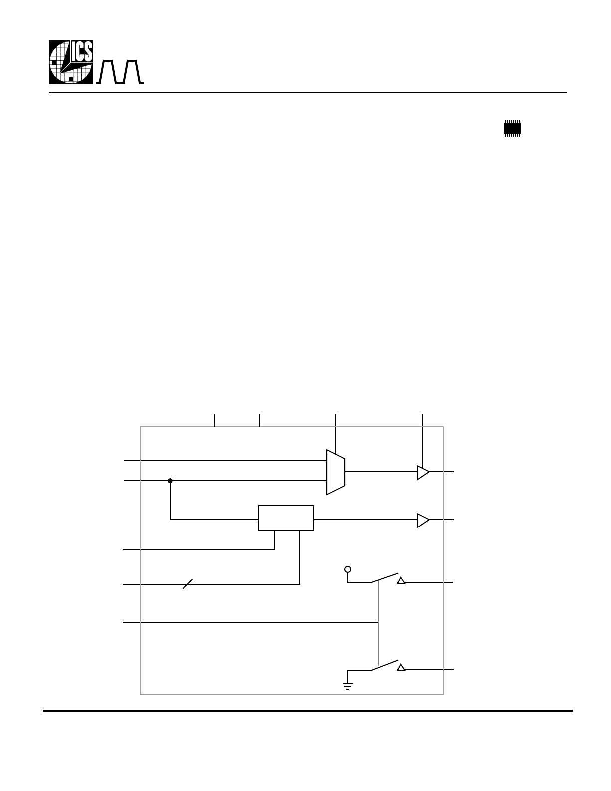
Description
The MK2042-01 is designed to switch between
two clock sources. The switching can be externally
controlled by an input pin or configured to switch
automatically if the primary input clock stops.
The part also provides clock detection by reporting
when the primary input clock has stopped.
The MK2042-01 is optimized for use with our
MK2049 family of Communication Clock
Synthesizers. When used together, the
MK2042-01 and MK2049 provide a complete
system for switching to an alternate source when
the primary clock is lost, or for maintaining a
stable frequency on the MK2049 output.
For switching between clock sources with no
output glitches or short pulses, use the ICS580 or
ICS581 multiplexers.
Communications Clock Monitor
Features
• Packaged in 16 pin SOIC
• User controlled or automatic switching
• Clock detect feature
• Does not add jitter or phase noise to the clock
• Ideal for systems with backup or redundant clocks
• Selectable timeouts for clock loss detection
• Accepts input frequencies from 0 Hz to 160 MHz
• Works with all MK2049-xx to provide enhanced
operation
• 3.3 V or 5 V operation
Block Diagram
INB
INA
REFIN
S2:S0
CENTER
VDD GND
3
Clock Loss
Detector
OESELB
CLKOUT
NO_INA
VDD
HIGH
LOW
GND
MDS 2042-01 1 Revision 102600 Printed 11/15/00
Integrated Circuit Systems, Inc. • 525 Race Street • San Jose • CA • 95126 • (408)295-9800tel• www.icst.com
Page 2
ADVANCE INFORMATION
MK2042-01
ICRO
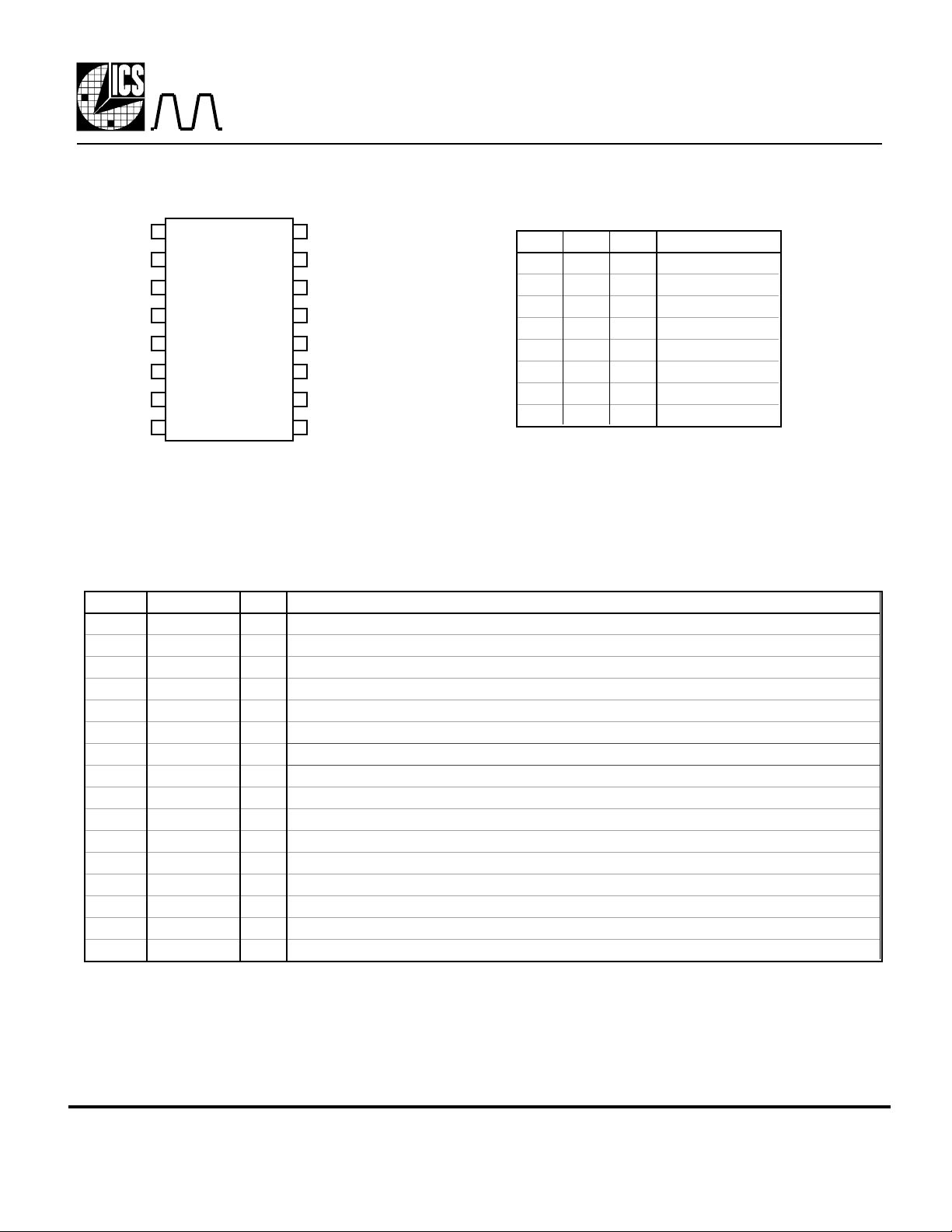
Pin Assignment
S0 OE
S1
S2
INB
INA
GND
SELB
Pin Descriptions
1
2
3
4
5
6
7
8
16 pin (150 mil) SOIC
16
15
14
13
12
11
10
9
C
LOCK
VDD
CLKOUT
NO_INA
HIGH
LOW
GND
CENTERREFIN
Communications Clock Monitor
Clock Loss Detector Settings
S2 S1 S0 Nominal Count
0 0 0 34
0 0 1 18
0 1 0 130
0 1 1 66
1 0 0 10
1 0 1 6
1 1 0 2
1 1 1 2
Due to the possible phase differences between
the REFIN clock and the INA clock, the
Nominal Count has a tolerance of -0/+1
REFIN clock edges.
Number Name Type Description
1 S0 I Clock Count Select 0. Determines allowed number of missing clock edges per table above.
2 S1 I Clock Count Select 1. Determines allowed number of missing clock edges per table above.
3 S2 I Clock Count Select 2. Determines allowed number of missing clock edges per table above.
4 INB I Input Clock B.
5 INA I Input Clock A.
6 GND P Connect to ground.
7 SELB I Mux select. Selects INB when high.
8 REFIN I Reference Clock Input.
9 CENTER I Enables HIGH and LOW pins when high.
10 GND P Connect to ground.
11 LOW O Sets low end of centering range.
12 HIGH O Sets high end of centering range.
13 NO_INA O Goes high when clock on INA stops.
14 CLKOUT O Clock output.
15 VDD P Connect to +3.3 V or +5 V.
16 OE I Output Enable. Tri-states CLKOUT when low.
Type: I = Input, O = output, P = power supply connection
All inputs have an internal pull-up.
MDS 2042-01 2 Revision 102600 Printed 11/15/00
Integrated Circuit Systems, Inc. • 525 Race Street • San Jose • CA • 95126 • (408)295-9800tel• www.icst.com
Page 3

ADVANCE INFORMATION
ABSOLUTE MAXIMUM RATINGS (Note 1)
DC CHARACTERISTICS (VDD = 3.3 V unless noted)
AC CHARACTERISTICS (VDD = 3.3 V unless noted)
MK2042-01
ICRO
C
LOCK
Communications Clock Monitor
Electrical Specifications
Parameter Conditions Minimum Typical Maximum Units
Supply Voltage, VDD Referenced to GND 7 V
Inputs and Clock Outputs -0.5 VDD+0.5 V
Ambient Operating Temperature -40 85 °C
Soldering Temperature Max of 10 seconds 250 °C
Storage Temperature -65 150 °C
Operating Voltage, VDD 3.14 5.25 V
Input High Voltage, VIH (Note 2) INA, INB (VDD/2)+1 V
Input Low Voltage, VIL (Note 2) INA, INB (VDD/2)-1 V
Input High Voltage, VIH 2 V
Input Low Voltage, VIL 0.8 V
Output High Voltage, VOH, CMOS level IOH=-4 mA VDD-0.4 V
Output High Voltage, VOH IOH=-8 mA 2.4 V
Output Low Voltage IOL=8 mA 0.4 V
Operating Supply Current, IDD No Load, VDD=3.3 V 5 mA
Short Circuit Current Each output ±50 mA
Input Capacitance 7 pF
Input Frequency, External Mode INA, INB, REFIN 0 100 MHz
Input Clock Pulse Width 4 ns
CLKOUT Settling Time After SELB change 1 ms
Output Clock Rise Time 0.8 to 2.0 V 1.5 ns
Output Clock Fall Time 2.0 to 0.8 V 1.5 ns
Output Clock Duty Cycle, High Time At VDD/2 40 60 %
Notes:
1. Stresses beyond those listed under Absolute Maximum Ratings could cause permanent damage to the device. Prolonged exposure
to levels above the operating limits but below the Absolute Maximums may affect device reliability.
2. Switching occurs nominally at VDD/2.
3: The phase relationship between input and output clocks can change at power up or when switching between INA and INB.
EXTERNAL COMPONENT SELECTION
The MK2042-01 requires a minimum number of external components for proper operation. A decoupling
capacitor of 0.01µF must be connected between VDD and GND, pins 15 and 10. This capacitor should be
as close to the chip as possible. A series termination resistor of 33 Ω may be used on CLKOUT with traces
longer than 1 inch (assuming 50 Ω traces). In applications where the HIGH and LOW outputs are
connected to the MK2049-xx, 10 kΩ resistors should be used on each of those outputs.
MDS 2042-01 3 Revision 102600 Printed 11/15/00
Integrated Circuit Systems, Inc. • 525 Race Street • San Jose • CA • 95126 • (408)295-9800tel• www.icst.com
Page 4

ADVANCE INFORMATION
MK2042-01
ICRO
C
LOCK
Communications Clock Monitor
DETECTING CLOCK LOSS
The MK2042-01 internal Clock Loss Detector compares the REFIN clock to the INA clock to determine
when the INA clock is no longer present. During normal operation, the Detector is reset with each rising
edge of the INA clock, and the NO_INA output will remain low. In a fault condition where the INA
clock is removed, the Detector will use the REFIN clock to wait the pre-determined number of REFIN
clock pulses (set by S2:S0 per the table on page 2), and will then force the NO_INA output to a high level.
The NO_INA signal can be used to notify the system that the input clock has been lost, or it can provide
automatic switchover to INB. Automatic switchover to INB is achieved by connecting NO_INA to the
SELB input, as illustrated in Figure 1. In this case the MK2042-01 will automatically switch CLKOUT to
the INB input when the loss of INA is detected. With this configuration, when INA becomes active again,
NO_INA will go low and the MK2042-01 will switch CLKOUT to INA. Since the Clock Loss Detector
will set NO_INA low as soon as an INA clock edge occurs, sporadic edges on INA could cause CLKOUT
to switch unpredictably between INA and INB. Because of this, external system control of SELB is best in
cases where the INA clock is sporadic.
Note that proper operation of the Clock Loss Detector requires that there always be a clock on REFIN.
The REFIN clock does not need to be the same frequency as the INA clock. Because the REFIN clock and
the INA clock are asynchronous, the Clock Loss Detector Count shown in the table on page 2 has a
tolerance of -0/+1 REFIN clock edges.
MDS 2042-01 4 Revision 102600 Printed 11/15/00
Integrated Circuit Systems, Inc. • 525 Race Street • San Jose • CA • 95126 • (408)295-9800tel• www.icst.com
Page 5

ADVANCE INFORMATION
MK2042-01
ICRO
C
LOCK
S0
S1
S2
INB
INA
GND
SELB
REFIN
Communications Clock Monitor
VDD
OE
VDD
0.01µF
CLKOUT
NO_INA
10 kΩ
HIGH
LOW
10 kΩ
GND
CENTER
8 kHz clock
from network
FS1
X2
X1
VDD
FCAP
VDD
GND
FS0
RES
CAP2
GND
CAP1
VDD
GND
In this configuration, the output
CLK
CLK/2
8K
(Not all connections for
MK2049-34 are shown.)
ICLK
FS3
FS2
frequency of the MK2049-34
will be held at the nominal
value after missing 2 cycles of
the 8 kHz network clock.
Figure 1. Typical Application of MK2042-01 With MK2049-34
MDS 2042-01 5 Revision 102600 Printed 11/15/00
Integrated Circuit Systems, Inc. • 525 Race Street • San Jose • CA • 95126 • (408)295-9800tel• www.icst.com
Page 6

ADVANCE INFORMATION
Inches
Millimeters
MK2042-01
ICRO
C
LOCK
Communications Clock Monitor
Package Outline and Package Dimensions
(For current dimensional specifications, see JEDEC Publication No. 95.)
16 pin SOIC narrow
Symbol Min Max Min Max
A 0.0532 0.0688 1.35 1.75
A1
E H
INDEX
AREA
1 2
h x 45°
D
B 0.0130 0.0200 0.33 0.51
C
D 0.3859 0.3937 9.80 10.00
E 0.1497 0.1574 3.80 4.00
e
H 0.2284 0.2440 5.80 6.20
h 0.0099 0.0195 0.25 0.50
L 0.0160 0.0500 0.41 1.27
0.0040 0.0098 0.10 0.24
0.0075 0.0098 0.19 0.24
A1 C
A
e
B
L
Ordering Information
Part/Order Number Marking Package Temperature
MK2042-01SI MK2042-01SI 20 pin SOIC -40 to 85 °C
MK2042-01SITR MK2042-01SI Add Tape & Reel -40 to 85 °C
While the information presented herein has been checked for both accuracy and reliability, Integrated Circuit Systems (ICS) assumes no responsibility for either its use or for the
infringement of any patents or other rights of third parties, which would result from its use. No other circuits, patents, or licenses are implied. This product is intended for use in
normal commercial applications. Any other applications such as those requiring extended temperature range, high reliability, or other extraordinary environmental requirements
are not recommended without additional processing by ICS. ICS reserves the right to change any circuitry or specifications without notice. ICS does not authorize or warrant any
ICS product for use in life support devices or critical medical instruments.
MDS 2042-01 6 Revision 102600 Printed 11/15/00
Integrated Circuit Systems, Inc. • 525 Race Street • San Jose • CA • 95126 • (408)295-9800tel• www.icst.com
 Loading...