

Page 1
MK1714-02
Spread Spectrum Multiplier Clock
Description
The MK1714-02 is a low cost, high performance
clock synthesizer with selectable multipliers and
spread amounts (percentages), designed to
generate high frequency clocks with low EMI.
Using analog/digital Phase-Locked Loop (PLL)
techniques, the device accepts an inexpensive,
fundamental mode, parallel resonant crystal, or a
clock input to produce a spread, or dithered,
output, thereby reducing the frequency amplitude
peaks by several dB. The OE pin puts both outputs
into a high impedance state for board level testing.
The PD# pin powers down the entire chip, and the
outputs are held low.
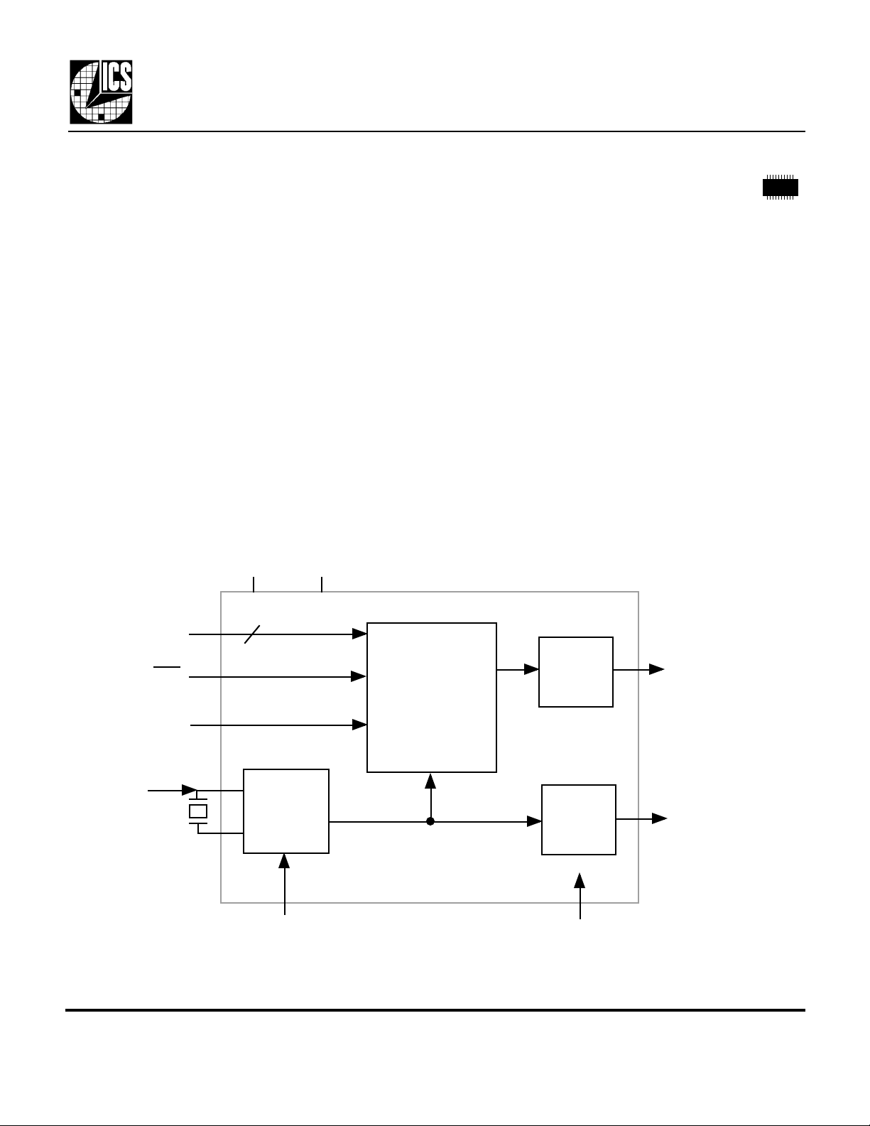
Block Diagram
VDD GND
Features
• Packaged in 20 pin tiny SSOP (QSOP)
• Operating VDD of 3.3 V or 5 V
• Multiplier modes of x1, x2, x3, x4, x5, and x6
• Inexpensive 10-25 MHz crystal, or clock input
• OE pin tri-states the outputs for testing
• Power down pin stops the outputs low
• Selectable frequency spread
• Spread can be turned on or off
• Duty cycle of 40/60
• Advanced, low power CMOS process
• Industrial temperature range available
S4:0
PD
Low EMI
Enable
Input crystal
or clock
MDS 1714-02 C 1 Revision 120400
Integrated Circuit Systems, Inc. • 525 Race Street • San Jose •CA•95126• (408) 295-9800tel • www.icst.com
X1
X2
5
Crystal
Oscillator
XSEL
PLL Clock
Multiplier and
Spread
Spectrum
Circuitry
Output
Buffer
Output
Buffer
OE (both outputs)
Clock Out
REF
Page 2
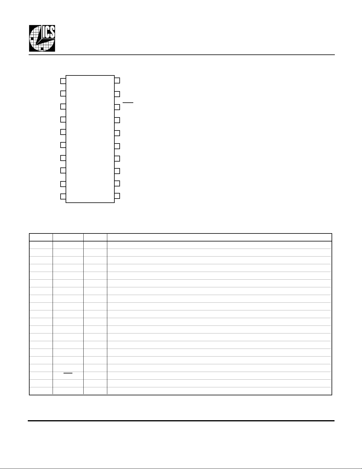
Pin Assignment
MK1714-02
Spread Spectrum Multiplier Clock
X2
X1/ICLK
VDD
VDD
S4
S3
GND
GND
S2
CLK
1
2
3
4
5
6
7
8
9
10
16
15
14
13
12
11
20
19
18
17
REF
OE
PD
GND
S0
NC
S1
GND
LEE
XSEL
20 pin.150 mil SSOP (QSOP)
Pin Descriptions
Pin # Name Type Description
1 X2 XO Crystal connection. Connect to parallel mode crystal. Leave open for clock.
2 X1/ICLK XI Crystal connection. Connect to parallel mode crystal, or clock.
3 VDD P Connect to VDD. Must be same value as other VDD.
4 VDD P Connect to VDD. Must be same value as other VDD. Decouple with pin 7.
5 S4 I(D) Select pin number 4. Determines multiplier and spread amount per table on following page.
6 S3 I Select pin number 3. Determines multiplier and spread amount per table on following page.
7
8 GND P Connect to ground.
9 S2 I Select pin number 2. Determines multiplier and spread amount per table on following page.
10 CLK O Clock output which depends on the input, multiplier and spread amount per table on page 3.
11 XSEL I Connect to VDD for crystal input, or GND for CLK input.
12 LEE I Low EMI Enable. Turns on the Spread spectrum when high.
13 GND P Connect to ground.
14
15 NC - No Connect.
16 S0 I Select pin number 0. Determines multiplier and spread amount per table on following page.
17 GND P Connect to ground.
18 PD I Power Down. Turns off the chip when low. Outputs stop low.
19 OE I Output Enable. Tri-states all outputs when low.
20 REF O Reference clock output from crystal oscillator.
GND P Connect to ground.
S1 I Select pin number 1. Determines multiplier and spread amount per table on following page.
Key: I = Input with internal pull-up; I(D) = Input with internal pull-down; XO/XI = crystal connections;
O = output; P = power supply connection
MDS 1714-02 C 2 Revision 120400
Integrated Circuit Systems, Inc. • 525 Race Street • San Jose •CA•95126• (408) 295-9800tel • www.icst.com
Page 3

Clock Output Select Table (in MHz)
MK1714-02
Spread Spectrum Multiplier Clock
S4 S3 S2 S1 S0 Input Range Multiplier Output Range Direction Amount (%)
0 0 0 0 0 40-80 x1 40-80 C ±0.75
0 0 0 0 1 60-120 x1 60-120 DC +0.25, -0.75
0 0 0 1 0 40-80 x1 40-80 C ±1.25
0 0 0 1 1 80-150 x1 80-150 C ±0.75
0 0 1 0 0 10-30 x2 20-60 C ±0.75
0 0 1 0 1 20-60 x2 40-120 C ±0.5
0 0 1 1 0 10-25 x2 20-50 DC +0.25, -1.5
0 0 1 1 1 20-60 x2 40-120 DC +0.5, -1.0
0 1 0 0 0 20-30 x3 60-90 C ±0.5
0 1 0 0 1 40-75 x2 80-150 C ±0.75
0 1 0 1 0 40-100 x1 40-100 DC +0.25, -1.5
0 1 0 1 1 40-75 x2 80-150 DC +0.25, -1.5
0 1 1 0 0 20-40 x1 20-40 DC +0.5, -2.0
0 1 1 0 1 20-60 x1 20-60 DC +0.25, -1.5
0 1 1 1 0 10-20 x1 10-20 DC +0.5, -2.0
0 1 1 1 1 10-30 x1 10-30 DC +0.25, -1.5
1 0 0 0 0 20-37.5 x4 80-150 DC +0.25, -1.25
1 0 0 0 1 20-40 x3 60-120 DC +0.25, -1.5
1 0 0 1 0 10-30 x1 10-30 C ±0.75
1 0 0 1 1 20-30 x1 20-30 D -0.5
1 0 1 0 0 5-20 x2 10-40 DC +0.25, -2.25
1 0 1 0 1 20-50 x3 60-150 D -0.25, -2.25
1 0 1 1 0 20-37.5 x4 80-150 C ±0.75
1 0 1 1 1 80-150 x1 80-150 DC +0.25, -1.25
1 1 0 0 0 10-25 x4 40-100 C ±0.75
1 1 0 0 1 10-20 x5 50-100 C ±0.75
1 1 0 1 0 10-20 x6 60-120 C ±0.75
1 1 0 1 1 20-50 x1 20-50 C ±0.75
1 1 1 0 0 10-25 x4 40-100 DC +0.25, -1.5
1 1 1 0 1 10-20 x5 50-100 DC +0.25, -1.25
1 1 1 1 0 10-20 x6 60-120 D -1.5
1 1 1 1 1 10-30 x1 10-30 C ±0.75
3.3/5V
Both
Both
Both
Both
Both
Both
Both
Both
Both
Both
Both
Both
3.3 V
Both
Both
Both
Both
Both
Both
Both
3.3 V
Both
Both
Both
Both
Both
Both
Both
Both
Both
Both
Both
For S4:S0, 0 = connect to GND, 1 = connect to VDD.
Direction: C=Center spread, D=Down spread, DC=Down+Center spread.
Amount equals the spread amount. So for a 40 MHz output clock spread down 1%, the lowest
frequency is 39.60 MHz.
Contact ICS with your exact output frequency for details on spread direction and amount.
MDS 1714-02 C 3 Revision 120400
Integrated Circuit Systems, Inc. • 525 Race Street • San Jose •CA•95126• (408) 295-9800tel • www.icst.com
Page 4

MK1714-02
ABSOLUTE MAXIMUM RATINGS (note 1)
DC CHARACTERISTICS (VDD = 3.3V or 5V unless noted)
AC CHARACTERISTICS (VDD = 3.3V or 5V unless noted)
exposure to levels above the operating limits but below the Absolute Maximums may affect device reliability.
2. Multiplier of x1, all clocks at highest frequencies.
Spread Spectrum Multiplier Clock
Electrical Specifications
Parameter Conditions Minimum Typical Maximum Units
Supply voltage, VDD Referenced to GND 7 V
Inputs and Clock Outputs Referenced to GND -0.5 VDD+0.5 V
Ambient Operating Temperature 0 70 °C
MK1714-02RI only -40 85 °C
Soldering Temperature Max of 10 seconds 260 °C
Storage temperature -65 150 °C
Operating Voltage, VDD 3.0 5.5 V
Input High Voltage, VIH, X1/ICLK only Clock input VDD/2 + 1 VDD/2 V
Input Low Voltage, VIL, X1/ICLK only Clock input VDD/2 VDD/2 - 1 V
Input High Voltage, VIH Select inputs, OE, PD 2 V
Input Low Voltage, VIL Select inputs, OE, PD 0.8 V
Output High Voltage, VOH VDD=3.3V, IOH=-8mA 2.4 V
Output Low Voltage, VOL VDD=3.3V, IOL=8mA 0.4 V
Output High Voltage, VOH, VDD = 3.3 or 5V IOH=-8mA VDD-0.4 V
Operating Supply Current, IDD, at 5V No Load, note 2 40 mA
Operating Supply Current, IDD, at 3.3V No Load, note 2 26 mA
Short Circuit Current, VDD = 3.3 Each output ±50 mA
Input Capacitance Except X1, X2 7 pF
Internal Pull-up or Pull-down Resistor Except X1 500 kΩ
Input Crystal Frequency 10 25 MHz
Input Clock Frequency See page 3 10 150 MHz
Output Clock Rise Time 0.8 to 2.0V, no load 1.5 ns
Output Clock Fall Time 2.0 to 0.8V, no load 1.5 ns
Output Clock Duty Cycle At VDD/2 40 50 60 %
One Sigma Jitter, CLK 40 ps
Absolute Jitter, CLK ±160 ps
Notes: 1. Stresses beyond those listed under Absolute Maximum Ratings could cause permanent damage to the device. Prolonged
External Components
The MK1714 requires a minimum number of external components for proper operation. Decoupling
capacitors of 0.01µF should be connected between VDD and GND (on pins 4 and 7), as close to the chip
as possible. A series termination resistor of 33 Ω may be used for each clock output. The crystal must be
connected as close to the chip as possible. The crystal should be a fundamental mode and parallel resonant.
If accurate tuning is required, crystal capacitors should be connected from pins X1 to ground and X2 to
ground. The value of these capacitors is given by the following equation, where CL is the crystal load
capacitance: Crystal caps (pF) = (CL-6) x 2. So for a crystal with 20pF load capacitance, two 28 pF caps
should be used. If a clock input is used, drive it into X1 and leave X2 unconnected.
MDS 1714-02 C 4 Revision 120400
Integrated Circuit Systems, Inc. • 525 Race Street • San Jose •CA•95126• (408) 295-9800tel • www.icst.com
Page 5

Spread Spectrum Multiplier Clock
Inches
Millimeters
Package Outline and Package Dimensions
(For current dimensional specifications, see JEDEC Publication No. 95.)
20 pin SSOP
Symbol Min Max Min Max
A 0.053 0.069 1.35 1.75
A1 0.004 0.010 0.10 0.25
b 0.008 0.012 0.20 0.30
c 0.007 0.010 0.19 0.25
D 0.337 0.344 8.56 8.74
e
E 0.228 0.244 5.79 6.20
E1 0.150 0.157 3.81 3.99
L 0.016 0.050 0.41 1.27
INDEX
AREA
E1 E
1 2
D
MK1714-02
A1 c
e
b
A
L
Ordering Information
Part/Order Number Marking Package Shipping Temperature
MK1714-02R MK1714-02R 20 pin SSOP Tubes 0 to 70 °C
MK1714-02RTR MK1714-02R 20 pin SSOP Tape and Reel 0 to 70 °C
MK1714-02RI MK1714-02RI 20 pin SSOP Tubes -40 to 85 °C
MK1714-02RITR MK1714-02RI 20 pin SSOP Tape and Reel -40 to 85 °C
While the information presented herein has been checked for both accuracy and reliability, Integrated Circuit Systems, Incorporated (ICS) assumes no responsibility for either its
use or for the infringement of any patents or other rights of third parties, which would result from its use. No other circuits, patents, or licenses are implied. This product is
intended for use in normal commercial applications. Any other applications such as those requiring extended temperature range, high reliability, or other extraordinary
environmental requirements are not recommended without additional processing by ICS. ICS reserves the right to change any circuitry or specifications without notice. ICS does
not authorize or warrant any ICS product for use in life support devices or critical medical instruments.
MDS 1714-02 C 5 Revision 120400
Integrated Circuit Systems, Inc. • 525 Race Street • San Jose •CA•95126• (408) 295-9800tel • www.icst.com
 Loading...