

Page 1
MK1711-01
ICRO
C
LOCK
Description
The MK1711-01 is a low cost, low jitter, high
performance, high speed PLL clock synthesizer
designed for high-frequency applications. Using
MicroClock’s analog and digital Phase-Locked
Loop (PLL) techniques, the device uses an
inexpensive 20 MHz crystal to generate a highquality output clock up to 200MHz.
MicroClock manufactures the largest variety of
clock synthesizers for all applications. Consult
MicroClock to eliminate crystals and oscillators
from your board.
200 MHz Selectable Clock Source
Features
• Packaged in 16 pin narrow SOIC
• Uses an inexpensive 20.0 MHz crystal
• Eight selectable frequencies up to 200 MHz
• Duty cycle of 50% typical
• +3.3V operating voltage
• 25mA output drive capability at TTL levels
• Compatible with TI DSP devices
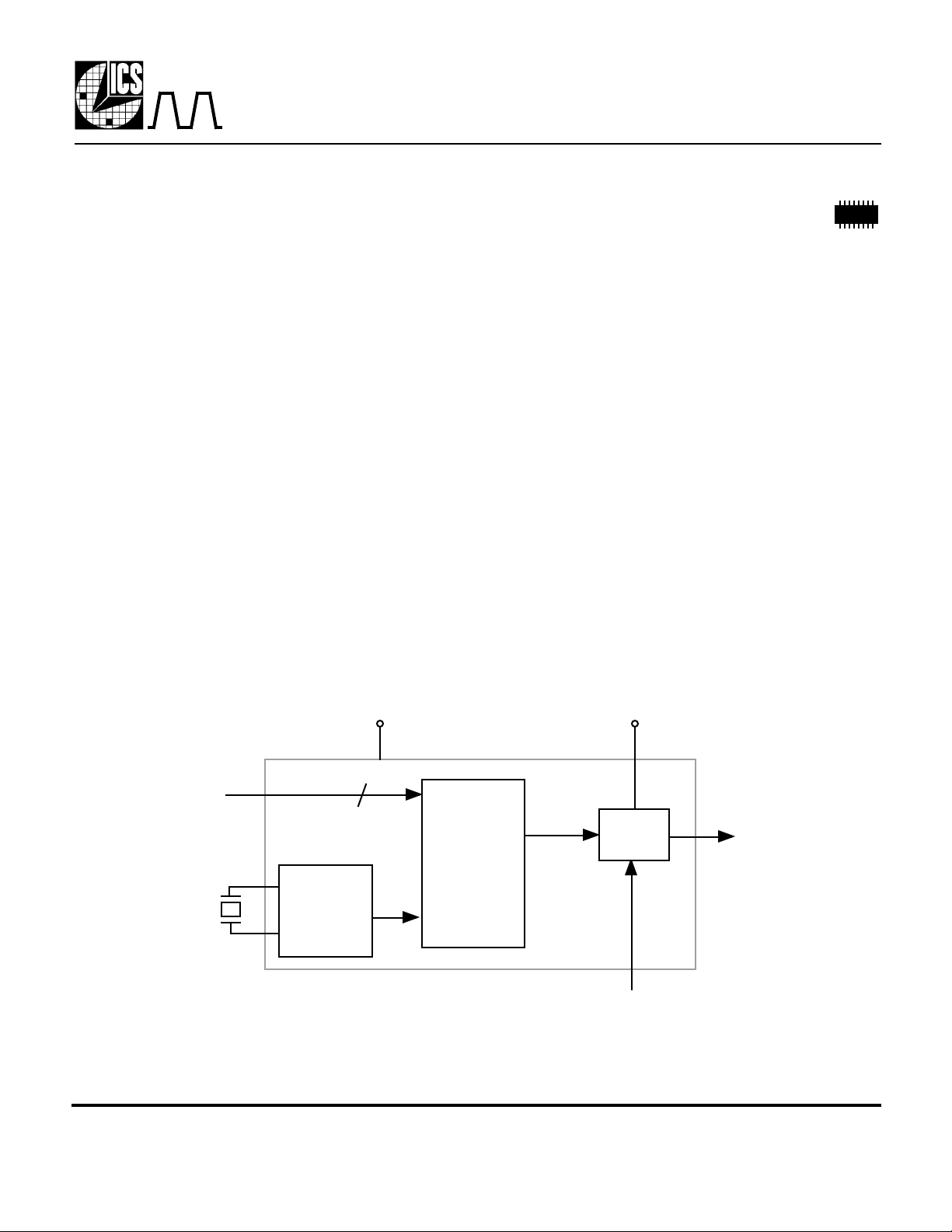
Block Diagram
S2:0
20 MHz
crystal
X1
X2
3
Crystal
Oscillator
VDD
PLL/Clock
Synthesis
Circuitry
VDDP
Output
Buffer
Output Enable
CLK
MDS 1711-01 B 1 Revision 120897 Printed 11/15/00
MicroClock Division of ICS•1271 Parkmoor Ave.•San Jose•CA•95126•(408)295-9800tel•(408)295-9818fax
Page 2
MK1711-01
Pin Assignment
MK1711-01
X1
VDD
VDD
VDDP
GND
GND
SEL3V
INVCLK
16 pin narrow (150 mil) SOIC
ICRO
16
1
15
2
14
3
13
4
12
5
11
6
10
7
8
9
C
LOCK
X2
OE
NC
CLK
NC
S0
S1
S2
200 MHz Selectable Clock Source
Output Clock Select Table (MHz)
Input S2 S1 S0 CLK1
20 0 0 0 200
20 0 0 1 182
20 0 1 0 167
20 0 1 1 154
20 1 0 0 143
20 1 0 1 133
20 1 1 0 125
20 1 1 1 118
Pin Descriptions
Number Name Type Description
1 X1 XI Crystal connection. Connect to a 20.00 MHz crystal.
2 VDD P VDD. Connect to +3.3V (Possibly 5V).
3 VDD P VDD. Connect to +3.3V (Possibly 5V).
4 VDDP P Connect to 3.3V only.
5 GND P Connect to ground.
6 GND P Connect to ground.
7 SEL3V I Select 3.3V only power supply. Connect to GND for VDD=5V. Internal pull-up.
8 INVCLK I Inverts output clock. Internal pull-up.
9 S2 I Clock Select 2. Selects output per table above. Internal pull-up.
10 S1 I Clock Select 1. Selects output per table above. Internal pull-up.
11 S0 I Clock Select 0. Selects output per table above. Internal pull-up.
12 NC - No Connect. Nothing is connected internally to this pin.
13 CLK O Clock output determined by status of S2, S1, S0. See table above.
14 NC - No Connect. Nothing is connected internally to this pin.
15 OE I Output Enable. Active high. Tri-states clock output when low. Internal pull-up.
16 X2 XO Crystal connection. Connect to a 20.00 MHz crystal.
Key: I = Input, O = output, P = power supply connection
MDS 1711-01 B 2 Revision 120897 Printed 11/15/00
MicroClock Division of ICS•1271 Parkmoor Ave.•San Jose•CA•95126•(408)295-9800tel•(408)295-9818fax
Page 3

MK1711-01
ABSOLUTE MAXIMUM RATINGS (note 1)
DC CHARACTERISTICS (VDD = 5.0V unless noted)
AC CHARACTERISTICS (VDD = 5.0V unless noted)
exposure to levels above the operating limits but below the Absolute Maximums may affect device reliability.
2. With VDD at 3.3V and CLK at 200MHz.
ICRO
C
LOCK
200 MHz Selectable Clock Source
Electrical Specifications
Parameter Conditions Minimum Typical Maximum Units
Supply voltage, VDD Referenced to GND 7 V
Inputs and Clock Outputs Referenced to GND -0.5 VDD+0.5 V
Ambient Operating Temperature 0 70 °C
Soldering Temperature Max of 10 seconds 260 °C
Storage temperature -65 150 °C
Operating Voltage, VDD 3.00 5.25 V
Input High Voltage, VIH, X1 pin only 3.5 2.5 V
Input Low Voltage, VIL, X1 pin only 2.5 1.5 V
Input High Voltage, VIH 2 V
Input Low Voltage, VIL 0.8 V
Output High Voltage, VOH IOH=-50mA 2.4 V
Output Low Voltage, VOL IOL=50mA 0.4 V
Output High Voltage, VOH, CMOS level IOH=-16mA VDD-0.4 V
Operating Supply Current, IDD No Load, note 2 8 mA
Short Circuit Current TBD mA
Input Capacitance S2, S1, S0, OE 7 pF
Frequency synthesis error All clocks 0 ppm
Input Crystal Frequency
Input Crystal Accuracy ±50 ppm
Output Clock Rise Time, 200 MHz 0.8 to 2.0V 0.6 ns
Output Clock Fall Time, 200MHz 2.0 to 0.8V 0.6 ns
Output Clock Duty Cycle At VDD/2 45 55 %
Maximum Absolute Jitter, short term 200 ±350 ps
Notes: 1. Stresses beyond those listed under Absolute Maximum Ratings could cause permanent damage to the device. Prolonged
20.00000
MHz
External Components
The MK1711-01 requires a minimum number of external components for proper operation. Decoupling
capacitors of 0.1µF should be connected between VDD and GND (pins 3 and 5), as close to the MK171101 as possible. A series termination resistor of 33Ω may be used for the clock output. The input crystal
must be connected as close to the chip as possible. The input crystal should be a parallel mode, 20 MHz
fundamental, with 20pF load capacitance.
MDS 1711-01 B 3 Revision 120897 Printed 11/15/00
MicroClock Division of ICS•1271 Parkmoor Ave.•San Jose•CA•95126•(408)295-9800tel•(408)295-9818fax
Page 4

MK1711-01
Inches
Millimeters
ICRO
C
LOCK
Package Outline and Package Dimensions
E H
h x 45°
D
Q
e
b
c
200 MHz Selectable Clock Source
16 pin SOIC narrow
Symbol Min Max Min Max
A 0.055 0.070 1.397 1.778
b 0.013 0.019 0.330 0.483
c 0.007 0.010 0.191 0.254
D 0.385 0.400 9.779 10.160
E 0.150 0.160 3.810 4.064
H 0.225 0.245 5.715 6.223
e
h 0.016 0.406
Q 0.004 0.01 0.102 0.254
A
Ordering Information
Part/Order Number Marking Shipping packaging Package Temperature
MK1711-01S MK1711-01S tubes 16 pin SOIC 0-70°C
MK1711-01STR MK1711-01S tape and reel 16 pin SOIC 0-70°C
While the information presented herein has been checked for both accuracy and reliability, MicroClock Incorporated assumes no responsibility for either its use or for the
infringement of any patents or other rights of third parties, which would result from its use. No other circuits, patents, or licenses are implied. This product is intended for use in
normal commercial applications. Any other applications such as those requiring extended temperature range, high reliability, or other extraordinary environmental requirements
are not recommended without additional processing by MicroClock. MicroClock reserves the right to change any circuitry or specifications without notice. MicroClock does not
authorize or warrant any MicroClock product for use in life support devices or critical medical instruments.
MDS 1711-01 B 4 Revision 120897 Printed 11/15/00
MicroClock Division of ICS•1271 Parkmoor Ave.•San Jose•CA•95126•(408)295-9800tel•(408)295-9818fax
 Loading...