

Page 1
MK1574
ICRO
C
LOCK
Description
The MK1574-01 is a Phase-Locked Loop (PLL)
based clock synthesizer, which accepts an 8 kHz
clock input as a reference, and generates many
popular communications frequencies. All outputs
are frequency locked together and to the input.
This allows for the generation of locked clocks to
the 8 kHz backplane clock, simplifying clock
generation and distribution in communications
systems.
MicroClock can customize this device for any
other different frequencies.
Frame Rate Communications PLL
Features
• Packaged in 16 pin narrow (150 mil) SOIC
• Exact multiplications stored in the device eliminate
the need for external dividers
• Accepts 8 kHz input clock
• Output clock rates include T1, E1, T2, E2
• 3.0V to 5.5V operation
• Available in commercial (0 to +70 C) or industrial
(-40 to +85 C) temperature ranges
• For jitter attenuation, use the MK2049
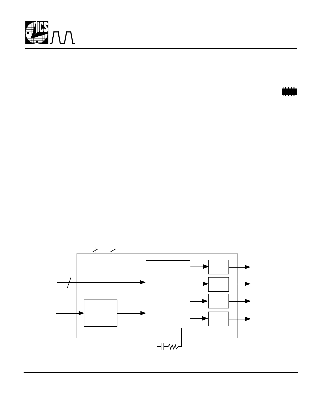
Block Diagram
VDD GND
2
4
FS0-3
8kHz
Input Clock
MDS 1574-01 D 1 Revision 011999 Printed 11/15/00
MicroClock Division of ICS • 525 Race Street • San Jose • CA • 95126•(408)295-9800tel•(408)295-9818fax
Input
Buffer
2
CAP1
PLL
Clock
Synthesis
and
Control
Circuitry
Output
Buffer
Output
Buffer
Output
Buffer
Output
Buffer
CAP2
CLK1
CLK2
CLK3
8kHz
(recovered)
Page 2
MK1574
ICRO
C
LOCK
Frame Rate Communications PLL
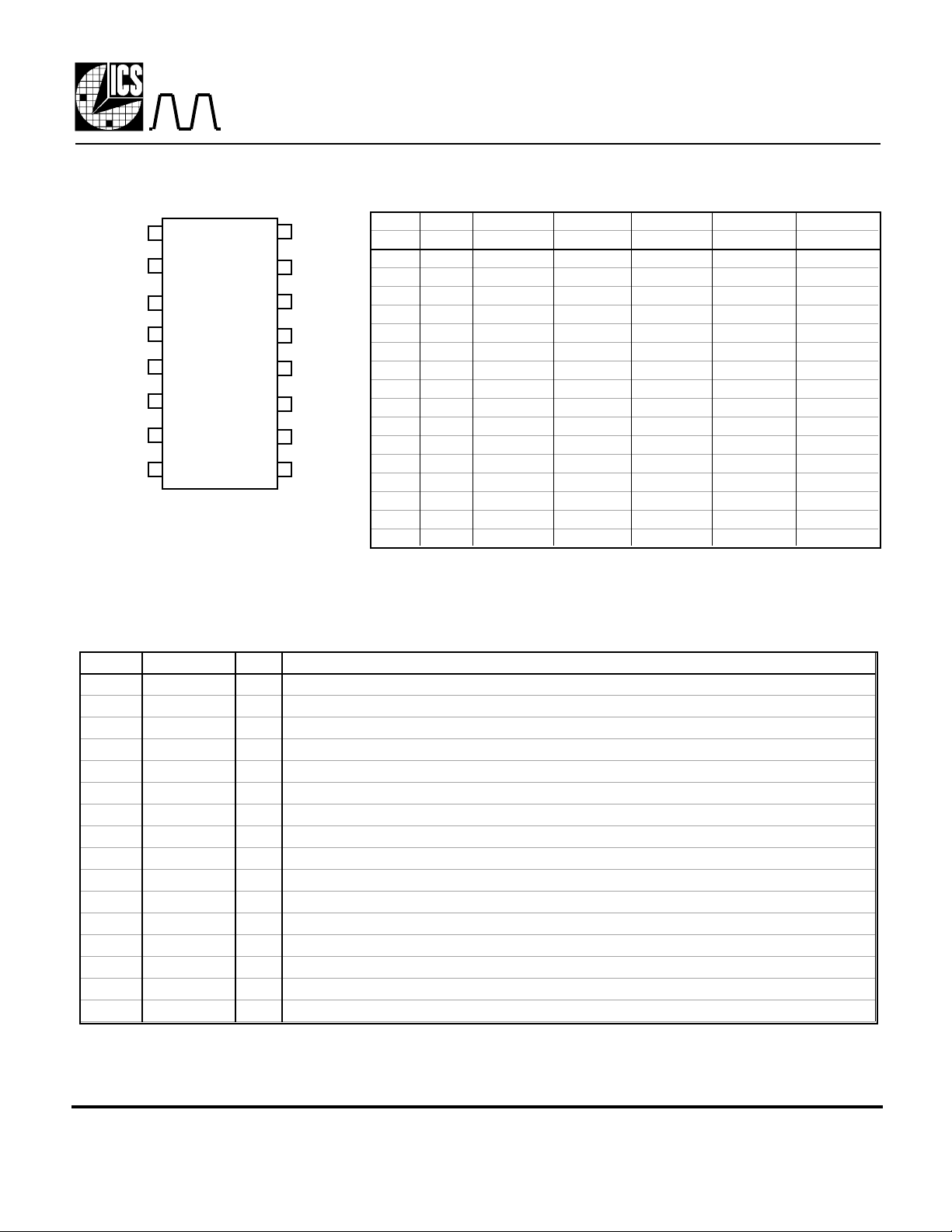
Pin Assignment Output Clocks Decoding Table MK1574-01 (MHz)
ICLK
VDD
VDD
CAP1
GND
CAP2
GND
1
2
3
4
5
16
15
14
13
12
6
7
10
8
16 pin (150 mil) SOIC
11
9FS0
FS3
N/C
FS2
FS1
CLK3
CLK2
CLK1
8KOUT
Decode Address ICLK Multiplier CLK 1 CLK 2 CLK 3
FS3:0 (Hex) pin 1 On-chip pin 10 pin 11 pin 12
0 Reserved Reserved Reserved Reserved Reserved
0000
1 Reserved Reserved Reserved Reserved Reserved
0001
2 Reserved Reserved Reserved Reserved Reserved
0010
3 Reserved Reserved Reserved Reserved Reserved
0011
4 8.00kHz 2940 23.52 11.76 5.88
0100
5 8.00kHz 1960 15.68 7.84 3.92
0101
6 8.00kHz 2760 22.08 11.04 5.52
0110
7 8.00kHz 2640 21.12 10.56 5.28
0111
8 8.00kHz 1920 15.36 7.68 3.84
1000
9 8.00kHz 6480 51.84 25.92 12.96
1001
A 8.00kHz 2112 16.896 8.448 4.224
1010
B 8.00kHz 1578 12.624 6.312 3.156
1011
C 8.00kHz 8192 65.536 32.768 16.384
1100
D 8.00kHz 6176 49.408 24.704 12.352
1101
E 8.00kHz 1024 8.192 4.096 2.048
1110
F 8.00kHz 772 6.176 3.088 1.544
1111
• 0 = connect directly to ground, 1 = connect directly to VDD.
Pin Descriptions
Number Name Type Description
1 ICLK I Input clock. Connect to an 8kHz clock input.
2 VDD P Connect to +3.3V or +5V.
3 VDD P Connect to +3.3V or +5V. Must be same voltage as pin 2.
4 CAP1 I Connect a ceramic capacitor and a resistor in series between this pin and CAP2. Refer to page 4.
5 GND P Connect to ground.
6 CAP2 I Connect a ceramic capacitor and a resistor in series between this pin and CAP1. Refer to page 4.
7 GND P Connect to ground.
8 FS0 I Frequency Select 0. Determines CLK outputs per table above.
9 8KOUT O Recovered 8kHz output clock. Can be lower jitter, better duty cycle than input clock.
10 CLK1 O Clock 1 determined by status of FS3:0 per table above.
11 CLK2 O Clock 2 determined by status of FS3:0 per table above.
12 CLK3 O Clock 3 determined by status of FS3:0 per table above.
13 FS1 I Frequency Select 1. Determines CLK outputs per table above.
14 FS2 I Frequency Select 2. Determines CLK outputs per table above.
15 N/C - No Connect. Nothing is connected to this pin.
16 FS3 I Frequency Select 3. Determines CLK outputs per table above.
Type: I = Input, O = output, P = power supply connection
MDS 1574-01 D 2 Revision 011999 Printed 11/15/00
MicroClock Division of ICS • 525 Race Street • San Jose • CA • 95126•(408)295-9800tel•(408)295-9818fax
Page 3

MK1574
ABSOLUTE MAXIMUM RATINGS (Note 1)
DC CHARACTERISTICS (VDD = 5V unless noted)
AC CHARACTERISTICS (VDD = 5V unless noted)
ICRO
C
LOCK
Frame Rate Communications PLL
External Components/Crystal Selection
The MK1574 requires a minimum number of external components for proper operation. An RC network
(see Capacitor Selection on following page) should be connected between CAP1 and CAP2 as close to the
chip as possible. A high quality ceramic capacitor is recommended. A decoupling capacitor of 0.1µF must
be connected between VDD and GND pins (pins 2 and 3, 5 and 7) close to the chip, and 33Ω terminating
resistors can be used on clock outputs with traces longer than 1 inch.
Electrical Specifications
Parameter Conditions Minimum Typical Maximum Units
Supply Voltage, VDD Referenced to GND 7 V
Inputs and Clock Outputs -0.5 VDD+0.5 V
Ambient Operating Temperature 0 70 °C
Soldering Temperature Max of 10 seconds 250 °C
Storage Temperature -65 150 °C
Operating Voltage, VDD 3 5.5 V
Input High Voltage, VIH 2 V
Input Low Voltage, VIL 0.8 V
Output High Voltage IOH=-4mA VDD-0.4 V
Output High Voltage IOH=-25mA 2.4 V
Output Low Voltage IOL=25mA 0.4 V
Operating Supply Current, IDD No Load, VDD=5.0V 15 mA
Short Circuit Current Each output ±100 mA
Input Capacitance 7 pF
Input Frequency 8.0000 kHz
Output Clock Rise Time 0.8 to 2.0V 1.5 ns
Output Clock Fall Time 2.0 to 0.8V 1.5 ns
Output Clock Duty Cycle, High Time At VDD/2 40 49 to 51 60 %
Absolute Clock Period Jitter 1 ns
Actual mean frequency error versus target, note 2 Any clock selection 0 0 ppm
Notes:
1. Stresses beyond those listed under Absolute Maximum Ratings could cause permanent damage to the device. Prolonged exposure
to levels above the operating limits but below the Absolute Maximums may affect device reliability.
2. All multipliers as shown in the table on page two are exact, and are stored in ROM on the chip.
MDS 1574-01 D 3 Revision 011999 Printed 11/15/00
MicroClock Division of ICS • 525 Race Street • San Jose • CA • 95126•(408)295-9800tel•(408)295-9818fax
Page 4

MK1574
ICRO
C
LOCK
Frame Rate Communications PLL
Loop Bandwidth and Loop Filter Component Selection
The series-connected capacitor and resistor between CAP1 and CAP2 (pins 4 and 6) determine the dynamic
characteristics of the phase-locked loop. The capacitor must have very low leakage, therefore a high quality
ceramic capacitor is recommended. DO NOT use any type of polarized or electrolytic capacitor. The series
connected capacitor and resistor between CAP1 and CAP2 (pins 4 and 6) determine the dynamic
characteristics of the phase-locked loop. The capacitor must have very low leakage, therefore a high quality
ceramic capacitor is recommended. DO NOT use any type of polarized or electrolytic capacitor. Ceramic
capacitors should have C0G or NP0 dielectric. Avoid high-K dielectrics like Z5U and X7R; these and other
ceramics which have piezoelectric properties allow mechanical vibration in the system to increase the output
jitter because the mechanical energy is converted directly to voltage noise on the VCO input.
The values of the RC network determine the bandwidth of the PLL. The values of the loop filter components
are calculated using the constants K1 and K2 from the table on page 5. The loop bandwidth is set by the
capacitor C and the constant K1 using the formula
K1
C
The loop damping is set by the resistor R, the capacitor C, and the constant K2 using the formula
Equation 1BW (Hz) =
R =
For example, to design the loop filter when generating 8.192 MHz from 8 kHz:
1. From the table on page 2, the address is E. The table on page 5 shows constants K1=0.0516 and K2=6.2.
2. A good value for the loop bandwidth is 1/20 the input frequency; where 8 kHz/20 = 400 Hz. Using
Equation 1,
400 =
Therefore,
3. A good value for the damping factor ζ is 0.707. From Equation 2,
C =
R =
ζ • K2
C
0.0516
C
0.0516
( )
400
0.707 • 6.2
16E-9
Equation 2; ζ (zeta) is the damping factor
2
= 16.6 nF (16 nF nearest standard value)
= 34.7 kΩ (36 kΩ nearest standard value)
MDS 1574-01 D 4 Revision 011999 Printed 11/15/00
MicroClock Division of ICS • 525 Race Street • San Jose • CA • 95126•(408)295-9800tel•(408)295-9818fax
Page 5

MK1574
ICRO
C
LOCK
Frame Rate Communications PLL
Loop Filter Constants
This table shows the constants K1 and K2 that are used with the equations on page 4 to calculate the
external loop filter components.
Loop Filter Constants for MK1574-01
Decode Address Loop Filter Constants
FS3:0 (Hex) K1 K2
0 Reserved Reserved
0000
1 Reserved Reserved
0001
2 Reserved Reserved
0010
3 Reserved Reserved
0011
4 0.0430 7.4
0100
5 0.0527 6.0
0101
6 0.0444 7.2
0110
7 0.0454 7.0
0111
8 0.0533 6.0
1000
9 0.0410 7.8
1001
A 0.0508 6.3
1010
B 0.0587 5.4
1011
C 0.0365 8.7
1100
D 0.0420 7.6
1101
E 0.0516 6.2
1110
F 0.0594 5.4
1111
PC Board Layout
A proper board layout is critical to the successful
use of the MK1574. In particular, the CAP1 and
CAP2 pins are very sensitive to noise and leakage
(CAP1 at pin 4 is the most sensitive). Traces
must be as short as possible and the capacitor
and resistor must be mounted next to the device
as shown to the right. The capacitor connected
between pins 3 and 5 is the power supply
decoupling capacitor.
cap
V
cap
G
resist.
1
16
2
15
3
14
4
13
12
5
11
6
10
7
8
9
=connect to VDD
V
=connect to GND
G
The high frequency output clocks on may
benefit from a series 33Ω resistor connected
close to the pin (not shown).
Clock Multipliers/Accuracies
In the table on page 2 are the actual multipliers stored in the MK1574 ROM, which yield the exact values
shown for the output clocks.
MDS 1574-01 D 5 Revision 011999 Printed 11/15/00
MicroClock Division of ICS • 525 Race Street • San Jose • CA • 95126•(408)295-9800tel•(408)295-9818fax
Page 6

MK1574
Inches
Millimeters
ICRO
C
LOCK
Package Outline and Package Dimensions
E H
h x 45°
D
Q
e
b
c
Frame Rate Communications PLL
16 pin SOIC narrow
Symbol Min Max Min Max
A 0.055 0.070 1.397 1.778
b 0.013 0.019 0.330 0.483
c 0.007 0.010 0.191 0.254
D 0.385 0.400 9.779 10.160
E 0.150 0.160 3.810 4.064
H 0.225 0.245 5.715 6.223
e
h 0.016 0.406
Q 0.004 0.01 0.102 0.254
A
Ordering Information
Part/Order Number Marking Package Temperature
MK1574-01S MK1574-01S 16 pin narrow SOIC 0 to 70°C
MK1574-01STR MK1574-01S Add Tape & Reel 0 to 70°C
MK1574-01SI MK1574-01S 16 pin narrow SOIC -40 to +85°C
MK1574-01SITR MK1574-01S Add Tape & Reel -40 to +85°C
While the information presented herein has been checked for both accuracy and reliability, Integrated Circuit Systems, Incorporated (ICS) assumes no responsibility for either its
use or for the infringement of any patents or other rights of third parties, which would result from its use. No other circuits, patents, or licenses are implied. This product is
intended for use in normal commercial applications. Any other applications such as those requiring extended temperature range, high reliability, or other extraordinary
environmental requirements are not recommended without additional processing by ICS. ICS reserves the right to change any circuitry or specifications without notice. ICS does
not authorize or warrant any ICS product for use in life support devices or critical medical instruments.
CHANGE HISTORY
Version Date first published Comments
A 1/24/97 Original
B 2/3/98 Added I grade, revised filter equations, updated address.
C 2/23/98 Added Absolute Jitter value.
D 1/19/99 Added additional capacitor requirements.
MDS 1574-01 D 6 Revision 011999 Printed 11/15/00
MicroClock Division of ICS • 525 Race Street • San Jose • CA • 95126•(408)295-9800tel•(408)295-9818fax
 Loading...