

Page 1
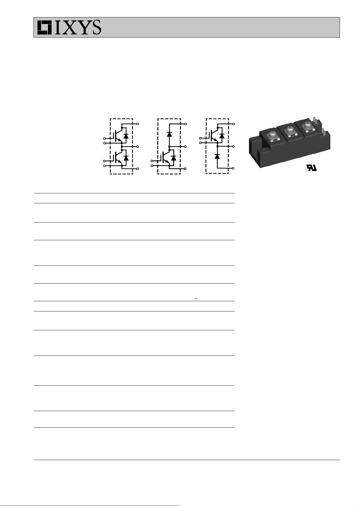
MII 145-12 A3 MID 145-12 A3
MDI 145-12 A3
IGBT Modules
Short Circuit SOA Capability
Square RBSOA
MII
1
7
6
4
5
3
2
Symbol Conditions Maximum Ratings
V
CES
V
CGR
V
GES
V
GEM
I
C25
I
C80
I
CM
t
SC
TJ= 25°C to 150°C 1200 V
TJ= 25°C to 150°C; RGE = 20 kW 1200 V
Continuous ±20 V
Transient ±30 V
TC= 25°C 160 A
TC= 80°C 110 A
TC= 80°C, tp = 1 ms 220 A
VGE = ±15 V, VCE = V
, TJ = 125°C10ms
CES
(SCSOA) RG= 6.8 W, non repetitive
RBSOA V
= ±15 V, TJ = 125°C, RG = 6.8 W ICM = 200 A
GE
Clamped inductive load, L = 100 mHV
P
tot
T
J
T
stg
V
ISOL
M
d
TC= 25°C 700 W
50/60 Hz, RMS t = 1 min 4000 V~
I
£ 1 mA t = 1 s 4800 V~
ISOL
Insulating material: Al2O
3
Mounting torque (module) 2.25-2.75 Nm
(teminals) 2.5-3.7 Nm
d
S
d
A
Creepage distance on surface 12.7 mm
Strike distance through air 9.6 mm
a Max. allowable acceleration 50 m/s
Weight Typical 130 g
MID
1
3
4
5
2
< V
CEK
MDI
7
6
CES
150 °C
-40 ... +150 °C
20-25 lb.in.
22-33 lb.in.
4.6 oz.
I
C25
V
CES
V
CE(sat) typ.
1
3
2
= 160 A
= 1200 V
= 2.2 V
3
1
2
Features
●
NPT IGBT technology
●
low saturation voltage
●
low switching losses
●
switching frequency up to 30 kHz
●
square RBSOA, no latch up
●
high short circuit capability
●
positive temperature coefficient for
easy parallelling
●
MOS input, voltage controlled
●
ultra fast free wheeling diodes
●
package with DCB ceramic base plate
●
isolation voltage 4800 V
●
UL registered E72873
Advantages
●
space and weight savings
●
reduced protection circuits
Typical Applications
●
AC and DC motor control
●
AC servo and robot drives
●
power supplies
●
welding inverters
2
4
5
E 72873
6
7
Data according to a single IGBT/FRED unless otherwise stated.
© 2000 IXYS All rights reserved
030
1 - 4
Page 2
MII 145-12 A3 MID 145-12 A3
MDI 145-12 A3
Symbol Conditions Characteristic Values
(TJ = 25°C, unless otherwise specified)
min. typ. max.
V
(BR)CES
V
GE(th)
I
CES
VGE = 0 V 1200 V
IC = 4 mA, VCE = V
VCE= V
CES
GE
TJ = 25°C6mA
4.5 6.5 V
TJ = 125°C9mA
I
GES
V
C
C
C
t
d(on)
t
r
t
d(off)
t
f
E
E
R
R
CE(sat)
ies
oes
res
on
off
thJC
thJS
VCE= 0 V, VGE = ±20 V ±400 nA
IC = 100 A, VGE = 15 V 2.2 2.7 V
6.5 nF
VCE = 25 V, VGE = 0 V, f = 1 MHz 1 nF
0.5 nF
100 ns
Inductive load, T
= 100 A, VGE = ±15 V
I
C
= 125°C
J
VCE = 600 V, RG = 6.8 W
60 ns
600 ns
90 ns
16 mJ
15 mJ
0.18 K/W
with heatsink compound 0.36 K/W
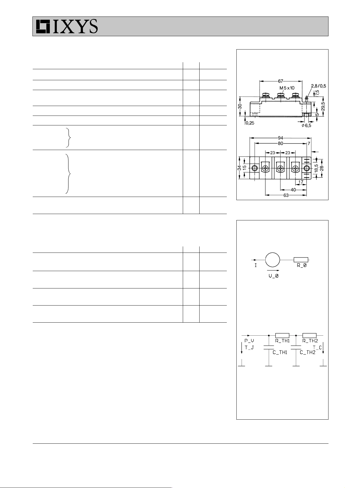
Dimensions in mm (1 mm = 0.0394")
Reverse Diode (FRED) Characteristic Values
= 25°C, unless otherwise specified)
(T
J
min. typ. max.
V
F
IF = 100 A, VGE = 0 V, 2.4 2.6 V
IF = 100 A, VGE = 0 V, TJ = 125°C 1.9 2.0 V
I
F
TC = 25°C 150 A
TC = 80°C95A
I
RM
t
rr
R
thJC
R
thJS
IF = 100 A, VGE = 0 V, -diF/dt = 600 A/ms62A
TJ = 125°C, VR = 600 V 200 ns
0.45 K/W
with heatsink compound 0.9 K/W
Equivalent Circuits for Simulation
Conduction
IGBT (typ. at VGE = 15 V; TJ = 125°C)
V0 = 1.3 V; R0 = 12.0 mW
Free Wheeling Diode (typ. at TJ = 125°C)
Thermal Response
IGBT (typ.)
V0 = 1.3 V; R0 = 6.5 mW
C
= 0.25 J/K; R
th1
C
= 0.58 J/K; R
th2
= 0.175 K/W
th1
= 0.004 K/W
th2
© 2000 IXYS All rights reserved
Free Wheeling Diode (typ.)
C
= 0.14 J/K; R
th1
C
= 0.26 J/K; R
th2
= 0.443 K/W
th1
= 0.009 K/W
th2
2 - 4
Page 3

MII 145-12 A3 MID 145-12 A3
MDI 145-12 A3
250
TJ = 25°C
A
200
I
C
150
100
50
0
0.0 0.5 1.0 1.5 2.0 2.5 3.0
VGE=17V
15V
13V
11V
9V
V
V
CE
250
T
= 125°C
J
A
200
I
C
150
100
50
0
0.00.51.01.52.02.53.03.5
Fig. 1 Typ. output characteristics Fig. 2 Typ. output characteristics
250
VCE = 20V
A
= 25°C
T
J
200
I
C
150
100
300
A
250
I
F
200
150
100
= 125°C
T
J
VGE=17V
15V
13V
11V
9V
V
V
CE
TJ = 25°C
50
0
567891011
V
GE
V
50
0
01234
Fig. 3 Typ. transfer characteristics Fig. 4 Typ. forward characteristics of
free wheeling diode
20
VCE = 600V
V
= 100A
I
C
15
V
GE
10
5
0
0 100 200 300 400 500
Q
nC
G
120
A
I
RM
t
rr
80
40
I
RM
0
0 200 400 600 800 1000
Fig. 5 Typ. turn on gate charge Fig. 6 Typ. turn off characteristics of
free wheeling diode
V
F
TJ = 125°C
V
= 600V
R
I
= 100A
F
-di/dt
A/ms
V
145-12
300
ns
200
100
0
t
rr
© 2000 IXYS All rights reserved
3 - 4
Page 4

MII 145-12 A3 MID 145-12 A3
MDI 145-12 A3
40
mJ
30
E
on
20
10
0
0 50 100 150 200
Fig. 7 Typ. turn on energy and switching Fig. 8 Typ. turn off energy and switching
times versus collector current times versus collector current
50
V
= 600V
CE
mJ
40
E
on
30
= ±15V
V
GE
= 100A
I
C
T
= 125°C
J
t
d(on)
E
on
I
C
t
r
VCE = 600V
= ±15V
V
GE
R
= 6.8
W
G
TJ = 125°C
E
t
d(on)
t
r
120
ns
90
t
60
30
0
A
300
on
ns
240
t
180
40
mJ
30
E
off
20
10
0
0 50 100 150 200
25
V
= 600V
CE
mJ
20
E
off
= ±15V
V
GE
I
= 100A
C
= 125°C
T
J
15
I
C
VCE = 600V
= ±15V
V
GE
R
= 6.8
G
TJ = 125°C
t
E
t
d(off)
f
t
E
off
W
A
d(off)
off
800
ns
600
t
400
200
0
1500
ns
1200
t
900
20
10
0
0 8 16 24 32 40 48 56
Fig. 9 Typ. turn on energy and switching Fig.10 Typ. turn off energy and switching
times versus gate resistor times versus gate resistor
240
A
200
I
CM
160
120
RG = 6.8
= 125°C
T
J
< V
V
CEK
W
CES
80
40
0
0 200 400 600 800 1000 1200
Fig. 11 Reverse biased safe operating area Fig. 12 Typ. transient thermal impedance
RBSOA
120
60
0
W
R
G
10
5
0
0 8 16 24 32 40 48 56
R
G
600
300
t
f
0
W
1
K/W
0.1
Z
thJC
0.01
diode
IGBT
0.001
0.0001
0.00001
V
V
CE
0.00001 0.0001 0.001 0.01 0.1 1
single pulse
145-12
s
t
© 2000 IXYS All rights reserved
4 - 4
 Loading...