

Page 1
MIC7111 Micrel
MIC7111
1.8V IttyBitty™ Rail-to-Rail Input/Output Op Amp
Preliminary Information
General Description
The MIC7111 is a micropower operational amplifier featuring
rail-to-rail input and output performance in Micrel’s IttyBitty
SOT-23-5 package. The MIC7111 is ideal for systems where
small size is a critical consideration.
The MIC7111 is designed to operate from 1.8V to 11V power
supplies.
The MIC7111 benefits small battery operated portable electronic devices where small size and the ability to place the
amplifier close to the signal source are primary design
concerns.
For other package options, please contact the factory.
™
Features
• Small footprint SOT-23-5 package
• Guaranteed performance at 1.8V, 2.7V, 5V, and 10V
•15µA typical supply current at 1.8V
• 25kHz gain-bandwidth at 5V
• Output swing to within 1mV of rails
with 1.8V supply and 100kΩ load
• Suitable for driving capacitive loads
Applications
• Wireless and cellular communications
• GaAs RF amplifier bias amplifier
• Current sensing for battery chargers
• Reference voltage buffer
• Transducer linearization and interface
• Portable computing
Ordering Information
Part Number Junction Temp. Range Package
MIC7111BM5 –40°C to +85°C SOT-23-5
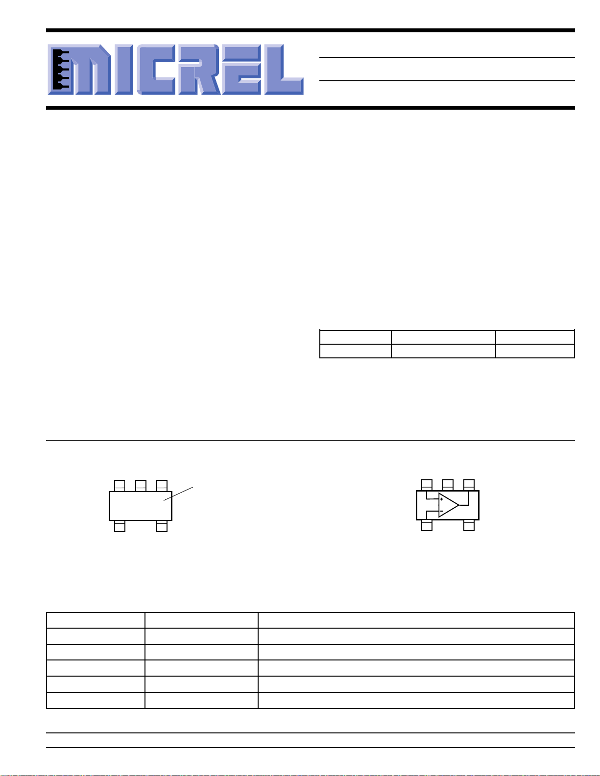
Pin Configuration
IN+
2
OUTV+
13
Part
Identification
Functional Configuration
IN+
OUTV+
2
13
A13
45
IN–
V–
45
IN–
V–
SOT-23-5 (M5)
Pin Description
Pin Number Pin Name Pin Function
1 OUT Amplifier Output
2 V+ Positive Supply
3 IN+ Noninverting Input
4 IN– Inverting Input
5 V– Negative Suppy
IttyBitty is a trademark of Micrel, Inc.
Micrel, Inc. • 1849 Fortune Drive • San Jose, CA 95131 • USA • tel + 1 (408) 944-0800 • fax + 1 (408) 944-0970 • http://www.micrel.com
June 1998 1 MIC7111
Page 2
MIC7111 Micrel
Absolute Maximum Ratings (Note 1)
Supply Voltage (VV+ – VV–)...........................................12V
Differential Input Voltage (V
I/O Pin Voltage (VIN, V
OUT
.............................................V
Junction Temperature (TJ) ...................................... +150°C
– V
IN+
), Note 2
) ...........±(VV+ – VV–)
IN–
+ 0.3V to V
V+
V–
– 0.3V
Operating Ratings (Note 1)
Supply Voltage (VV+ – VV–).............................. 1.8V to 11V
Junction Temperature (TJ) ......................... –40°C to +85°C
Max. Junction Temperature (T
Package Thermal Resistance (θJA), Note 4..........325°C/W
Max. Power Dissipation............................................ Note 3
), Note 3 ...........+85°C
J(max)
Storage Temperature ...............................–65°C to +150°C
Lead Temperature (soldering, 10 sec.) .....................260°C
ESD, Note 5.................................................................. 2kV
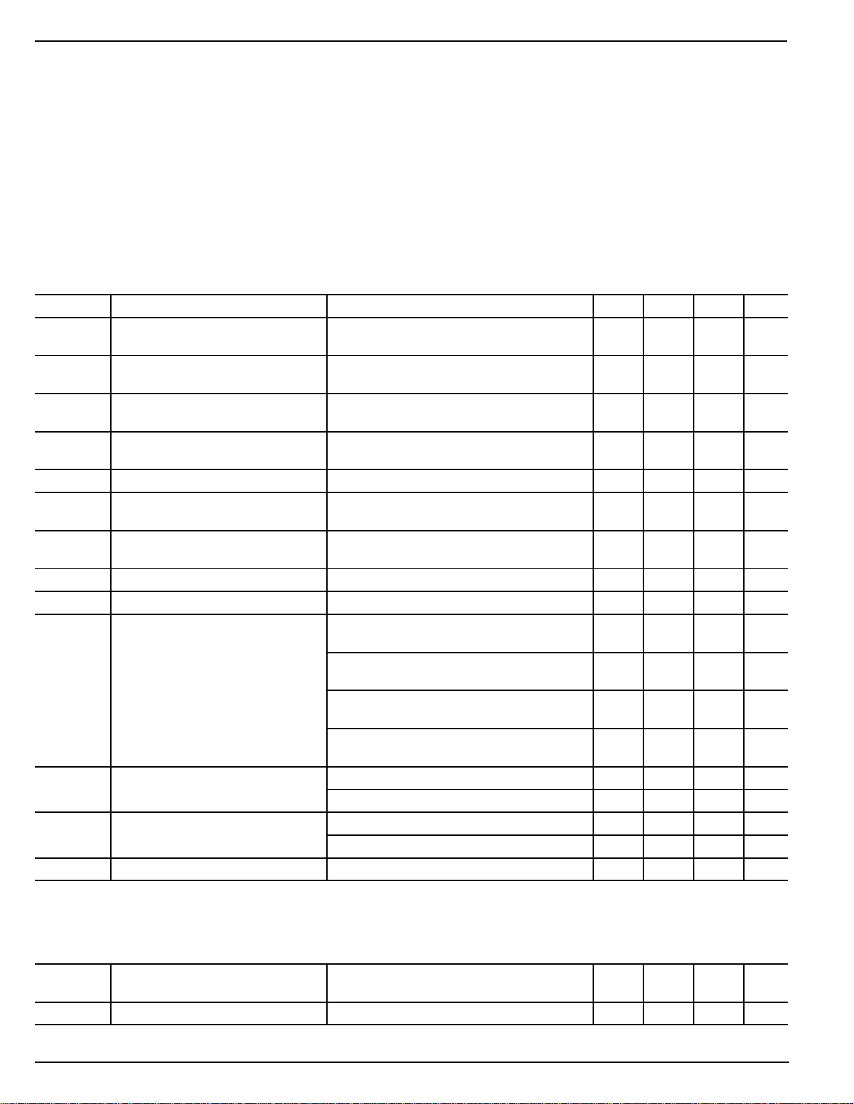
DC Electrical Characteristics (1.8V)
VV+ = +1.8V, VV– = 0V, VCM = V
Symbol Parameter Condition Min Typ Max Units
V
OS
TCV
OS
Input Offset Voltage 0.9 7 mV
Input Offset Voltage 2.0 µV/°C
Temperature Drift
I
B
I
OS
R
IN
Input Bias Current 110pA
Input Offset Current 0.01 0.5 pA
Input Resistance >10 TΩ
+PSRR Positive Power Supply 1.8V ≤ V
Rejection Ratio VCM = V
–PSRR Negative Power Supply –1.8V ≤ V
Rejection Ratio VCM = V
CMRR Common-Mode Rejection Ratio VCM = –0.2V to +2.0V 50 70 dB
C
V
I
IN
OUT
SC
Common Mode Input Capacitance 3 pF
Output Voltage Swing output high, RL = 100k, 0.14 1 mV
Output Short Circuit Current sourcing, V
Note 6
A
I
VOL
s
Voltage Gain sourcing 400 V/mV
Supply Current VV+ = 1.8V, V
= VV+/2; RL = 1M; TJ = 25°C, bold values indicate –40°C ≤ TJ ≤ +85°C; unless noted
OUT
≤ 5V, VV– = 0V, 60 85 dB
V+
= 0.9V
OUT
≤ –5V, VV+ = 0V, 60 85 dB
V–
= –0.9V
OUT
specified as VV+ – V
output low, R
output high, R
specified as VV+ – V
output low, R
OUT
sinking, V
OUT
OUT
= 100k 0.14 1 mV
L
= 2k, 6.8 23 mV
L
OUT
= 2k 6.8 23 mV
L
= 0V 15 25 mA
= 1.8V 15 25 mA
sinking 400 V/mV
= VV+/2 15 35 µA
OUT
9 mV
500 pA
75 pA
1 mV
1 mV
34 mV
34 mV
AC Electrical Characteristics (1.8V)
V+ = +1.8V, V– = 0V, VCM = V
SR Slew Rate voltage follower, 1V step, R
GBW Gain Bandwidth Product 25 kHz
MIC7111 2 June 1998
= VV+/2; RL = 1M; TJ = 25°C, bold values indicate –40°C ≤ TJ ≤ +85°C; unless noted
OUT
= 100k@0.9V 0.015 V/µs
V
OUT
= 1V
P–P
L
Page 3
MIC7111 Micrel
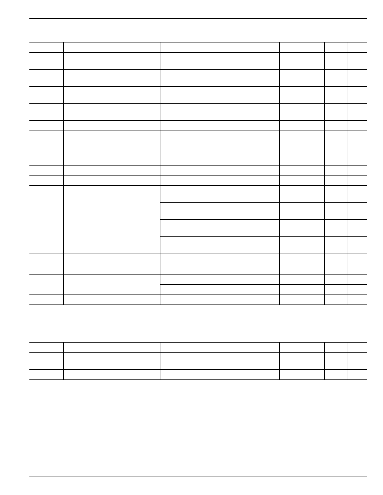
DC Electrical Characteristics (2.7V)
VV+ = +2.7V, VV– = 0V, VCM = V
Symbol Parameter Condition Min Typ Max Units
V
OS
TCV
OS
Input Offset Voltage 0.9 7 mV
Input Offset Voltage 2.0 µV/°C
Temperature Drift
I
B
I
OS
R
IN
Input Bias Current 110pA
Input Offset Current 0.01 0.5 pA
Input Resistance >10 TΩ
+PSRR Positive Power Supply 2.7V ≤ V
Rejection Ratio VCM = V
–PSRR Negative Power Supply –2.7V ≤ V
Rejection Ratio VCM = V
CMRR Common-Mode Rejection Ratio VCM = –0.2V to +2.9V 52 75 dB
C
V
I
IN
OUT
SC
Common Mode Input Capacitance 3 pF
Output Voltage Swing output high, RL = 100k, 0.2 1 mV
Output Short Circuit Current sourcing, V
Note 6
A
I
VOL
s
Voltage Gain sourcing 400 V/mV
Supply Current VV+ = 2.7V, V
= VV+/2; RL = 1M; TJ = 25°C, bold values indicate –40°C ≤ TJ ≤ +85°C; unless noted
OUT
≤ 5V, VV– = 0V, 60 90 dB
V+
= 1.35V
OUT
≤ –5V, VV+ = 0V, 60 90 dB
V–
= –1.35V
OUT
specified as VV+ – V
output low, R
output high, R
specified as VV+ – V
output low, R
OUT
sinking, V
OUT
OUT
= 100k 0.2 1 mV
L
= 2k, 10 33 mV
L
OUT
= 2k 10 33 mV
L
= 0V 30 50 mA
= 2.7V 30 50 mA
sinking 400 V/mV
= VV+/2 17 42 µA
OUT
9 mV
500 pA
75 pA
1 mV
1 mV
50 mV
50 mV
AC Electrical Characteristics (2.7V)
V+ = +2.7V, V– = 0V, VCM = V
Symbol Parameter Condition Min Typ Max Units
SR Slew Rate voltage follower, 1V step, R
GBW Gain Bandwidth Product 25 kHz
June 1998 3 MIC7111
= VV+/2; RL = 1M; TJ = 25°C, bold values indicate –40°C ≤ TJ ≤ +85°C; unless noted
OUT
= 100k@1.35V 0.015 V/µs
V
OUT
= 1V
P–P
L
Page 4

MIC7111 Micrel
DC Electrical Characteristics (5V)
VV+ = +5.0V, VV– = 0V, VCM = V
Symbol Parameter Condition Min Typ Max Units
V
OS
TCV
OS
Input Offset Voltage 0.9 7 mV
Input Offset Voltage 2.0 µV/°C
Temperature Drift
I
B
I
OS
R
IN
Input Bias Current 110pA
Input Offset Current 0.01 0.5 pA
Input Resistance >10 TΩ
+PSRR Positive Power Supply 5V ≤ V
Rejection Ratio VCM = V
–PSRR Negative Power Supply –5V ≤ V
Rejection Ratio VCM = V
CMRR Common-Mode Rejection Ratio VCM = –0.2V to +5.2V 57 80 dB
C
V
I
IN
OUT
SC
Common Mode Input Capacitance 3 pF
Output Voltage Swing output high, RL = 100k, 0.3 1.5 mV
Output Short Circuit Current sourcing, V
Note 6
A
I
VOL
S
Voltage Gain sourcing 500 V/mV
Supply Current VV+ = 5V, V
= VV+/2; RL = 1M; TJ = 25°C, bold values indicate –40°C ≤ TJ ≤ +85°C; unless noted
OUT
≤ 10V, VV– = 0V, 65 95 dB
V+
= 2.5V
OUT
≤ –10V, VV+ = 0V, 65 95 dB
V–
= –2.5V
OUT
specified as VV+ – V
output low, R
output high, R
specified as VV+ – V
output low, R
OUT
sinking, V
OUT
OUT
= 100k 0.3 1.5 mV
L
= 2k, 15 50 mV
L
OUT
= 2k 15 50 mV
L
= 0V 80 100 mA
= 5V 80 100 mA
sinking 500 V/mV
= VV+/2 20 50 µA
OUT
9 mV
500 pA
75 pA
1.5 mV
1.5 mV
75 mV
75 mV
AC Electrical Characteristics (5V)
V+ = +5V, V– = 0V, VCM = V
Symbol Parameter Condition Min Typ Max Units
SR Slew Rate voltage follower, 1V step, R
GBW Gain Bandwidth Product 25 kHz
= VV+/2; RL = 1M; TJ = 25°C, bold values indicate –40°C ≤ TJ ≤ +85°C; unless noted
OUT
= 100k@1.5V 0.02 V/µs
V
OUT
= 1V
P–P
L
DC Electrical Characteristics (10V)
VV+ = +10V, VV– = 0V, VCM = V
Symbol Parameter Condition Min Typ Max Units
V
OS
TCV
OS
Input Offset Voltage 0.9 7 mV
Input Offset Voltage 2.0 µV/°C
Temperature Drift
MIC7111 4 June 1998
= VV+/2; RL = 1M; TJ = 25°C, bold values indicate –40°C ≤ TJ ≤ +85°C; unless noted
OUT
9 mV
Page 5

MIC7111 Micrel
Symbol Parameter Condition Min Typ Max Units
I
B
I
OS
R
IN
+PSRR Positive Power Supply 5V ≤ V
–PSRR Negative Power Supply –5V ≤ V
CMRR Common-Mode Rejection Ratio VCM = –0.2V to +10.2V 60 85 dB
C
IN
V
OUT
I
SC
A
VOL
I
S
Input Bias Current 110pA
500 pA
Input Offset Current 0.01 0.5 pA
75 pA
Input Resistance >10 TΩ
≤ 10V, VV– = 0V, 65 95 dB
Rejection Ratio VCM = V
Rejection Ratio VCM = V
V+
= 2.5V
OUT
≤ –10V, VV+ = 0V, 65 95 dB
V–
= –2.5V
OUT
Common Mode Input Capacitance 3 pF
Output Voltage Swing output high, RL = 100k, 0.45 2.5 mV
specified as VV+ – V
output low, R
= 100k 0.45 2.5 mV
L
OUT
2.5 mV
2.5 mV
output high, R
specified as VV+ – V
output low, R
= 2k, 24 80 mV
L
OUT
= 2k 24 80 mV
L
120 mV
120 mV
Output Short Circuit Current sourcing, V
Note 6
sinking, V
= 0V 100 200 mA
OUT
= 10V 100 200 mA
OUT
Voltage Gain sourcing 500 V/mV
sinking 500 V/mV
Supply Current VV+ = 10V, V
= VV+/2 25 65 µA
OUT
AC Electrical Characteristics (10V)
V+ = +10V, V– = 0V, VCM = V
Symbol Parameter Condition Min Typ Max Units
SR Slew Rate voltage follower, 1V step, R
GBW Gain Bandwidth Product 25 kHz
φ
M
G
M
e
N
i
N
General Notes: Devices are ESD protected; however, handling precautions are recommended. All limits guaranteed by testing on statistical analysis.
Note 1: Absolute maximum ratings indicate limits beyond which damage to the component may occur. Electrical specifications do not apply when
Note 2: I/O Pin Voltage is any external voltage to which an input or output is referenced.
Note 3: The maximum allowable power dissipation is a function of the maximum junction temperature, T
Note 4: Thermal resistance, θJA, applies to a part soldered on a printed-circuit board.
Note 5: Human body model, 1.5k in series with 100pF.
Note 6: Short circuit may cause the device to exceed maxium allowable power dissipation. See Note 3.
Phase Margin 50 °
Gain Margin 15 dB
Input Referred Voltage Noise f = 1kHz, VCM = 1.0V 110
Input Referred Current Noise f = 1kHz 0.03
operating the device outside its recommended operating ratings.
resistance, θJA; and the ambient temperature, TA. The maximum allowable power dissipation at any ambient temperature is calculated using:
PD = (T
– TA) ÷ θJA. Exceeding the maximum allowable power dissipation will result in excessive die temperature.
J(max)
= VV+/2; RL = 1M; TJ = 25°C, bold values indicate –40°C ≤ TJ ≤ +85°C; unless noted
OUT
= 100k@1.35V 0.02 V/µs
V
OUT
= 1V
P–P
L
; the junction-to-ambient thermal
J(max)
nV/ Hz
pA/ Hz
June 1998 5 MIC7111
Page 6

MIC7111 Micrel
Application Information
Input Common-Mode Voltage
The MIC7111 tolerates input overdrive by at least 300mV
beyond either rail without producing phase inversion.
If the absolute maximum input voltage is exceeded, the input
current should be limited to ±5mA maximum to prevent
reducing reliability. A 10kΩ series input resistor, used as a
current limiter, will protect the input structure from voltages as
large as 50V above the supply or below ground. See Figure
1.
V
R
V
IN
IN
10kΩ
Figure 1. Input Current-Limit Protection
Output Voltage Swing
Sink and source output resistances of the MIC7111 are
equal. Maximum output voltage swing is determined by the
load and the approximate output resistance. The output
resistance is:
V
=
I
LOAD
and I
DROP
can be determined from the V
LOAD
R
OUT
V
is the voltage dropped within the amplifier output
DROP
stage. V
DROP
(output swing) portion of the appropriate Electrical Characteristics table. I
minus V+/2 and divided by R
is equal to the typical output high voltage
LOAD
. For example, using the
LOAD
Electrical Characteristics DC (5V) table, the typical output
voltage drop using a 2kΩ load (connected to V+/2) is 0.015V,
which produces an I
2.5V V
−
0 015.
2k
Ω
of:
LOAD
1.243mA
=
then:
OUT
Driving Capacitive Loads
Driving a capacitive load introduces phase-lag into the output
signal, and this in turn reduces op-amp system phase margin.
The application that is least forgiving of reduced phase
margin is a unity gain amplifier. The MIC7111 can typically
drive a 500pF capacitive load connected directly to the output
when configured as a unity-gain amplifier.
Using Large-Value Feedback Resistors
A large-value feedback resistor (> 500kΩ) can reduce the
phase margin of a system. This occurs when the feedback
resistor acts in conjunction with input capacitance to create
phase lag in the fedback signal. Input capacitance is usually
a combination of input circuit components and other parasitic
capacitance, such as amplifier input capacitance and stray
printed circuit board capacitance.
Figure 2 illustrates a method of compensating phase lag
caused by using a large-value feedback resistor. Feedback
capacitor CFB introduces sufficient phase lead to overcome
the phase lag caused by feedback resistor RFB and input
capacitance CIN. The value of CFB is determined by first
estimating CIN and then applying the following formula:
RCR C
×≤ ×
IN IN FB FB
C
FB
R
FB
R
O
V
IN
IN
V
C
IN
Figure 2. Cancelling Feedback Phase Lag
Since a significant percentage of CIN may be caused by board
layout, it is important to note that the correct value of CFB may
OUT
R
OUT
15mV
==≈12 1 2. Ω
1.243mA
1
MIC7111 6 June 1998
Page 7

MIC7111 Micrel
V
OUT
0V to V+
V+
1.8V to 10V
V
IN
0V to 2V
2
5
1
3
4
MIC7111
R
S
10Ω
1
⁄2W
Load
V
S
0.5V to Q1 V
CEO(sus)
I
OUT
Q1
2N3904
V
CEO
= 40V
I
C(max)
= 200mA
{
Change Q1 and R
S
for higher current
and/or different gain.
I
V
R
100mA/V as shown
OUT
IN
S
==
C
change when changing from a breadboard to the final circuit
layout.
Typical Circuits
Some single-supply, rail-to-rail applications for which the
MIC7111 is well suited are shown in the circuit diagrams of
Figures 3 through 7.
V+
1.8V to 10V
2
3
V
IN
V+
0V to
4
A
V
R1
100k
Figure 3a. Noninverting Amplifier
R2
910k
MIC7111
5
1
V
OUT
0V to V+
Figure 5. Voltage-Controlled Current Sink
R4
C1
0.001µF
100k
V+
100
V+
(V)
OUT
V
0
0 100
A1
=+ ≈10
V
VIN (V)
R2
R1
V+
R2
100k
4
3
R3
100k
R4
100k
2
MIC7111
5
1
V
OUT
V+
0V
Figure 3b. Noninverting Amplifier Behavior
Figure 6. Square Wave Oscillator
IN
R1
33k
R2
330k
V+
2
4
3
MIC7111
5
C
1
OUT
V
OUT
0V
R
L
V
IN
0V to V+
V+
1.8V to 10V
2
3
4
5
MIC7111
1
V
V
OUT
0V to V+
= V
OUT
IN
Figure 4. Voltage Follower/Buffer
R3
V+
330k
C1
1µF
Figure 7. AC-Coupled Inverting Amplifier
R4
330k
A
June 1998 7 MIC7111
R2R1330k
=− = =−
V
33k
10
Page 8

MIC7111 Micrel
Package Information
1.90 (0.075) REF
0.95 (0.037) REF
3.02 (0.119)
2.80 (0.110)
0.50 (0.020)
0.35 (0.014)
1.75 (0.069)
1.50 (0.059)
1.30 (0.051)
0.90 (0.035)
0.15 (0.006)
0.00 (0.000)
SOT-23-5 (M5)
3.00 (0.118)
2.60 (0.102)
10°
0°
DIMENSIONS:
MM (INCH)
0.20 (0.008)
0.09 (0.004)
0.60 (0.024)
0.10 (0.004)
MICREL INC. 1849 FORTUNE DRIVE SAN JOSE, CA 95131 USA
TEL + 1 (408) 944-0800 FAX + 1 (408) 944-0970 WEB http://www.micrel.com
This information is believed to be accurate and reliable, however no responsibility is assumed by Micrel for its use nor for any infringement of patents or
other rights of third parties resulting from its use. No license is granted by implication or otherwise under any patent or patent right of Micrel Inc.
© 1998 Micrel Incorporated
MIC7111 8 June 1998
 Loading...