

Page 1
1
The MIC705/MIC706/MIC707/MIC708 are inexpensive
microprocessor supervisory circuits that monitor power
supplies in microprocessor based systems. The circuit
functions include a watchdog timer, microprocessor
reset, power failure warning and a debounced manual
reset input.
The MIC705 and MIC706 offer a watchdog timer
function while the MIC707 and MIC708 have an active
high reset output in addition to the active low reset
output.
Supply voltage monitor levels of 4.65V and 4.4V are
available. The MIC705/MIC707 have a nominal reset
threshold level of 4.65V while the MIC706 and MIC708
have a 4.4V nominal reset threshold level. When the
supply voltage drops below the respective reset
threshold level, RESET is asserted.
1
2
3
4
V
CC
GND
PFI
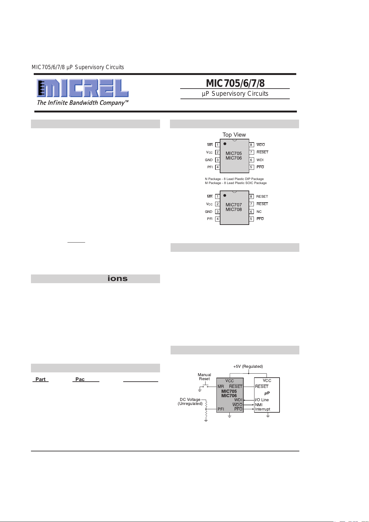
8
7
6
5
WDO
RESET
WDI
PFO
MIC705
MIC706
MR
PFO
1
2
3
4
V
CC
GND
PFI
8
7
6
5
RESET
RESET
NC
PFO
MIC707
MIC708
MR
PFO
Top View
N Package - 8 Lead Plastic DIP Package
M Package - 8 Lead Plastic SOIC Package
Part Package Temp. Range
MIC70_N 8-Lead PDIP -40°C to +85°C
MIC70_M 8-Lead SOIC -40°C to +85°C
·
Automotive Systems
·
Intelligent Instruments
·
Critical Microprocessor Power Monitoring
·
Printers
·
Computers
·
Controllers
·
Debounced Manual Reset Input is
TTL/CMOS Compatible
·
Reset Pulse Width, 200ms
·
Watchdog Timer, 1.6s (MIC705/MIC706)
·
4.4V or 4.65V Precision Voltage Monitor
·
Early Power Fail Warning or Low Battery
Detect
V
CC
RESET
µP
RESET
V
CC
MIC705
MIC706
+5V (Regulated)
MR
WDI
I/O Line
PFO InterruptPFI
DC Voltage
(Unregulated)
Manual
Reset
WDO
NMI
Typical Operating Circuit
Features
Description Pin Configuration
Ordering Information
Typical Applications
MIC705/6/7/8 µP Supervisory Circuits
MIC705/6/7/8
µP Supervisory Circuits
Page 2
MIC705/6/7/8 µP Supervisory Circuits
2
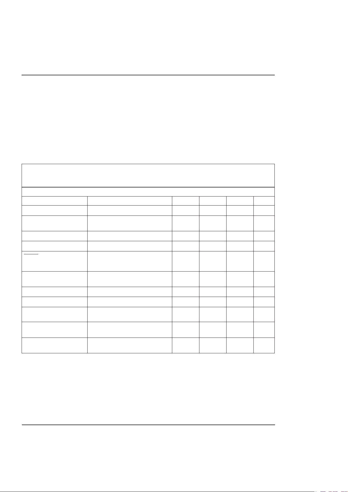
Electrical Characteristics
VCC= 4.75V to 5.5V for MIC705/MIC707, VCC= 4.5V to 5.5V for MIC706/MIC708, TA= -40°C to 85°C unless otherwise noted.
Parameter Conditions Min Typ Max Units
Operating Voltage Range, V
CC
MIC70-- 1.4 5.5 V
Supply Current MIC70-- 60 µA
Reset Voltage Threshold MIC705, MIC707 4.50 4.65 4.75 V
MIC706, MIC708 4.25 4.4 4.5
Reset Threshold Hysteresis 40 mV
Reset Pulse Width, t
RS
140 200 280 ms
RESET Output Voltage I
Source
= 800µA
VCC- 1.5V
V
I
Sink
= 3.2mA 0.4
MIC70--C, I
Sink
= 50µA, V
CC
= 1.4V 0.3
RESET Output Voltage I
Source
= 800µA
VCC- 1.5V
V
I
Sink
= 1.2mA 0.4
Watchdog Timeout Period, t
WD
1.0 1.6 2.25 sec
WDI Minimum Input Pulse, t
WP
VIL= 0.4V, VIH= 80% of V
CC
50 ns
WDI Threshold Voltage V
IH, VCC
= 5V
3.5
V
V
IL, VCC
= 5V 0.8
WDI Input Current WDI = 0V -150 -50 µA
WDI = V
CC
50 150
WDO Output Voltage I
Source
= 800µA
VCC- 1.5V
V
I
Sink
= 1.2mA 0.4
Absolute Maximum Ratings
Terminal Voltage
VCC. . . . . . . . . . . . . . . . . . . . . . . . . . . -0.3V to 6.0V
All Other Inputs . . . . . . . . . . . . -0.3V to (VCC+ 0.3V)
Input Current
V
CC,
Gnd. . . . . . . . . . . . . . . . . . . . . . . . . . . . . 25mA
Output Current (all outputs) . . . . . . . . . . . . . . . . . 20mA
Operating Temperature Range
MIC70_N, MIC70_M . . . . . . . . . . . . . . . . . -40°C to 85°C
Storage Temperature Range . . . . . . . . . . . . .-65°C to 150°C
Lead Temperature (Soldering - 10 sec.) . . . . . . . . . . . 300°C
Power Dissipation (PDIP) . . . . . . . . . . . . . . . . . . . . 475mW
Power Dissipation (SOIC) . . . . . . . . . . . . . . . . . . . . 400mW
Stresses above those listed under ABSOLUTE MAXIMUM RATINGS may cause permanent device failure. Functionality at or above these limits is not implied. Exposure to absolute
maximum ratings for extended periods may affect device reliability. Operating ranges define those limits between which the functionality of the device is guaranteed.
Page 3
MIC705/6/7/8 µP Supervisory Circuits
3
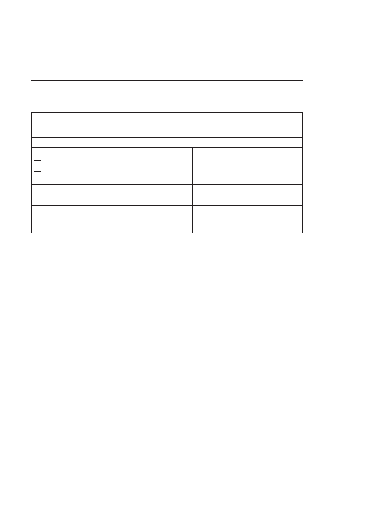
Electrical Characteristics
VCC= 4.75V to 5.5V for MIC705/MIC707, VCC= 4.5V to 5.5V for MIC706/MIC708, TA= -40°C to 85°C unless otherwise noted.
Parameter Conditions Min Typ Max Units
MR Pull-Up Current MR = 0V 100 250 600 µA
MR Pulse Width, t
MR
150 nS
MR Input Threshold V
IL
0.8 V
V
IH
2.0
MR to Reset Output Delay, t
MD
250 nS
PFI Input Threshold VCC= 5V 1.2
1.25
1.3 V
PFI Input Current
-25
0.01 +25 nA
PFO Output Voltage I
Sink
= 3.2mA 0.4 V
VCC= 5V, I
Source
= 800µA
VCC- 1.5V
Page 4

4
Manual Reset Input forces RESET to assert when pulled below 0.8V.
An internal pull-up current of 250µA on this input forces it high when left
floating. This input can also be driven from TTL or CMOS logic.
Primary supply input, +5V.
IC ground pin, 0V reference.
Power fail input. Internally connected to the power fail comparator
which is referenced to 1.25V. The power fail output (PFO) remains
high if PFI is above 1.25V. PFI should be connected to GND or V
OUT
if the power fail comparator is not used.
Power fail output. The power fail comparator is independent of all other
functions on this device.
Watchdog input. The WDI input monitors microprocessor activity, an
internal watchdog timer resets itself with each transition on the
watchdog input. If the WDI pin is held high or low for longer than the
watchdog timeout period, WDO is forced to active low. The watchdog
function can be disabled by floating the WDI pin.
No Connect
RESET is asserted if either VCCgoes below the reset threshold or by a
low signal on the manual reset input (MR). RESET remains asserted
for one reset timeout period (200ms) after VCCexceeds the reset
threshold or after the manual reset pin transitions from low to high. The
watchdog timer will not assert RESET unless WDO is connected to
MR.
Output for the watchdog timer. The watchdog timer resets itself with
each transition on the watchdog input. If the WDI pin is held high or
low for longer than the watchdog timeout period, WDO is forced low.
WDO will also be forced low if VCCis below the reset threshold and
will remain low until VCCreturns to a valid level.
RESET is the compliment of RESET and is asserted if either VCCgoes
below the reset threshold or by a low signal on the manual reset input
(MR). RESET is suitable for microprocessors systems that use an
active high reset.
Pin No.
MIC705 MIC707
Pin Name MIC706 MIC708
MR 11
VCC 22
GND 33
PFI 44
PFO 55
WDI 6 N/A
N/C N/A 6
RESET 77
WDO 8 N/A
RESET N/A 8
Pin Functions
MIC705/6/7/8 µP Supervisory Circuits
Page 5

5
+
-
4.65V*
RESET
GENERATOR
+
-
1.25V
WATCHDOG
TIMER
VCC(2)
MR (1)
PFO (5)
RESET (7)
WDO (8)
WDI (6)
PFI (4)
V
CC
250¥A
+
-
4.65V*
RESET
GENERATOR
+
-
1.25V
VCC(2)
MR (1)
PFO (5)
RESET (7)
PFI (4)
V
CC
RESET (8)
250µA
Figure 1. MIC705/MIC706 Block Diagram
Figure 2. MIC707/MIC708 Block Diagram
Block Diagram
* 4.4V for MIC706
* 4.4V for MIC708
MIC705/6/7/8 µP Supervisory Circuits
Page 6

6
The output of the watchdog timer (WDO) will remain
high if WDI sees a valid transition within the watchdog
timeout period or if WDI is left floating. If VCCfalls
below the reset threshold voltage then WDO goes low
immediately regardless of WDI. Thus, if WDI is left
floating, then WDO can be used as a low line indicator.
Microprocessor Reset
The RESET pin is asserted whenever V
CC
falls below
the reset threshold voltage or when MR goes low. The
reset pin remains asserted for a period of 200ms after
VCChas risen above the reset threshold voltage and
MR goes high. The reset function ensures the
microprocessor is properly reset and powers up into a
known condition after a power failure. RESET will
remain valid with VCCas low as 1.4V.
Power Fail Warning
An additional comparator which is independent of other
functions on the MIC705/706/707/708 is provided for
early warning of power failure. An external voltage
divider can be used to compare unregulated DC to an
internal 1.25V reference. The voltage divider ratio on
the input of the power fail comparator (PFI) can be
chosen so as to trip the power fail comparator a few
milliseconds before V
CC falls below the maximum reset
threshold voltage. The output of the power fail
comparator (PFO) can be used to interrupt the
microprocessor when used in this mode and execute
shut-down procedures prior to power loss.
Watchdog Timer
The microprocessor can be monitored by connecting
the WDI pin (watchdog input) to a bus line or I/O line. If
a transition doesn’t occur on the WDI pin within the
watchdog timeout period, then WDO will go low. A
minimum pulse of 50ns or any transition low-to-high or
high-to-low on the WDI pin will reset the watchdog timer.
+
-
1.25V
R1
R2
Unregulated DC
PFO
PFI
Figure 3. Power Fail Comparator
Circuit Description
Figure 4. Reset Timing Diagram
V
CC
MR
RESET
V
RT
t
MR
t
MD
t
RS
t
RS
WDO
MIC705/6/7/8 µP Supervisory Circuits
Page 7

7
MIC Direct
Industry P/N
Replacement
MAX705CPA MIC705N
MAX705CSA MIC705M
MAX705EPA MIC705N
MAX705ESA MIC705M
ADM705AN MIC705N
DS1705EPA MIC705N
DS1705ESA MIC705M
MAX706CPA MIC706N
MAX706CSA MIC706M
MAX706EPA MIC706N
ADM706AN MIC706N
DS1706EPA MIC706N
DS1706ESA MIC706M
MAX707CPA MIC707N
MAX707CSA MIC707M
MAX707EPA MIC707N
MAX707ESA MIC707M
ADM707AN MIC707N
DS1707EPA MIC707N
DS1707ESA MIC707M
MAX708CPA MIC708N
MAX708CSA MIC708M
MAX708EPA MIC708N
MAX708ESA MIC708M
ADM708AN MIC708N
DS1708EPA MIC708N
DS1708ESA MIC708M
Alternate Source Cross Reference Guide
MIC705/6/7/8 µP Supervisory Circuits
Page 8

8
Packaging Information
0.244
0.228
0.155
0.150
0.197
0.190
0.019
0.013
0.060
0.040
0.069
0.053
0.011
0.004
0.012
0.009
0.050
0.016
0-8¼
Pin 1Identifier
0.260
0.240
0.400
0.370
0.023
0.015
0.110
0.090
0.150
0.120
0.150
0.125
0.035
0.015
0.370
0.300
0.310
0.290
M Package, 8-Pin Small Outline
N Package, 8-Pin Plastic Dual-In-Line
MIC705/6/7/8 µP Supervisory Circuits
 Loading...