

Page 1
MIC6211 Micrel
MIC6211
IttyBitty™ Operational Amplifier
Preliminary Information
General Description
The MIC6211 IttyBitty™ op amp is a general-purpose, highperformance, single- or split-supply, operational amplifier in
a space-saving, surface-mount package.
The MIC6211 operates from 4V to 32V, single or differential
(split) supply. The input common-mode range includes ground.
The device features a 2.5MHz unity gain bandwidth, 6V/µs
slew rate, and is internally unity-gain compensated.
Inputs are protected against reverse polarity (input voltage
less than V–) and ESD (electrostatic discharge). Output is
current limited for both sourcing and sinking. Output short
circuits of unlimited duration are allowed, provided the power
dissipation specification is not exceeded.
The MIC6211 is available in the tiny, 5-lead SOT-23-5 surface-mount package.
Features
• 4V to 32V operation
• Small footprint package
• Unity gain stable
• 2.5 MHz unity gain bandwidth
• 6V/µs typical slew rate
• Short circuit protected
Applications
• Analog blocks
• Active filtering
Ordering Information
Part Number Temperature Range Package
MIC6211BM5 –40°C to +85°C SOT-23-5
Pin Configuration
V–
2
A11
OUT
13
Part
Identification
V+IN–
IN+
45
Pin Description
Pin Number Pin Name Pin Function
1 OUT Amplifier Output
2V– Negative Supply: Negative supply for split supply application or ground for
3 IN+ Noninverting Input
4IN– Inverting Input
5 V+ Positive Supply
Functional Configuration
single supply application.
V–
OUT
13
2
V+IN–
IN+
45
SOT-23-5 (M5)
Micrel, Inc. • 1849 Fortune Drive • San Jose, CA 95131 • USA • tel + 1 (408) 944-0800 • fax + 1 (408) 944-0970 • http://www.micrel.com
June 1999 1 MIC6211
Page 2

MIC6211 Micrel
Absolute Maximum Ratings
Supply Voltage (VV+ – VV–)............................. 36V or ±18V
Differential Input Voltage (V
Input Voltage (V
IN+
, V
IN–
– V
IN+
)..................... (VV– – 0.3V) to V
Output Short Circuit Current Duration ...............................∞
) .......................±36V
IN–
Operating Ratings
Supply Voltage .................................................... 4V to 32V
Ambient Temperature Range..................... –40°C to +85°C
SOT-23-5 Thermal Resistance (θJA).....................220°C/W
V+
(mounted to printed circuit board)
Electrical Characteristics (Differential Supply)
V+ = +15V, V– = –15V, VCM = 0V; RL = 2kΩ; TA = 25°C, bold values indicate –40°C ≤ TA ≤ +85°C, TA = TJ; unless noted
Symbol Parameter Condition Min Typ Max Units
V
OS
TCV
OS
I
B
I
OS
V
CM
CMRR Common Mode Rejection Ratio VCM = +13.5V, –15.0V 65 100 dB
PSRR Power Supply Rejection Ratio VS = ±2.5V to ±15V 65 110 dB
A
VOL
V
OUT
B
W
S
R
I
SC
I
S
Input Offset Voltage 27mV
Average Input Offset Drift Note 1 7 µV/°C
Input Bias Current 50 250 nA
Input Offset Current 830nA
Input Voltage Range +13.5 +13.8 V
–15.0 –15.3 V
Large Signal Voltage Gain VO = ±10V 25 180 V/mV
Maximum Output Voltage Swing ±12.5 ±14 V
Bandwidth 2.5 MHz
Slew Rate 6V/µs
Output Short Circuit Current Sourcing or sinking 30 50 mA
Supply Current 1.3 2.0 mA
Electrical Characteristics (Single Supply)
V+ = +5V, V– = 0V, VCM = 0.1V; TA = 25°C, bold values indicate –40°C ≤ TA ≤ +85°C, TA = TJ; unless noted
Symbol Parameter Condition Min Typ Max Units
V
OS
TCV
OS
I
B
I
OS
V
CM
CMRR Common Mode Rejection Ratio VCM = 0V to 3.5V 45 70 dB
PSRR Power Supply Rejection Ratio VS = ±2.5V to ±15V 65 105 dB
A
VOL
V
OUT
I
SC
I
S
General Note: Devices are ESD protected; however, handling precautions are recommended.
Note 1: Not production tested.
Input Offset Voltage 27mV
Average Input Offset Drift Note 1 7 µV/°C
Input Bias Current 65 250 nA
Input Offset Current 830nA
Input Voltage Range +3.5 +3.7 V
0 –0.3 V
Large Signal Voltage Gain VO = 1.5V to 3.5V, RL = 2k 15 170 V/mV
Maximum Output Voltage Swing RL = 10k to GND +3.8 +4.0 V
RL = 10k to +5V +1.0 +1.2 V
Output Short Circuit Current Sourcing or sinking 20 40 mA
Supply Current 1.2 1.8 mA
MIC6211 2 June 1999
Page 3
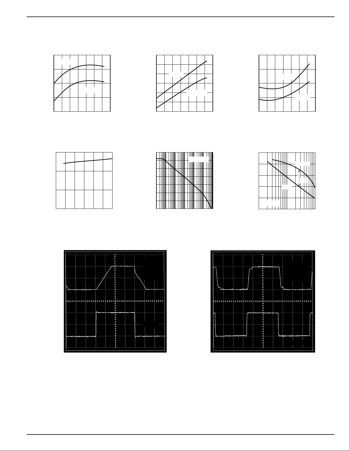
MIC6211 Micrel
0
5
10
15
20
-40 -20 0 20 40 60 80 100
INPUT OFFSET CURRENT (nA)
TEMPERATURE (°C)
Input Offset Current
vs. Temperature
VS = ±15V
VS = 5V
-20
-10
0
10
20
30
270
225
180
135
90
45
0.1 1.0 10
VOLTAGE GAIN (dB)
PHASE (°)
FREQUENCY (MHz)
GAIN
PHASE
Gain and Phase
vs. Frequency
VS = ±15V
72°
GND
+50mV
–50mV
INPUT VOLTAGE OUTPUT VOLTAGE
Small-Signal Transient Response
–50mV
GND
+50mV
AV = +1
RL = 2k
CL = 100pF
VS = ±15V
500ns/DIV
Typical Characteristics
Supply Current
1.4
1.3
1.2
1.1
SUPPLY CURRENT (mA)
1.0
vs. Temperature
VS = ±15V
VS = 5V
-40 -20 0 20 40 60 80 100
TEMPERATURE (°C)
Supply Current
vs. Supply Voltage
1.5
1.0
0.5
SUPPLY CURRENT (mA)
0
0 5 10 15 20 25 30
SUPPLY VOLTAGE (V)
Input Bias Current
vs. Temperature
90
80
70
60
50
40
INPUT BIAS CURRENT (nA)
30
VS = 5V
VS = ±15V
-40 -20 0 20 40 60 80 100
TEMPERATURE (°C)
Voltage Gain
0
0.01
vs. Frequency
VS = ±15V
1
0.1
FREQUENCY (kHz)
10
100
120
100
80
60
40
20
VOLTAGE GAIN (dB)
-20
1,000
10,000
+10V
GND
–10V
+10V
GND
–10V
INPUT VOLTAGE OUTPUT VOLTAGE
June 1999 3 MIC6211
Large-Signal Transient Response
AV = +1
RL = 2k
CL = 10pF
VS = ±15V
2µs/DIV
Page 4

MIC6211 Micrel
NOISE VOLTAGE (5µV/DIV)
Wideband Noise
VS = ±15V
5ms/DIV
Large-Signal
Frequency Response
30
25
20
15
10
5
0
10 100 1000 3000
PEAK-TO-PEAK OUTPUT VOLTAGE (V)
FREQUENCY (kHz)
VS = ±15V
R
= 2k
L
T
= 25°C
A
Common Mode Rejection Ratio
110
100
90
80
CMRR (dB)
70
60
50
vs. Frequency
VS = ±15V
0.01 0.1 1 10 100 1000
FREQUENCY (kHz)
Short Circuit Current
vs. Temperature
65
60
55
50
45
SHORT CIRCUIT CURRENT (mA)
40
-40 -20 0 20 40 60 80 100
TEMPERATURE (°C)
VS = ±15V
Power Supply Rejection
Ratio vs. Frequency
130
120
110
100
90
-PSRR
80
PSRR (dB)
70
60
50
0.001 0.01 0.1 1 10 100
FREQUENCY (kHz)
VS = ±15V
+PSRR
NOISE VOLTAGE (4µV/DIV)
0.1Hz to 10Hz Noise
VS = ±15V
1s/DIV
MIC6211 4 June 1999
Page 5

MIC6211 Micrel
Functional Diagram
V+
5
20Ω
V
20Ω
OUT
1
2
V–
(GND)
–IN
+IN
4
3
MIC6211
C
C
June 1999 5 MIC6211
Page 6

MIC6211 Micrel
-20
-10
0
10
20
30
1
10
100
1,000
10,000
100,000
V
OUT
(dB)
FREQUENCY (Hz)
1101k
100k
Applications Information
Common-Mode Range and Output Voltage
The input common-mode range of the MIC6211 is from the
negative supply voltage
voltage
. The output voltage swings within 1V of the positive
and negative supply voltage.
Voltage Buffer
Figure 1 shows a standard voltage follower/buffer. The output
voltage equals the input voltage. This circuit is used to buffer
a high impedance signal source. This circuit works equally
well with single or split supplies.
V
IN
Figure 1. Voltage Buffer
Inverting Amplifier
Figure 2 shows an inverting amplifier with its gain set by the
ratio of two resistors. This circuit works best with split supplies, but will perform with single supply systems if the noninverting input (+ input) is biased up above ground.
V
IN
Figure 2. Inverting Amplifer
Voltage Controlled Current Sink
Figure 3 is a voltage controlled current sink. A buffer transistor forces current through a programming resistor until the
feedback loop is satisfied. Current flow is VIN/R. This circuit
works with single or split supplies.
to
1.2V below the positive supply
3
1
4
V
= V
OUT
IN
R1
R2
4
3
V
OUT
V
IN
3
4
V
OUT
1
1
V
OUT
R1
V
IN
R2
High-Pass Filter
Figure 4 is an active filter with 20dB (10×) gain and a lowfrequency cutoff of 10Hz. The high gain-bandwidth of the
MIC6211 allows operation beyond 100kHz. This filter configuration is designed for split supplies.
0.1µF
332k
1µF 1µF
IN
7.5k
4
1
3
V
OUT
Figure 4a. High-Pass Filter
Figure 4b. High-Pass Filter Response
Summing Amplifier
Figure 5 is a single supply summing amplifier. In this configuration, the output voltage is the sum of V1 and V2, minus the
sum of V3 and V4. By adding more resistors to either the
inverting or non-inverting input, more voltages may be
summed. This single supply version has one important restriction: the sum of V1 and V2 must exceed the sum of V3
and V4, since the output voltage cannot pull below zero with
only a single supply.
R
V1
R
V2
R
V3
R
V4
All resistors are equal.
V
= V1 + V2 – V3 – V4
OUT
V1 + V2 > V3 + V4 for single supply operation
3
R
4
1
R
V
OUT
Figure 5. Summing Amplifier
V
IN
I
R
R
Figure 3. Voltage Controlled Current Sink
MIC6211 6 June 1999
Page 7

MIC6211 Micrel
Package Information
1.90 (0.075) REF
0.95 (0.037) REF
3.02 (0.119)
2.80 (0.110)
0.50 (0.020)
0.35 (0.014)
1.75 (0.069)
1.50 (0.059)
1.30 (0.051)
0.90 (0.035)
0.15 (0.006)
0.00 (0.000)
SOT-23-5 (M5)
3.00 (0.118)
2.60 (0.102)
10°
0°
DIMENSIONS:
MM (INCH)
0.20 (0.008)
0.09 (0.004)
0.60 (0.024)
0.10 (0.004)
June 1999 7 MIC6211
Page 8

MIC6211 Micrel
MICREL INC. 1849 FORTUNE DRIVE SAN JOSE, CA 95131 USA
TEL + 1 (408) 944-0800 FAX + 1 (408) 944-0970 WEB http://www.micrel.com
This information is believed to be accurate and reliable, however no responsibility is assumed by Micrel for its use nor for any infringement of patents or
other rights of third parties resulting from its use. No license is granted by implication or otherwise under any patent or patent right of Micrel Inc.
© 1999 Micrel Incorporated
MIC6211 8 June 1999
 Loading...