

Datasheet MIC5237-3.3BT, MIC5237-3.3BU, MIC5237-5.0BT, MIC5237-2.5BU, MIC5237-5.0BU Datasheet (MICREL)
...Page 1
MIC5237 Micrel
MIC5237
500mA Low-Dropout Regulator
Preliminary Information
General Description
The MIC5237 is a general-purpose low-dropout regulator
capable of 500mA output current with better than 3% output
voltage accuracy. Using Micrel’s proprietary Super
ßeta PNP™ process with a PNP pass element, these regulators feature less than 300mV dropout voltage and typically
8mA ground current at full load.
Designed for applications that require moderate current over
a broad input voltage range, including hand-held and batterypowered devices, the MIC5237 is intended for applications
that can tolerate moderate voltage drop at higher current.
Key features include low ground current to help prolong
battery life, reversed-battery protection, current limiting, overtemperature shutdown, and thermally efficient packaging.
The MIC5237 is available in fixed output voltages only.
For space-critical applications and improved performance,
see the MIC5209 and MIC5219. For output current requirements up to 750mA, see the MIC2937.
Ordering Information
Features
• Guaranteed 500mA output over the full operating
temperature range
• Low 300mV typical dropout voltage at full load
• Extremely tight load and line regulation
• Current and thermal limiting
• Reversed-battery protection
• TO-220 and TO-263 packages
• Low temperature coefficient
• No-load stability
• Low-noise output
Applications
• Portable and laptop computers
• Desktop computer
• Battery chargers
• SMPS post-regulator/dc-to-dc modules
• Consumer and personal electronics
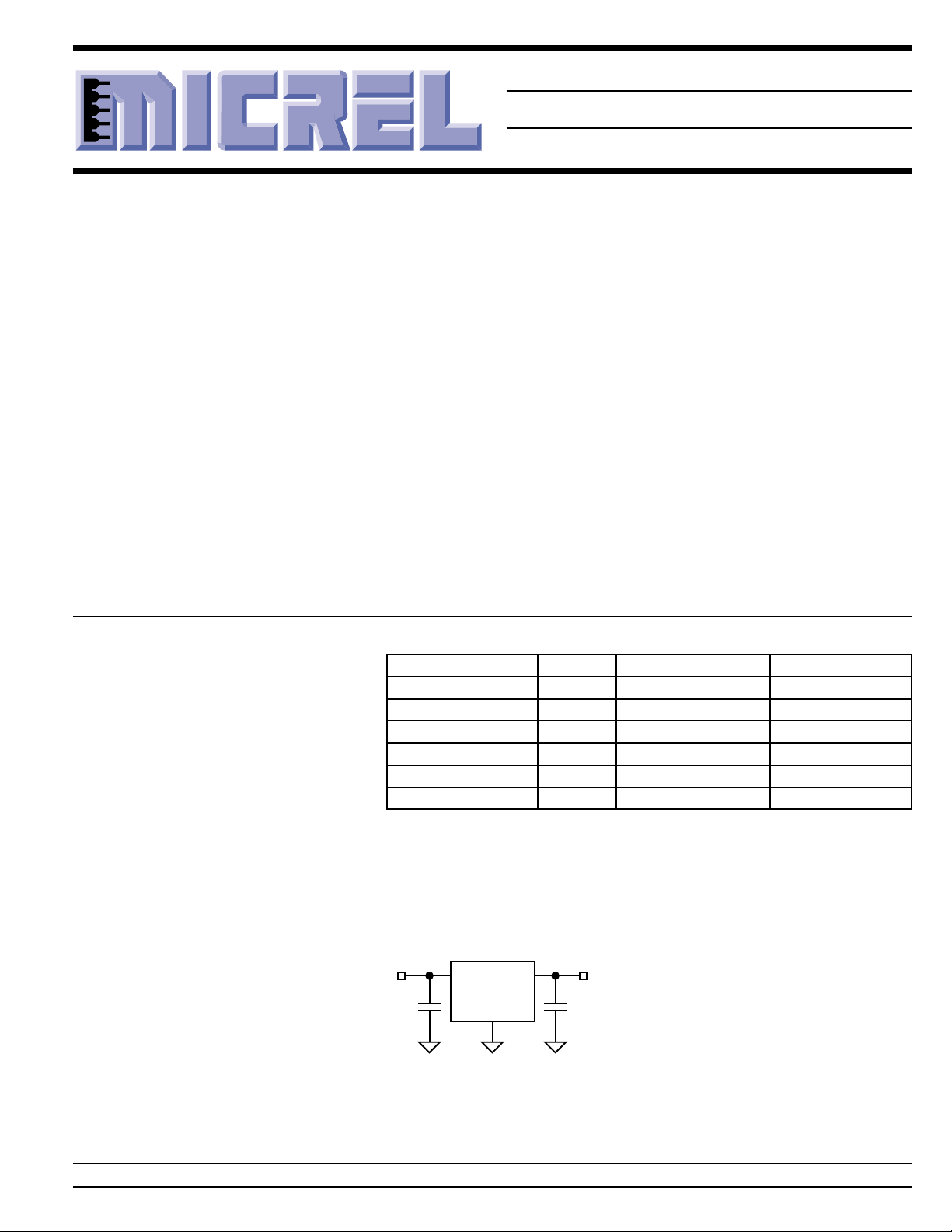
Typical Application
Part Number Voltage Junct. Temp. Range Package
MIC5237-2.5BT 2.5V –40°C to +125°C TO-220
MIC5237-2.5BU 2.5V –40°C to +125°C TO-263
MIC5237-3.3BT 3.3V –40°C to +125°C TO-220
MIC5237-3.3BU 3.3V –40°C to +125°C TO-263
MIC5237-5.0BT 5.0V –40°C to +125°C TO-220
MIC5237-5.0BU 5.0V –40°C to +125°C TO-263
V
IN
≥5.6V
1.0µF
MIC5237-5.0
IN OUT
GND
V
OUT
5.0V ±3%
1.0µF
tantalum
Micrel, Inc. • 1849 Fortune Drive • San Jose, CA 95131 • USA • tel + 1 (408) 944-0800 • fax + 1 (408) 944-0970 • http://www.micrel.com
January 2000 1 MIC5237
Page 2
MIC5237 Micrel
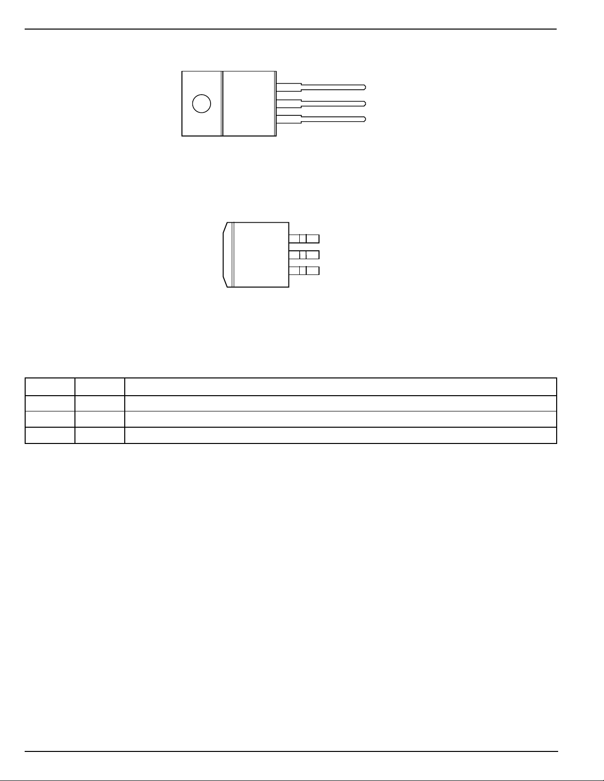
Pin Configuration
3 OUT
TAB
MIC5237-x.xBT
TAB
(TO-220-3)
3 OUT
2 GND
1IN
2 GND
1IN
MIC5237-x.xBU
(TO-263-3)
Pin Description
Pin No. Pin Name Pin Function
1 IN Supply Input
2, TAB GND Ground: TO-220 and TO-263 pin 2 and TAB are internally connected.
3 OUT Regulator Output
Absolute Maximum Ratings
Input Voltage (VIN) ........................................ –20V to +20V
Power Dissipation (PD) ............................Internally Limited
Junction Temperature (TJ) .......................–40°C to +125°C
Lead Temperature (soldering, 5 sec.) ....................... 260°C
Operating Ratings
Input Voltage (VIN) ....................................... +2.5V to +16V
Junction Temperature (TJ) .......................–40°C to +125°C
Package Thermal Resistance
TO-220 (θJA) .......................................................55°C/W
TO-220 (θJC) .........................................................3°C/W
TO-263 (θJC) .........................................................3°C/W
MIC5237 2 January 2000
Page 3
MIC5237 Micrel
Electrical Characteristics
VIN = V
Symbol Parameter Conditions Min Typical Max Units
V
OUT
∆V
OUT
∆V
OUT/VOUT
∆V
OUT/VOUT
V
– V
IN
I
GND
PSRR Ripple Rejection f = 120Hz 75 dB
I
LIMIT
∆V
OUT
e
no
Note 1: Absolute maximum ratings indicate limits beyond which damage to the component may occur. Electrical specifications do not apply when
Note 2: Output voltage temperature coefficient is defined as the worst case voltage change divided by the total temperature range.
Note 3: Regulation is measured at constant junction temperature using low duty cycle pulse testing. Parts are tested for load regulation in the load
Note 4: Dropout voltage is defined as the input to output differential at which the output voltage drops 2% below its nominal value measured at 1V
Note 5: Ground pin current is the regulator quiescent current plus pass transistor base current. The total current drawn from the supply is the sum of
Note 6: Thermal regulation is defined as the change in output voltage at a time “t” after a change in power dissipation is applied, excluding load or line
+ 1.0V; C
OUT
Output Voltage Accuracy variation from nominal V
= 4.7µF, I
OUT
= 100µA; TJ = 25°C, bold values indicate –40°C ≤ TJ ≤ +125°C; unless noted.
OUT
OUT
–3 3 %
–5 5 %
/∆T Output Voltage Note 2 40 ppm/°C
Temperature Coefficient
Line Regulation VIN = V
+ 1V to 16V 0.05 %/V
OUT
0.015 0.1 %/V
Load Regulation I
= 100µA to 500mA, Note 3 0.05 0.5 %
OUT
0.7 %
OUT
Dropout Voltage, Note 4 I
= 100µA1070mV
OUT
90 mV
I
= 50mA 115 190 mV
Ground Pin Current, Note 5 I
OUT
= 150mA 165 350 mV
I
OUT
= 500mA 300 600 mV
I
OUT
= 100µA80130µA
OUT
I
= 50mA 350 650 µA
OUT
280 mV
450 mV
700 mV
170 µA
900 µA
I
= 150mA 1.8 2.5 mA
OUT
3.0 mA
I
= 500mA 8 15 mA
OUT
20 mA
Current Limit V
= 0V 700 900 mA
OUT
1000
/∆P
Thermal Regulation Note 6 0.05 %/W
D
Output Noise V
operating the device outside of its operating ratings. The maximum allowable power dissipation is a function of the maximum junction
temperature, T
dissipation at any ambient temperature is calculated using: P
tion will result in excessive die temperature, and the regulator will go into thermal shutdown. See the “Thermal Considerations” section for
details.
range from 100µA to 500mA. Changes in output voltage due to heating effects are covered by the thermal regulation specification.
differential.
the load current plus the ground pin current.
regulation effects. Specifications are for a 500mA load pulse at VIN = 16V for t = 10ms.
, the junction-to-ambient thermal resistance, θJA, and the ambient temperature, TA. The maximum allowable power
J(max)
C
OUT
OUT
= 5.0V, I
= 2.2µF
D(max)
= 50mA, 500
OUT
= (T
J(max)–TA
) ÷ θJA. Exceeding the maximum allowable power dissipa-
nV/ Hz
January 2000 3 MIC5237
Page 4

MIC5237 Micrel
Block Diagram
V
IN
IN
Bandgap
Ref.
Current Limit
Thermal Shutdown
MIC5237-x.x
GND
OUT
V
OUT
C
OUT
Fixed Regulator
MIC5237 4 January 2000
Page 5

MIC5237 Micrel
-100
-80
-60
-40
-20
0
1E+11E+21E+3 1E+41E+51E+61E+7
PSRR (dB)
FREQUENCY (Hz)
Power Supply
Rejection Ratio
I
OUT
= 100mA
C
OUT
= 1µF
VIN = 6V
V
OUT
= 5V
10
100
1k
10k
100k
1M
10M
0
10
20
30
40
50
60
0 0.1 0.2 0.3 0.4
RIPPLE REJECTION (dB)
VOLTAGE DROP (V)
√
Typical Characteristics
Power Supply
Rejection Ratio
0
-20
-40
-60
PSRR (dB)
-80
-100
1E+11E+21E+3 1E+41E+51E+61E+7
10
1k
100
FREQUENCY (Hz)
10k
I
C
OUT
OUT
100k
VIN = 6V
V
= 5V
OUT
= 100µA
= 1µF
1M
10M
Power Supply
Rejection Ratio
0
-20
-40
-60
PSRR (dB)
-80
-100
1E+11E+21E+3 1E+41E+51E+61E+7
10
1k
100
FREQUENCY (Hz)
10k
I
C
OUT
OUT
100k
VIN = 6V
V
= 5V
OUT
= 1mA
= 1µF
1M
Power Supply Ripple Rejection
vs. Voltage Drop
1mA
10mA
I
= 100mA
OUT
C
= 1µF
OUT
10M
Noise Performance
10
1
Hz)
0.1
0.01
NOISE (µV/
V
= 5V
OUT
0.001
C
= 10µF
OUT
electrolytic
0.0001
10
1E+11E+21E+3 1E+41E+51E+61E+7
1k
100
FREQUENCY (Hz)
100mA
1mA
10k 100k1M10M
10mA
January 2000 5 MIC5237
Page 6

MIC5237 Micrel
Applications Information
The MIC5237 is intended for general-purpose use and can be
implemented in a wide variety of applications where 500mA
of output current is needed. It is available in several voltage
options for ease of use. For voltage options that are not
available on the MIC5237, consult the MIC5209 for a 500mA
adjustable LDO regulator, or the MIC5219 for applications
that require only short-duration peak output current.
Input Capacitor
A 1µF capacitor should be placed from IN to GND if there is
more than 10 inches of wire between the input and the ac filter
capacitor or if a battery is used as the input.
Output Capacitor
An output capacitor is required between OUT and GND to
prevent oscillation. 1µF minimum is recommended for standard applications. Larger values improve the regulator’s
transient response. The output capacitor value may be increased without limit.
The output capacitor should have an ESR (equivalent series
resistance) of about 5Ω or less and a resonant frequency
above 1MHz. Ultralow-ESR capacitors can cause low-amplitude oscillations and/or underdamped transient response.
Most tantalum or aluminum electrolytic capacitors are adequate; film types will work, but are more expensive. Since
many aluminum electrolytics have electrolytes that freeze at
about –30°C, solid tantalums are recommended for operation
below –25°C.
At lower values of output current, less output capacitance is
needed for output stability. The capacitor can be reduced to
0.47µF for current below 10mA or 0.33µF for currents below
1mA.
For 2.5V applications a 22µF output capacitor is recommended to reduce startup voltage overshoot.
No-Load Stability
The MIC5237 will remain stable and in regulation with no load
(other than the internal voltage divider) unlike many other
voltage regulators. This is especially important in CMOS
RAM keep-alive applications.
Thermal Considerations
Proper thermal design can be accomplished with some basic
design criteria and some simple equations. The following
information is required to implement a regulator design.
VIN = input voltage
V
= output voltage
OUT
I
= output current
OUT
TA = ambient operating temperature
I
= ground current
GND
The regulator ground current, I
from the data sheet. Assuming the worst case scenario is
good design procedure, and the corresponding ground cur-
, can be measured or read
GND
rent number can be obtained from the data sheet. First,
calculate the power dissipation of the device. This example
uses the MIC5237-5.0BT, a 13V input, and 500mA output
current, which results in 20mA of ground current, worst case.
The power dissipation is the sum of two power calculations:
voltage drop × output current and input voltage × ground
current.
P = (V – V ) I + V I
[]
DIN
P = [(13V – 5V) 500mA] + 13V 20mA
D
P = 4.260W
D
×
OUT OUT
××
×
()
IN
GND
()
From this number, the heat sink thermal resistance is determined using the regulator’s maximum operating junction
temperature (T
) and the ambient temperature (TA)
J(max)
along with the power dissipation number already calculated.
T
J(MAX)
= 125°C
θJC = junction-to-case thermal resistance
θCS = case-to-sink thermal resistance
θJA = junction-to-ambient thermal resistance
θSA = sink-to-ambient thermal resistance
To determine the heat sink thermal resistance, the junctionto-case thermal resistance of the device must be used along
with the case-to-heat sink thermal resistance. These numbers show the heat-sink thermal resistance required at TA =
25°C that does not exceed the maximum operating junction
temperature.
T T
θ
JA
θθθ
SA
J(max) A
=
=−
JA
−
P
D
JC
θCS is approximately 1°C/W and θJC for the TO-220 is 3°C/W
in this example.
θJA =
125 – 25
4.260W
θJA = 23.5 C/W°
θSA = 23.5 C/W – 3 C/W + 1 C/W°°°
()
θSA = 19.5 C/W°
Therefore, a heat sink with a thermal resistance of 19.5° C/W
will allow the part to operate safely and it will not exceed the
maximum junction temperature of the device. The heat sink
can be reduced by limiting power dissipation, by reducing the
input voltage or output current. Either the TO-220 or TO-263
package can operate reliably at 2W of power dissipation
without a heat sink. Above 2W, a heat sink is recommended.
For a full discussion on voltage regulator thermal effects,
please refer to “Thermal Management” in Micrel’s
with Low-Dropout Voltage Regulators
handbook.
Designing
MIC5237 6 January 2000
Page 7

MIC5237 Micrel
Package Information
0.151 D ±0.005
0.108 ±0.005
(2.74 ±0.13)
0.818 ±0.005
(20.78 ±0.13)
(3.84 D ±0.13)
0.410 ±0.010
(10.41 ±0.25)
0.356 ±0.005
(9.04 ±0.13)
0.176 ±0.005
(4.47 ±0.13)
0.590 ±0.005
(14.99 ±0.13)
0.050 ±0.005
(1.27 ±0.13)
7°
0.050 ±0.003
(1.27 ±.08)
0.065±0.010
20°±2°
0.100 ±0.005
(2.54 ±0.13)
0.405±0.005
(28.96 ±0.25)
0.030 ±0.003
(0.76 ±0.08)
3-Lead TO-220 (T)
0.050±0.005
0.360±0.005
0.600±0.025
1.140 ±0.010
0.018 ±0.008
(0.46 ±0.020)
7°
3°
0.100 ±0.020
(2.54 ±0.51)
DIMENSIONS:
0.176±0.005
0.050±0.005
SEATING PLANE
+0.004
0.004
–0.008
INCH
(MM)
0.100 BSC 0.050
DIM. = INCH
8° MAX
0.015 ±0.002
0.100±0.01
3-Lead TO-263 (U)
January 2000 7 MIC5237
Page 8

MIC5237 Micrel
MICREL INC. 1849 FORTUNE DRIVE SAN JOSE, CA 95131 USA
TEL + 1 (408) 944-0800 FAX + 1 (408) 944-0970 WEB http://www.micrel.com
This information is believed to be accurate and reliable, however no responsibility is assumed by Micrel for its use nor for any infringement of patents or
other rights of third parties resulting from its use. No license is granted by implication or otherwise under any patent or patent right of Micrel Inc.
© 2000 Micrel Incorporated
MIC5237 8 January 2000
 Loading...