

Page 1
MIC2775 Micrel
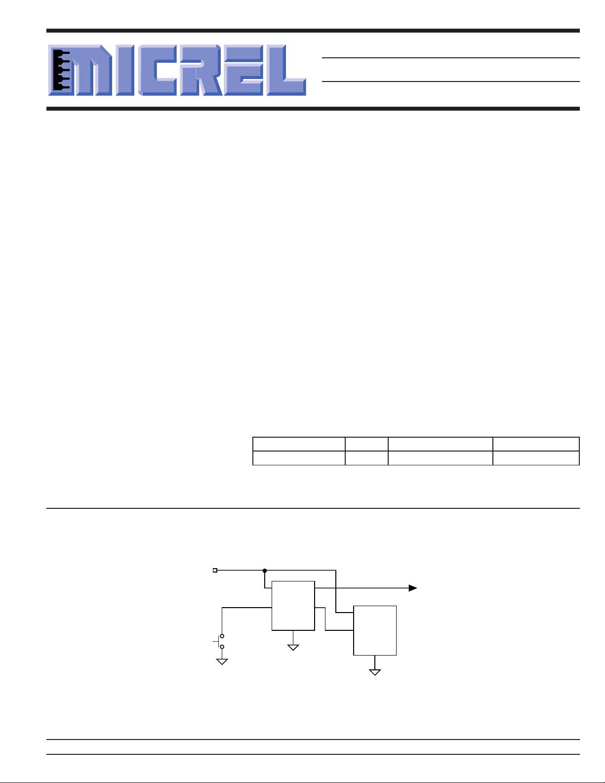
RST
/RST
VDD
/MR
GND
MIC2775-17
VDD
OTHER
LOGIC
/RESET
GND
MICROPROCESSOR
Manual
Reset
1.8V
MIC2775
Micro-Power Voltage Supervisor
Advance Information
General Description
The MIC2775 is a power supply supervisor that provides
under-voltage monitoring, manual reset capability, and poweron reset generation in a compact 5-pin SOT package. Features include an under-voltage detector, a delay generator, a
manual reset input, and both active-high and active-low reset
outputs. The under-voltage detector compares VDD against
a fixed threshold. Ten factory-programmed thresholds are
available.
The reset outputs are asserted for no less than 140ms at
power-on and any time the input voltage drops below the
reference voltage. It remains asserted for the timeout period
after the input voltage subsequently rises back above the
threshold boundary. A reset can be generated at any time by
asserting the manual reset input, /MR. This reset output will
remain active at least 140ms after the release of /MR. The
/MR input can also be used to daisy-chain the MIC2775 onto
existing power monitoring circuitry or other supervisors.
Hysteresis is included to prevent chattering due to noise.
Typical supply current is a low 3.5µA.
Features
• Monitors power supply for under-voltage conditions
• Choice of factory-programmed thresholds
• Generates 140ms (minimum) power-on RESET pulse
• Manual reset capability
• Both active-high and active-low RESET outputs
• /RST output valid down to 1.2V
• Ultra-low supply current, 3.5µA typical
• Rejects brief input transients
• No external components
• Pin compatible upgrade for MAX825
• IttyBitty™ 5-lead SOT-23 package
Applications
• Monitoring processor core and input/output voltages
• Computer systems
• PDAs, hand-held PCs
• Embedded controllers
• Telecommunications systems
• Power supplies
Ordering Information
Part Number Marking Junction Temp. Range Package
MIC2775-XXBM5 UJXX –40°C to +85°C SOT-23-5
Typical Application
IttyBitty™ is a trademark of Micrel, Inc.
September 29, 2000 1 MIC2775
Micrel, Inc. • 1849 Fortune Drive • San Jose, CA 95131 • USA • tel + 1 (408) 944-0800 • fax + 1 (408) 944-0970 • http://www.micrel.com
Page 2
MIC2775 Micrel
Standard Voltage Options*
Voltage Typical Nominal Threshold
Code Application (VDD) Voltage (VTH)
46 5.0V ±5% 4.68
44 5.0V ±10% 4.43
31 3.3V ±5% 3.09
29 3.3V ±10% 2.93
28 3.0V ±5% 2.81
26 2.85V ±5% 2.67
25 2.70V ±5% 2.53
23 2.5V ±5% 2.34
22 2.4V ±5% 2.25
17 1.8V ±5% 1.69
*There are ten standard versions available with an order increment of 3000 pieces. Samples of standard versions are
normally available from stock. Contact factory for information on non-standard versions. Available in tape-and-reel only.
Pin Configuration
Pin Description
Pin Number Pin Name Pin Function
1 RST Digital (Output): Asserted high whenever V
2 GND Ground
3 /RST Digital (Output): Asserted low whenever V
4 /MR Digital (Input): Driving this pin low initiates an immediate and unconditional
5 VDD Analog (Input): Power supply input and the voltage being monitored.
GND
2
/RST
13
VDD/MR
RST
45
SOT-23-5 (M5)
falls below the reference
voltage. It will remain asserted for no less than 140ms after V
DD
above the threshold limit.
falls below the reference
DD
voltage. It will remain asserted for no less than 140ms after V
above the threshold limit.
reset. Assuming V
high), the reset output will be de-asserted no less than 140ms later. /MR
is above the threshold when /MR is released (returns
DD
may be driven by a logic signal or a mechanical switch. /MR has an internal
pull-up to VDD and may be left open if unused.
returns
DD
returns
DD
MIC2775 2 September 29, 2000
Page 3
MIC2775 Micrel
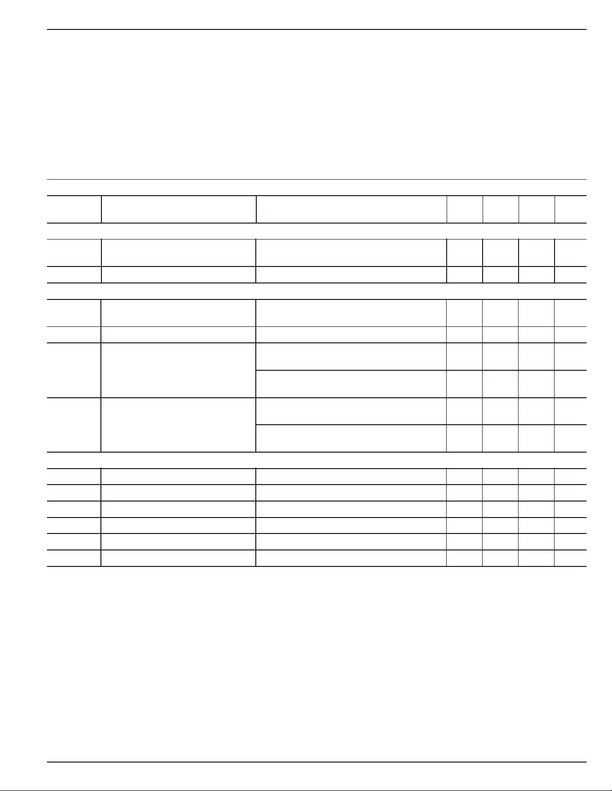
Absolute Maximum Ratings (Note 1)
Supply Voltage (V
Input Voltage (V
RST, (/RST) Current .................................................. 20mA
Storage Temperature (T
) ..................................... –0.3V to +7V
DD
) ....................................... –0.3V to +7V
/MR
) ....................... –65°C to +150°C
S
Operating Ratings (Note 2)
Supply Voltage (V
Input Voltage (V
Ambient Temperature Range (T
Package Thermal Resistance (θJA) ...................... 256°C/W
) .................................. +1.5V to +5.5V
DD
) .................................... –0.3V to +6.0V
/MR
) ............. –40°C to +85°C
A
ESD Rating, Note 3 ................................................... 1.5kV
Electrical Characteristics
Note 5; TA = +25°C, bold values indicate –40°C ≤ TA ≤ +85°C; unless noted
Symbol Parameter Condition Min Typ Max Units
I
DD
Supply Current VDD = V
open, Note 5
VDD VOLTAGE THRESHOLD
V
HYST
Under-Voltage Threshold On V
Hysteresis Voltage 1%
DD
RST, /RST OUTPUTS
t
PROP
Propagation Delay VDD = VTH + 1.5% + 100mV to 20 µs
VDD = VTH – 1.5% - 100 mV
t
RST
V
OL
Reset Pulse Width 140 280 ms
RST or /RST Output Voltage Low I
SINK
VDD ≥ 1.6V
I
SINK
VDD ≥ 1.2V; Note 4
V
OH
RST or /RST Output Voltage High I
SOURCE
VDD ≥ 1.5V
I
SOURCE
VDD ≥ 1.2V; Note 4
/MR INPUT
V
IH
V
IL
t
PROP
t
MIN
I
PU
I
IN
Note 1. Exceeding the absolute maximum rating may damage the device.
Note 2. The device is not guaranteed to function outside its operating rating.
Note 3. Devices are ESD sensitive. Handling precautions recommended. Human body model, 1.5k in series with 100pF.
Note 4. VDD operating range is 1.5V to 5.5V. Output is guaranteed to be asserted down to VDD = 1.2V.
Note 5. VDD equals nominal “ Typical Application (VDD)” as shown in “Standard Voltage Options Table.”
Input High Voltage 0.7V
Input Low Voltage 0.3V
Propagation Delay From V
Minimum Input Pulse Width Reset Occurs, V
Internal Pull-up Current 100 nA
Input Current, /MR V
/MR
+1.6%, /MR, RST, /RST 3.5 µA
TH
VTH–1.5%
V
THVTH
+1.5%
= 1.6mA; 0.3 V
= 100µA; 0.3 V
= 500µA; 0.8V
= 10µA; 0.8V
< (VIL –100mV) 5 µs
/MR
< V
/MR
IL
< V
IL
DD
DD
DD
DD
33 ns
100 nA
V
V
V
V
V
V
September 29, 2000 3 MIC2775
Page 4

MIC2775 Micrel
Timing Diagram
V
/MR
V
/RST
(ACTIVE LOW)
V
(ACTIVE HIGH)
RST
V
DD
0V
V
IH
V
IL
V
OH
V
OL
V
OH
V
OL
t
A
RST
A
> t
MIN
t
RST
t
RST
V
V
HYST
TH
Propagation delays not shown for clarity.
Note A. The MIC2775 ignores very brief transients.
See “Applications Information” for details.
MIC2775 4 September 29, 2000
Page 5

MIC2775 Micrel
Functional Diagram
V
DD
V
REF
V
DD
I
PU
/MR
GND
Functional Description
VDD Input
The VDD pin is both the power supply terminal and a monitored input voltage. The voltage at this pin is continually
compared against the internal reference. The trip-point at
which a reset occurs is factory programmed. A reset is
triggered if and when VDD falls below the trip-point. Hysteresis is employed to prevent chattering due to noise. The
comparator on the VDD input is relatively immune to very brief
negative-going transients.
RST, /RST Reset Outputs
Typically, the MIC2775 is used to monitor the power supply
of intelligent circuits such as microcontrollers and microprocessors. By connecting the appropriate reset output of a
MIC2775 to the reset input of a µC or µP, the processor will
be properly reset at power-on and during power-down and
brown-out conditions. In addition, asserting /MR, the manual
reset input, will activate the reset function.
Delay
Line
RSQ
One Shot
/Q
MIC2775
/RST
RST
The reset outputs are asserted any time /MR is asserted or if
VDD drops below the threshold voltage. The reset outputs
remain asserted for t
(min) after VDD subsequently returns
RST
above the threshold boundary and/or /MR is released. A reset
pulse is also generated at power-on. Hysteresis is included in
the comparator to prevent chattering of the outputs due to
noise.
/MR, Manual Reset Input
The ability to initiate a reset via external logic or a manual
switch is provided in addition to the MIC2775’s automatic
supervisory functions. Driving the /MR input to a logic low
causes an immediate and unconditional reset to occur.
Assuming VDD is within tolerance when /MR is released
(returns high), the reset outputs will be de-asserted no less
than t
later. /MR may be driven by a logic signal or
RST
mechanical switch. Typically, a momentary push-button switch
is connected such that /MR is shorted to ground when the
switch contacts close. The switch may be connected directly
between /MR and GND. /MR has an internal 100nA pull-up
current to VDD and may be left open if unused.
September 29, 2000 5 MIC2775
Page 6

MIC2775 Micrel
Application Information
Ensuring Proper Operation at Low Supply
At levels of VDD below 1.2V, the MIC2775’s /RST output
cannot turn on sufficiently to produce a valid logic-low on
/RST. In this situation, circuits driven by /RST could be
allowed to float, causing undesired operation. (In most cases,
however, it is expected that the circuits driven by the MIC2775
will be similarly inoperative at VDD ≤ 1.2V.)
If a given application requires that /RST be valid below V
= 1.2V, this can be accomplished by adding a pull-down
resistor to the /RST output. A value of 100kΩ is recommended as this is usually an acceptable compromise of
quiescent current and pull-down current. The resistor’s value
is not critical, however. See Figure 1.
V
CC
MIC2775-XX
/RST
VDD
RST
GND
/MR
Manual
Reset
MICROPROCESSOR
VCC
100k
/RESET
GND
DD
Transient response
The MIC2775 is inherently immune to very short negativegoing “glitches.” Very brief transients may exceed the voltage
threshold without tripping the output.
As shown in Figure 3, in general the narrower the transient,
the deeper the threshold overdrive that will be ignored by the
MIC2775. The graph represents the typical allowable transient duration for a given amount of threshold overdrive that
will not generate a reset.
Typical V
Transient Response
100
80
60
40
20
0
MAX. TRANSIENT DURATION (µs)
0 500 1000 1500 2000
RESET COMP. OVERDRIVE, V
DD
REF–VDD
(mV)
Figure 3. Typical VDD Transient Response
Figure 1. MIC2775 Valid /Reset Below 1.2V
The statements above also apply to the MIC2775’s RST
output. That is, to ensure valid RST signal levels at VDD <
1.2V, a pull-up resistor (as opposed to a pull-down) should be
added to the RST output. A value of 100kΩ is typical for this
application as well. See Figure 2.
V
CC
MIC2775-XX
/RST
VDD
RST
/MR GND
Manual
Reset
MICROPROCESSOR
VCC
/RESET
100k
Rpull-down
GND
Figure 2. MIC2775 Valid Reset Below 1.2V
MIC2775 6 September 29, 2000
Page 7

MIC2775 Micrel
Package Information
1.90 (0.075) REF
0.95 (0.037) REF
3.02 (0.119)
2.80 (0.110)
0.50 (0.020)
0.35 (0.014)
1.75 (0.069)
1.50 (0.059)
1.30 (0.051)
0.90 (0.035)
0.15 (0.006)
0.00 (0.000)
SOT-23-5 (M5)
3.00 (0.118)
2.60 (0.102)
10°
0°
DIMENSIONS:
MM (INCH)
0.20 (0.008)
0.09 (0.004)
0.60 (0.024)
0.10 (0.004)
MICREL INC. 1849 FORTUNE DRIVE SAN JOSE, CA 95131 USA
TEL + 1 (408) 944-0800 FAX + 1 (408) 944-0970 WEB http://www.micrel.com
This information is believed to be accurate and reliable, however no responsibility is assumed by Micrel for its use nor for any infringement of patents or
other rights of third parties resulting from its use. No license is granted by implication or otherwise under any patent or patent right of Micrel Inc.
© 2000 Micrel Incorporated
September 29, 2000 7 MIC2775
 Loading...