

Page 1
MIC2558 Micrel
MIC2558
PCMCIA Dual Card Socket VPP Switching Matrix
General Description
The MIC2558 Dual VPP Matrix switches the four voltages
required by PCMCIA (Personal Computer Memory Card
International Association) card V
PP1
and V
Pins. The
PP2
MIC2558 provides selectable 0V, 3.3V, 5.0V, or 12.0V (±5%)
from the system power supply to V
PP1
and V
. Output
PP2
voltage is selected by two digital inputs per VPP pin. Output
current ranges up to 120mA. Four output states, VPP, VCC,
high impedance, and active logic low are available, and V
is independent of V
. An auxiliary control input determines
PP2
PP1
whether the high impedance (open) state or low logic state is
asserted.
In standby mode or full operation, the device draws very little
quiescent current, typically less than 1µA.
The MIC2558 is available in a 14-pin SOIC and a 14-pin
plastic DIP.
Applications
• PCMCIA VPP Pin Voltage Switch
• Power Supply Management
Features
• Complete PCMCIA VPP Switch Matrix in a Single IC
• Dual Matrix allows independent V
PP1
and V
PP2
• Digital Selection of 0V, VCC, VPP, or High
Impedance Output
• No V
PPOUT
Overshoot or Switching Transients
• Break-Before-Make Switching
• Ultra Low Power Consumption
• 120mA VPP (12V) Output Current
• Optional Active Source Clamp for Zero Volt Condition
• 3.3V or 5V Supply Operation
• 14-Pin SOIC Package
Ordering Information
Part Number Temperature Range Package
MIC2558BM –40°C to +85°C 14-pin SOIC
MIC2558BM T&R –40°C to +85°C 14-SO Tape & Reel*
* 2,500 Parts per reel.
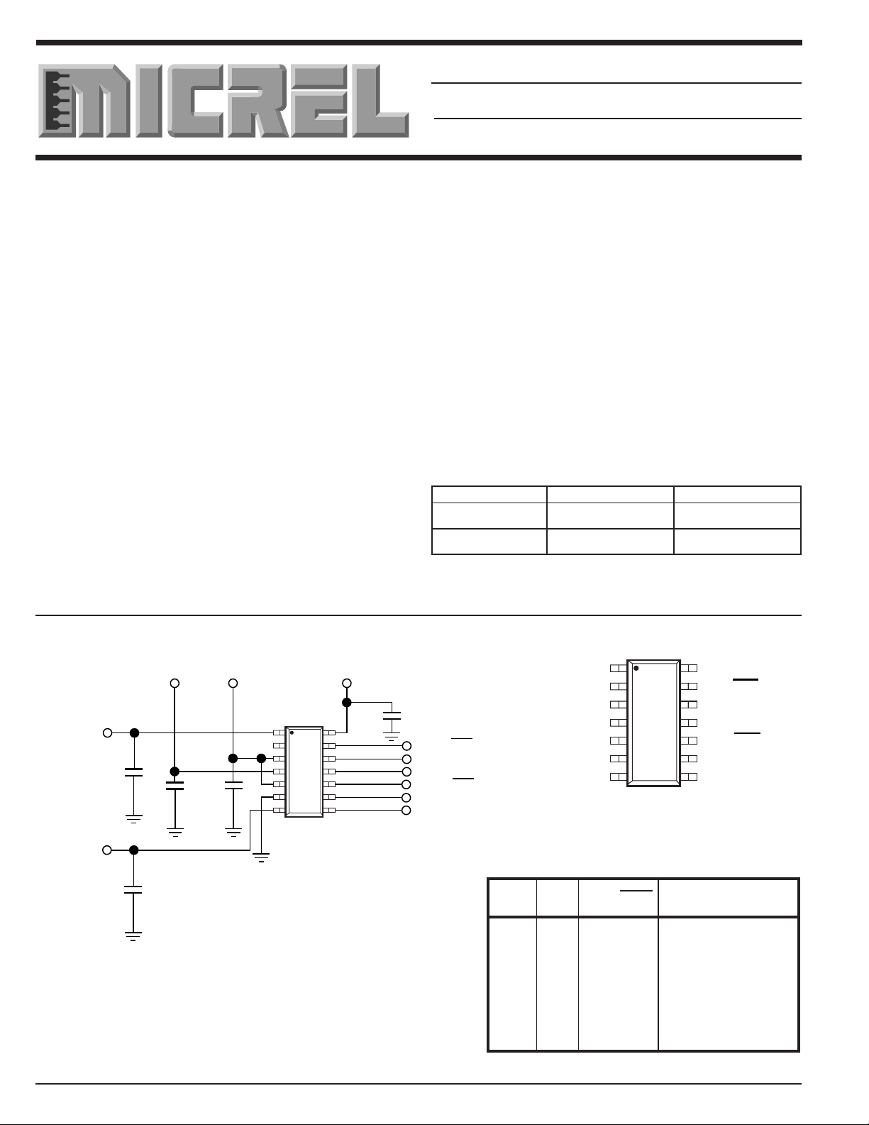
Typical Application
V
PP IN
+12V
V
PP OUT 1
V
PP OUT 2
0.1µF
0.1µF
1µF 1µF
V
CC
+3.3V or +5V
2
3
MIC2558
4
5
6
7
Pin Configuration
V
DD
+5V
0.1µF
14
13
12
11
10
9
8
Hi-Z/ Low 1 Control
EN0
1
EN1
1
Hi-Z/ Low 2 Control
EN0
2
EN1
2
V
V
PP
PP
OUT1
+V
CC1
V
PP
+V
CC2
GND
OUT2
NC
IN
2
3
MIC2558
4
5
6
7
EN1 EN0 Hi-Z/Low V
0 0 0 0V, (Sink current)
0 0 1 Hi-Z (No Connect)
01 x VCC (3.3V or 5.0V)
10 x V
1 1 x Hi-Z (No Connect)
14
13
12
11
10
9
8
PP OUT
PP
V
DD
Hi-Z/Low1
EN0
1
EN1
1
Hi-Z/Low2
EN0
2
EN1
2
2-10 1997
Page 2
MIC2558 Micrel
Absolute Maximum Ratings (Notes 1 and 2)
Power Dissipation, T
SOIC 800 mW
Derating Factors (To Ambient)
SOIC 4 mW/°C
Storage Temperature –65°C to +150°C
Operating Temperature (Die) 125°C
Operating Temperature (Ambient) –40°C to +85°C
Lead Temperature (5 sec) 260°C
AMBIENT
≤ 25°C
Supply Voltage, V
V
CC
V
DD
Logic Input Voltages –0.3V toV
Output Current (each Output)
V
PP OUT
V
PP OUT
PP IN
= 12V 600mA
= V
CC
15V
7.5V
7.5V
DD
250mA
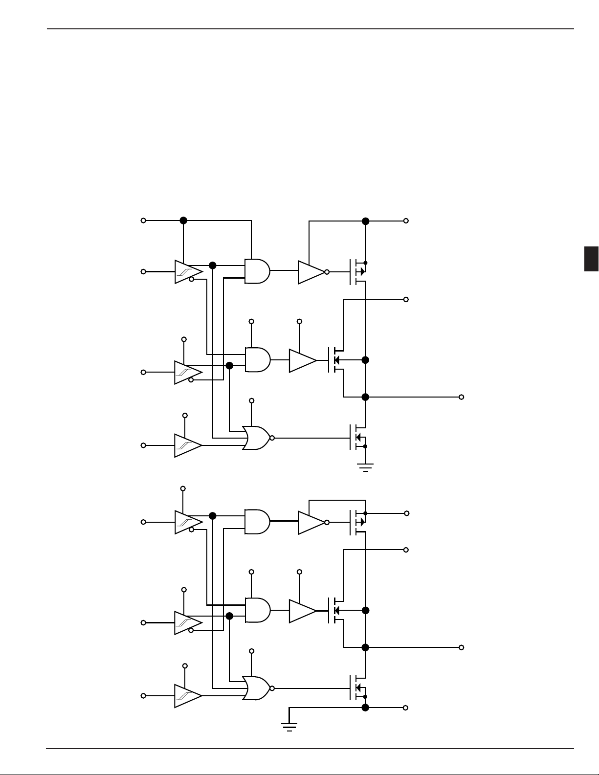
Logic Block Diagram
V
DD
EN1
EN0
HiZ/
LOW
V
14
PP IN
4
2
1
11
V
CC1
V
DD
V
DD
1
12
V
DD
13
1
V
DD
V
DD
V
PP IN
3
V
PP OUT1
1
EN1
2
8
V
PP IN
EN0
V
DD
V
DD
2
9
V
DD
V
DD
HiZ/
LOW
1997 2-11
10
2
5
6
V
PP IN
V
CC2
GND
7
V
PP OUT2
Page 3
MIC2558 Micrel
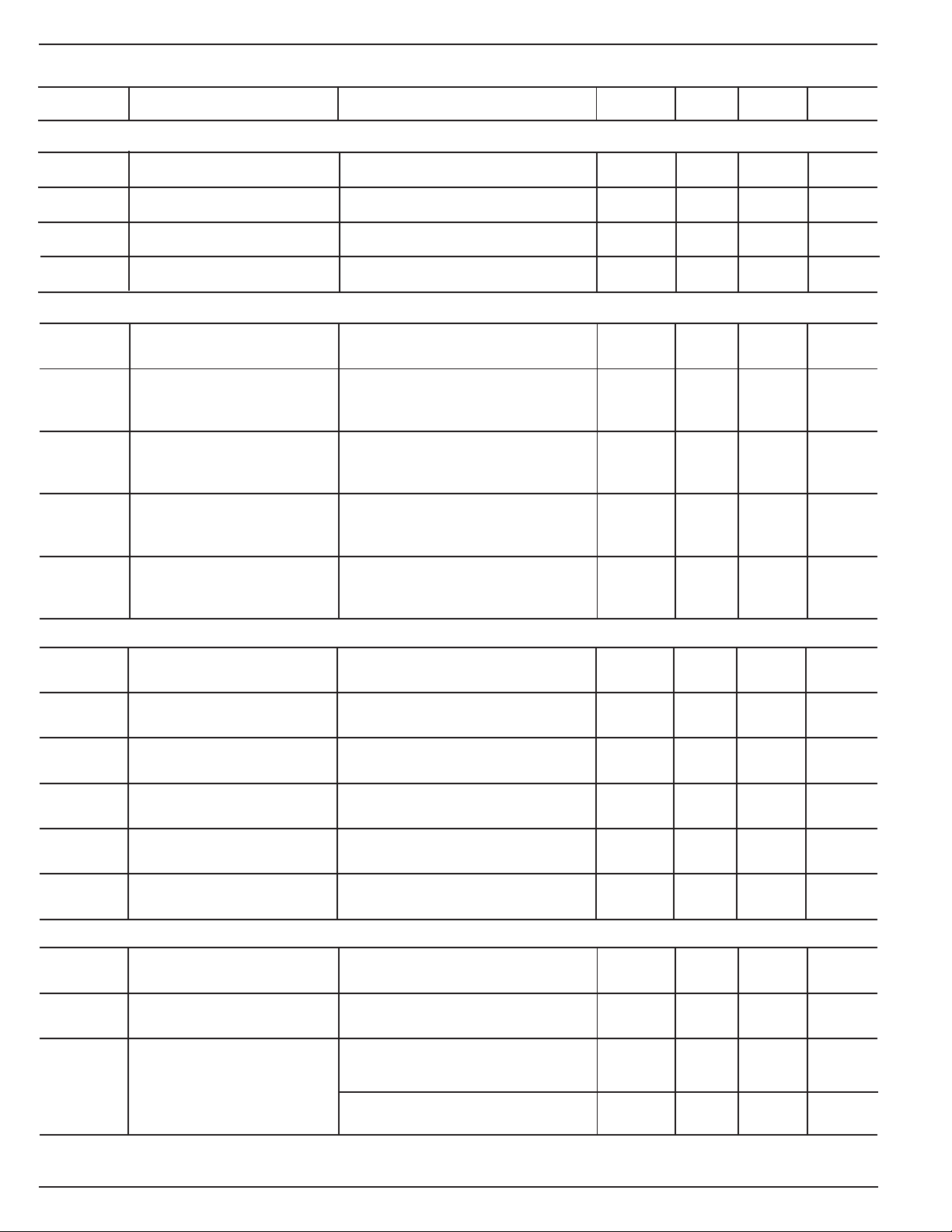
Electrical Characteristics:
(Over operating temperature range with V
DD
= VCC= 5V, V
= 12 V unless otherwise specified.)
PP IN
Symbol Parameter Conditions Min Typ Max Units
INPUT
V
IH
V
IL
VIN (Max) Input Voltage Range –5 V
I
IN
Logic 1 Input Voltage 2.2 V
Logic 0 Input Voltage 0.8 V
DD
Input Current 0 V < VIN < V
DD
±1 µA
EACH OUTPUT
V
OL
I
, Hi-Z High Impedance Output EN0 = EN1 = 0, HiZ = 1. 1 10 µA
OUT
R
OC
R
O
Clamp Low Output Voltage EN0 = EN1 = HiZ = 0, I
Leakage Current 0 ≤ V
PP OUT
≤ 12V
Clamp Low Output Resistance Resistance to Ground. I
EN0 = EN1 = 0, HiZ = 0.
Switch Resistance, I
V
PP OUT
= V
CC
PP OUT
= –10 mA (Sourcing) 2.5 5 Ω
= 1.6mA 0.4 V
SINK
= 2mA 130 250 Ω
SINK
V
R
O
Switch Resistance, I
V
PP OUT
= V
PP IN
SWITCHING TIME (See Figure 1)
t
1
t
2
t
3
t
4
t
5
t
6
Delay + Rise Time V
Delay + Rise Time V
Delay + Fall Time V
Delay + Fall Time V
Output Turn-On Delay V
Output Turn-Off Delay V
POWER SUPPLY
I
I
DD
CC
VDD Supply Current – 1 µA
VCC Supply Current I
PP OUT
PP OUT
PP OUT
PP OUT
PP OUT
PP OUT
PP OUT
PP OUT
= –100 mA (Sourcing) 0.5 1 Ω
= 0V to 5V (Notes 3, 5) 15 50 µs
= 5V to 12V (Notes 3, 5) 12 50 µs
= 12V to 5V (Notes 3, 5) 25 75 µs
= 5V to 0V (Notes 3, 5) 45 100 µs
= Hi-Z to 5V (Notes 4, 5) 10 50 µs
= 5V to Hi-Z (Notes 4, 5) 75 200 ns
= 0 – 1 µA
I
PP
IPP Supply Current V
PP OUT1
I
PPOUT
V
PP OUT1
= V
PPOUT2
= 0 V or VPP . – 10 µA
= 0.
= V
PPOUT2
= V
CC
20 80 µA
2-12 1997
Page 4
MIC2558 Micrel
Electrical Characteristics (continued)
Symbol Parameter Conditions Min Typ Max Units
POWER SUPPLY, continued
V
CC
VDDOperating Input Voltage 2.8 6 V
V
PP IN
NOTE 1: Functional operation above the absolute maximum stress ratings is not implied.
NOTE 2: Static-sensitive device. Store only in conductive containers. Handling personnel and equipment should be grounded to
NOTE 3: With RL = 2.9kΩ and C
NOTE 4: RL = 2.9kΩ. RL is connected to VCC during t5, and is connected to ground during t6.
NOTE 5: Rise and fall times are measured to 90% of the difference of initial and final values.
Operating Input Voltage 6V
Operating Input Voltage 8.0 14.5 V
prevent damage from static discharge.
= 0.1µF on V
OUT
PP OUT
.
3V
Hi-Z/Low
0
2
EN0
EN1
PP OUT
3V
0
3V
0
12V
5VV
0
t
1
t
2
t
3
t
4
t
5
t
6
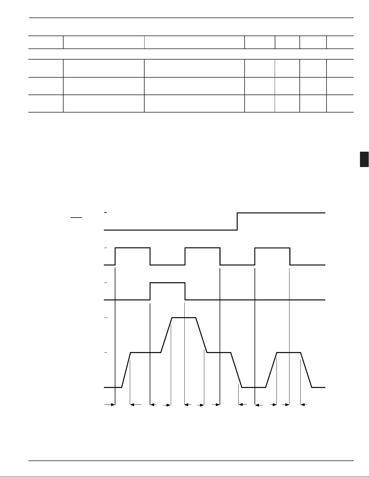
Figure 1. Timing Diagram.
1997 2-13
Page 5
MIC2558 Micrel
Applications Information
12V
5V
EN0
EN1
1
1
VCC Switch
V
PP IN
MIC2558
V
CC
V
CC
V
PP1
PCMCIA
Card Slot
A
PCMCIA V
using the MIC2558 voltage selector/switch IC. Two control
bits per V
PP
1
PP OUT
and V
control is easily accomplished
PP2
pin determine output voltage and standby/
operate mode condition. Output voltages of 0V (defined as
less than 0.4V), V
(3.3V or 5V), VPP, or a high impedance
CC
state, are available. When either the high impedance or low
voltage conditions are selected, the device switches into
"sleep" mode and draws only nanoamperes of leakage
current.
System
Power
Supply
The MIC2558 is a dual low-resistance power MOSFET
switching matrix that operates from the computer system
main power supply. Device power is obtained from VDD,
which may be either 3.3V or 5V, and FET drive is obtained
from V
(usually +12V). Internal break-before-make
PP IN
switches determine the output voltage and device mode.
V
PP1
and V
are completely indepenent from each other.
PP2
Supply Bypassing
For best results, bypass V
capacitors. Both V
PP OUT
CC
and V
inputs with 1µF
PP IN
pins should have a 0.01µF to
0.1µF capacitor for noise reduction and electrostatic discharge (ESD) damage prevention. Larger values of output
capacitor will create large current spikes during transitions,
requiring larger bypass capacitors on the V
System
Power
Supply
5V
3.3V
12V
EN0
EN1
V
CC
1
1
Select and
Switch
V
PP IN
MIC2558
and V
CC
V
CC
V
CC
V
PP1
PP IN
PCMCIA
Card Slot
pins.
A
EN0
PCMCIA
Card Slot
Controller
EN1
EN0
EN1
EN0
EN1
2
2
V
1
1
2
2
PP IN
MIC2558
V
CC
V
PP2
V
CC
V
PP1
PCMCIA
Card Slot
V
PP2
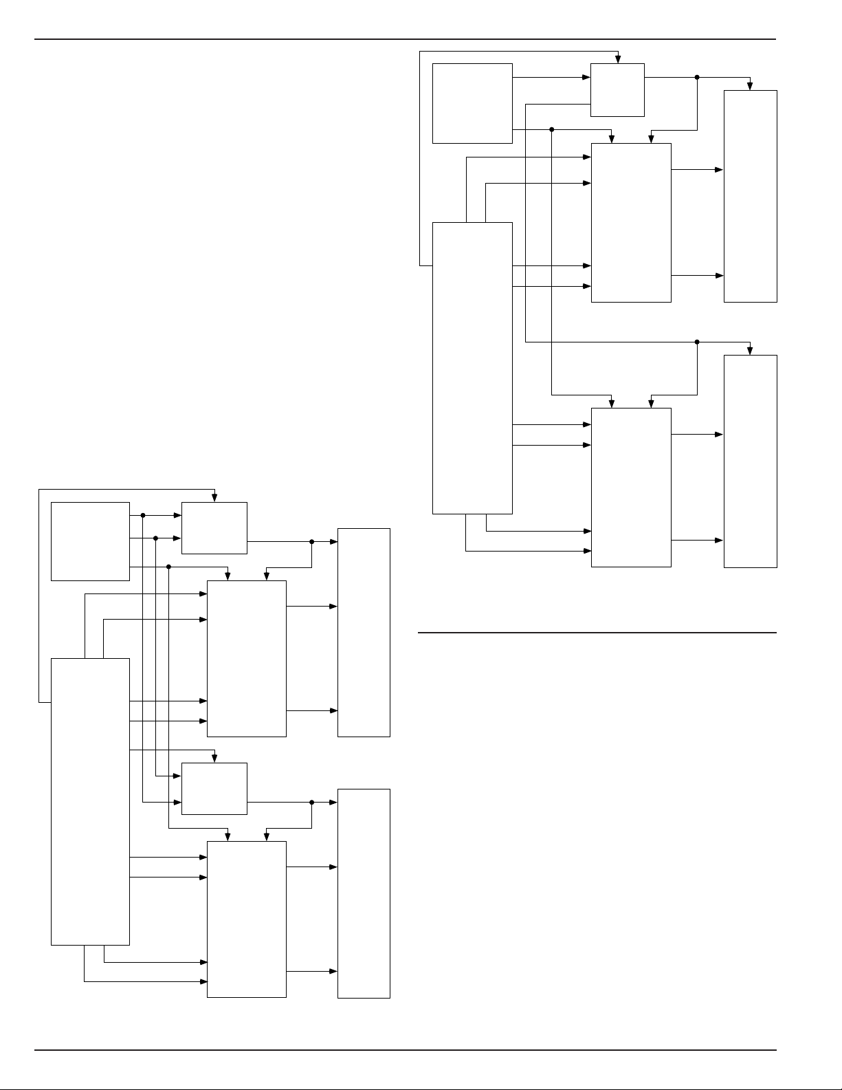
Figure 3. MIC2558 Typical two slot PCMCIA applica-
tion with single 5.0V VCC.
PCMCIA Implementation
B
EN0
PCMCIA
Card Slot
Controller
2
EN1
2
VCC Select and
Switch
EN0
1
V
PP IN
EN1
1
EN0
2
EN1
2
MIC2558
V
CC
V
PP2
V
CC
V
PP1
PCMCIA
Card Slot
B
V
PP2
Figure 2. MIC2558 Typical two slot PCMCIA applica-
tion with dual VCC (5.0V or 3.3V).
The Personal Computer Memory Card International Association (PCMCIA) specification requires two VPP supply pins
per PCMCIA slot. VPP is primarily used for programming
Flash (EEPROM) memory cards. The two VPP supply pins
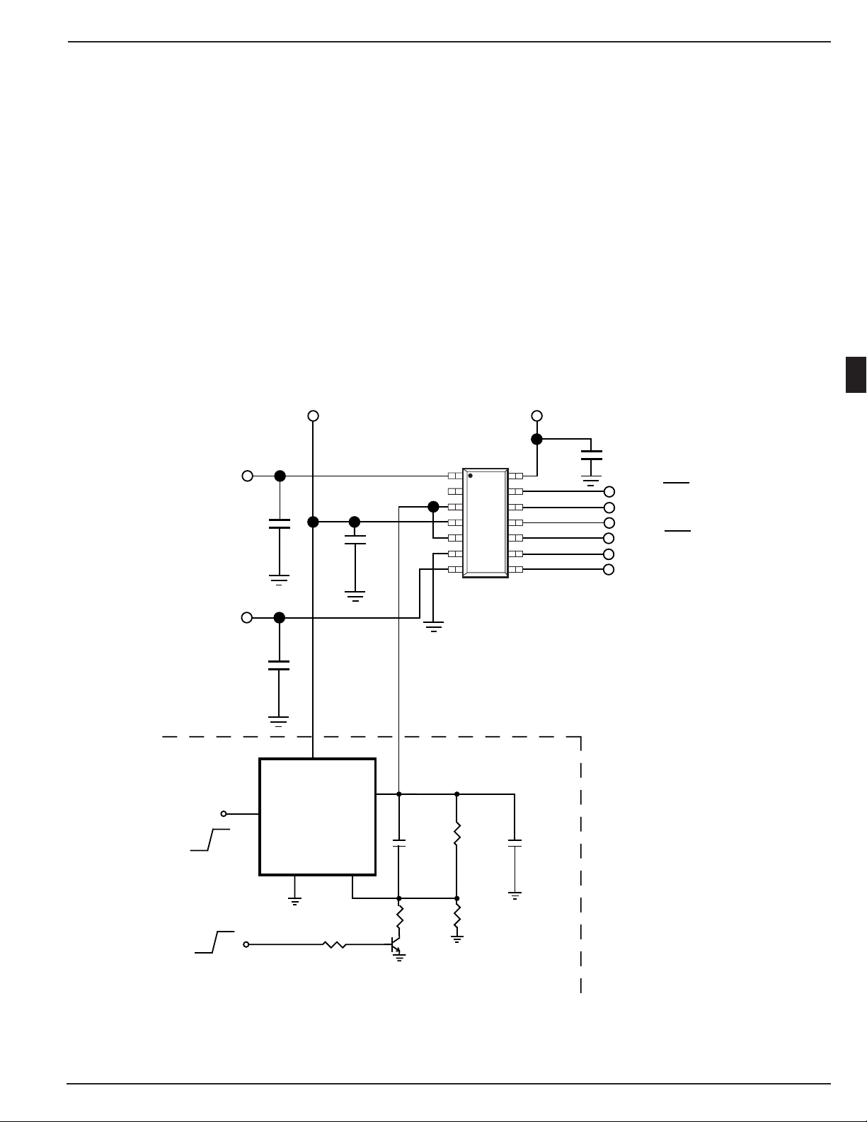
may be programmed to different voltages. Fully implementing PCMCIA specifications requires a MIC2558 and a controller. Figure 2 shows this full configuration, supporting both
5.0V and 3.3V VCC operation. Figure 3 is a simplified design
with fixed VCC = 5V.
When a memory card is initially inserted, it should receive
VCC — usually 5.0V ±5%. The card sends a handshaking
data stream to the controller, which then determines whether
or not this card requires VPP and if the card is designed for
5.0V or 3.3V VCC. If the card uses 3.3V VCC, the controller
commands this change, which is reflected on the VCC pins of
both the PCMCIA slot and the MIC2558.
During Flash memory programming, the PCMCIA controller
outputs a (1,0) to one or both halves of the MIC2558, which
connects V
PP IN
to V
PP OUT1
and/or V
PP OUT2
. The low ON
resistance of the MIC2558 switch requires only a small
bypass capacitor on the V
PP OUT
pins, with the main filtering
2-14 1997
Page 6
MIC2558 Micrel
action performed by a large filter capacitor on V
V
PP OUT
transition from VCC to 12.0V typically takes 25µS.
PP IN
. The
After programming is completed, the controller outputs a
(0,1) to the MIC2558, which then reduces V
PP OUT
to the
VCC level. Break-before-make switching action reduces
switching transients and lowers maximum current spikes
through the switch from the output capacitor.
If no card is inserted, or the system is in sleep mode, the
controller outputs either a (0,0) or a (1,1) to the MIC2558.
Either input places the switch into shutdown mode, where
current consumption drops even further.
The HiZ/Low input controls the optional logic low output
clamp. With HiZ/Low in the high state and EN0 = EN1 = 0,
V
PP OUT
Low in the low state and EN0 = EN1 = 0, V
enters a high impedance (open) state. With HiZ/
PP OUT
is clamped
to ground, providing a logic low signal. The clamp does not
require any DC bias current for operation.
V
PP IN
+12V
V
PP OUT 1
0.1µF
1µF
MOSFET drive and bias voltage is derived from V
PP IN
Internal device control logic is powered from VDD, which
should be connected to the same supply voltage as the
PCMCIA controller (normally either 3.3V or 5V).
Output Current
MIC2558 output switches are capable of far more current
than usually needed in PCMCIA applications. PCMCIA V
PP
output current is limited primarily by switch resistance voltage
drop (I x R) and the requirement that V
more than 5% below nominal. V
short circuits to ground if V
PP IN
PP OUT
or VCC are current limited by
PP OUT
cannot drop
will survive output
the regulator that supplies these voltages.
V
DD
+5V
0.1µF
14
2
3
MIC2558
4
5
6
7
13
12
11
10
9
8
Hi-Z/ Low 1 Control
EN0
1
EN1
1
Hi-Z/ Low 2 Control
EN0
2
EN1
2
.
2
V
PP OUT 2
0.1µF
SHUTDOWN
INPUT
ON
TTL Logic Level
High (V > 1.5V) VCC = 5.0V
Low (V < 0.5V) VCC = 3.3V
OFF
3
SD
GND
4
8
+V
IN
MIC2951
470 kΩ
V
7
OUT
FB
VIN = +5.3V to +15V
1
100pF
220kΩ
1%
2N2222
300kΩ
1%
180kΩ
1%
+
3.3µF
VCC Switching and Control Block
Figure 3. Full PCMCIA Implementation of VPP and VCC switching using MIC2558 and MIC2951 voltage regulator.
1997 2-15
 Loading...