

Page 1
MIC2755 Micrel
MIC2755
Battery System Supervisor
Preliminary Information
General Description
The MIC2755 is composed of multiple comparators, a reset
pulse generator, and logic. It is designed for monitoring the
battery supply of portable digital systems, including PDAs
and pagers.
The MIC2755 detects three different battery states: battery
OK, low battery, and dead battery. The reset (/RST) output is
asserted for at least 700ms when a fresh battery is inserted.
The nonmaskable interrupt output (/NMI) is asserted when
the battery voltage is below the NTH threshold, indicating that
high-power system operations should not occur. If and when
battery voltage falls below the power-off threshold (PTH), the
reset output is asserted and latched, inhibiting system operation until the battery is replaced or recharged.
All three voltage thresholds are set using external resistors.
A manual reset function can be implemented by connecting
a switch directly to the power on reset/manual reset [RTH(/MR)]
input. Internal circuitry detects switch activation and generates a minimum 175ms debounced reset signal. The
MIC2755’s power supply input is separate from the detector
inputs to allow it to be powered from a down-stream voltage,
such as the output of a boost converter.
Inputs and outputs can be pulled above V
absolute maximum) without adverse effects or excessive
current draw.
Supply current is typically a low 2µA. Hysteresis is included
on all voltage detectors to prevent chattering due to noise.
The MIC2755 is available in the tiny 8-lead micro-smalloutline package.
(up to 7V
DD
Features
• Optimized for PDAs, pagers and
other hand-held devices.
• Detects multiple battery states:
- battery OK
- low battery
- dead battery
• Adjustable voltage thresholds
• High accuracy ±2% voltage thresholds
• Reset generation at power-on (700ms min.)
• Debounced manual reset function
• Internal logic prevents chatter if battery voltage
fluctuates
• Extremely low 2µA typical supply current
• I/Os can be pulled above VDD (7V absolute maximum)
• Immune to brief power supply transients
• Low cost
• 8-lead MSOP
Applications
• PDAs
• Pagers
• Consumer electronics
• Embedded controllers
• Portable instruments
• Data loggers
Ordering Information
Part Number Junction Temp. Range Package
MIC2755BMM –40°C to +85°C 8-pin MSOP
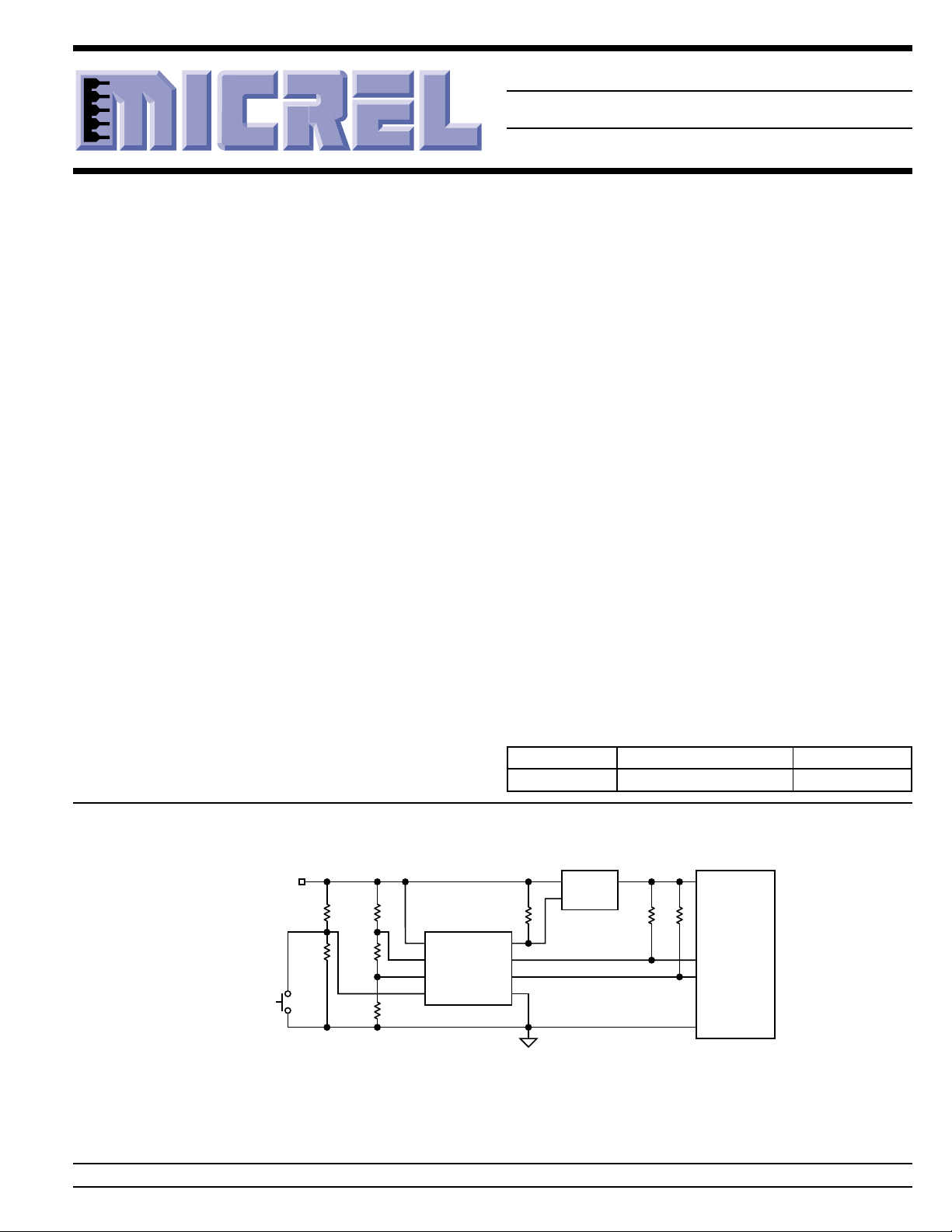
Typical Application
Boost or Buck
Converter
IN OUT
EN
V
BAT(OK)
V
BAT(low)
V
BAT(dead)
= 3.6V
= 3.1V
= 2.9V
SW
RESET
V
656k
344k
BAT
576k
26.7k
400k
MIC2755
VDD /POF
PTH
NTH
RTH(/MR)
/NMI
/RST
GND
100k 100k 100k
Supervised Boost Converter and Microcontroller or Microprocessor
Micrel, Inc. • 1849 Fortune Drive • San Jose, CA 95131 • USA • tel + 1 (408) 944-0800 • fax + 1 (408) 944-0970 • http://www.micrel.com
February 2000 1 MIC2755
µController or
µProcessor
SUPPLY
/NMI
/RST
GND
Page 2
MIC2755 Micrel
Pin Configuration
NTH
PTH
GND
Pin Description
Pin Number Pin Name Pin Function
1 RTH(/MR) Power-On Reset Threshold (Analog Input): Comparator input assigned to
2 NTH Nonmaskable Interrupt Threshold (Analog Input): Voltage monitor input
3 PTH Power-Off Threshold (Analog Input): Voltage monitor input assigned to
4 GND Ground: Power and signal return for all IC functions.
5 /POF Power-off (Output): Active-low, open-drain output. Asserted and latched
6 /NMI Nonmaskable Interrupt (Output): Active-low, open-drain output. Asserted
7 /RST Reset (Output): Active-low, open-drain output. Asserted for a minimum of
8 VDD (Analog Input): Power supply input.
1RTH(/MR)
2
3
4
8 VDD
/RST
7
/NMI
6
/POF
5
8-Lead MSOP (MM)
battery-OK condition detection. When the level on this pin first exceeds
, the reset generator cycles. The /RST output is held low for a minimum
V
REF
of 700ms and the /POF threshold output is deasserted.
assigned to “low battery” condition detection. When the level on this pin falls
below V
“dead battery” condition detection. When the level on this pin falls below
V
REF
a reset cycle occurs (V
when V
in reset until the battery is replaced and a power-on reset cycle occurs.
when V
power system operation should not be allowed.
700ms at power-on or anytime V
175ms minimum when RTH (/MR) is externally pulled low (manual reset).
, the /NMI output is asserted.
REF
, the /RST and /POF outputs are asserted. The condition is latched until
PTH
NTH
< V
< V
> V
RTH
, which is a “dead battery” condition. The system is held
REF
, which is a “low battery” condition. This indicates high-
REF
).
REF
drops below V
PTH
. Also asserted for
REF
MIC2755 2 February 2000
Page 3

MIC2755 Micrel
Absolute Maximum Ratings (Note 1)
Supply Voltage (V
Input Voltage (V
Output Voltage (V
/RST Output Current (I
Storage Temperature (T
ESD Rating, Note 3 ......................................................2kV
) ..................................... –0.3V to +7V
DD
RTH
/RST
), (V
), (V
NTH
), (V
/NMI
) .......................................20mA
/RST
) ....................... –65°C to +150°C
S
) ............. –0.3V to +7V
PTH
), (V
) ........ –0.3V to +7V
/POF
Operating Ratings (Note 2)
Supply Voltage (V
Input Voltage (V
Output Voltage (V
Ambient Temperature Range (TA) ............. –40°C to +85°C
Package Thermal Resistance
1-layer PCB (θ
) .................................. +1.5V to +5.5V
DD
), (V
RTH
/RST
) ..............................................206°C/W
JA
NTH
), (V
), (V
/NMI
) ............. –0.3V to +6V
PTH
), (V
) ........ –0.3V to +6V
/POF
4-layer PCB (θJA) ..............................................113°C/W
Electrical Characteristics
VDD = 3.3V; TA = 25°C, bold values indicate –40°C ≤ TA ≤ +85°C; unless noted
Symbol Parameter Condition Min Typ Max Units
I
DD
I
RTH(/MR)
, I
I
NTH
PTH
I
/RST, I/NMI
I
/POF
V
REF1
V
REF2
V
HYST
Reset Output (/RST)
t
/RST
t
/MR
V
/RST
Reset Input [RTH(/MR)]
V
/MRTV
t
DBNC
t
PROP
Nonmaskable Interrupt Output (/NMI)
t
PROP
V
/NMI
Power-Off Output (/POF)
t
PROP
V
/POF
Note 1. Exceeding the absolute maximum rating may damage the device.
Note 2. The device is not guaranteed to function outside its operating rating.
Note 3. Devices are ESD sensitive. Handling precautions recommended. Human body model, 100pF in series with 1.5k .
Note 4. VDD operating range is 1.5V to 5.5V. Output is guaranteed to be held low down to VDD = 1.2V.
Note 5.
Operating Supply Current outputs open, V
outputs open, V
RTH
RTH
, V
, V
NTH
NTH
, V
> 1.24V 2.0 4.0 µA
PTH
, V
< 1.24V 1.7 µA
PTH
, Leakage Current 5pA
, 10 nA
,
Threshold Voltage for RTH(/MR) and PTH inputs 1.215 1.240 1.265 V
Threshold Voltage for NTH inputs 1.215 1.240 1.265 V
Hysteresis Voltage on NTH 20 mV
Comparator
Reset Pulse Width 700 1200 ms
Manual Reset Pulse Width 175 300 ms
/RST Output Voltage Low, Note 4 /RST asserted, I
/RST asserted, I
= 1.6mA, VDD ≥ 1.6V 0.3 V
SINK
= 100µA, VDD ≥ 1.2V 0.4 V
SINK
Manual Reset Trip Voltage 275 310 345 mV
Debounce Time V
/MRTV(min)
Propogation Delay from (V
to RST Asserted
Propagation Delay (V
REF(max)
< V
RTH
< V
/MR
RTH(/MR)(min)
+ 100mV) < V
< V
/MRTV(max)
, Note 5 22 38 ms
– 100mV) 9 µs
NTH
< (V
REF(min)
9 µs
– 100mV)
/NMI Output Voltage Low /NMI asserted, I
/NMI asserted, I
Propagation Delay (V
– 100mV)
/POF Output Voltage Low /POF asserted, I
/POF asserted, I
t
t
t
DBNC
/RST /MR
==
32
8
. These relationships are guaranteed by design.
REF(max)
+ 100mV) < V
= 1.6mA, VDD ≥ 1.6V 0.3 V
SINK
= 100µA, VDD ≥ 1.2V 0.4 V
SINK
< (V
PTH
= 1.6mA, VDD ≥ 1.6V 0.3 V
SINK
= 100µA, VDD ≥ 1.2V 0.4 V
SINK
REF(min)
9 µs
February 2000 3 MIC2755
Page 4
MIC2755 Micrel
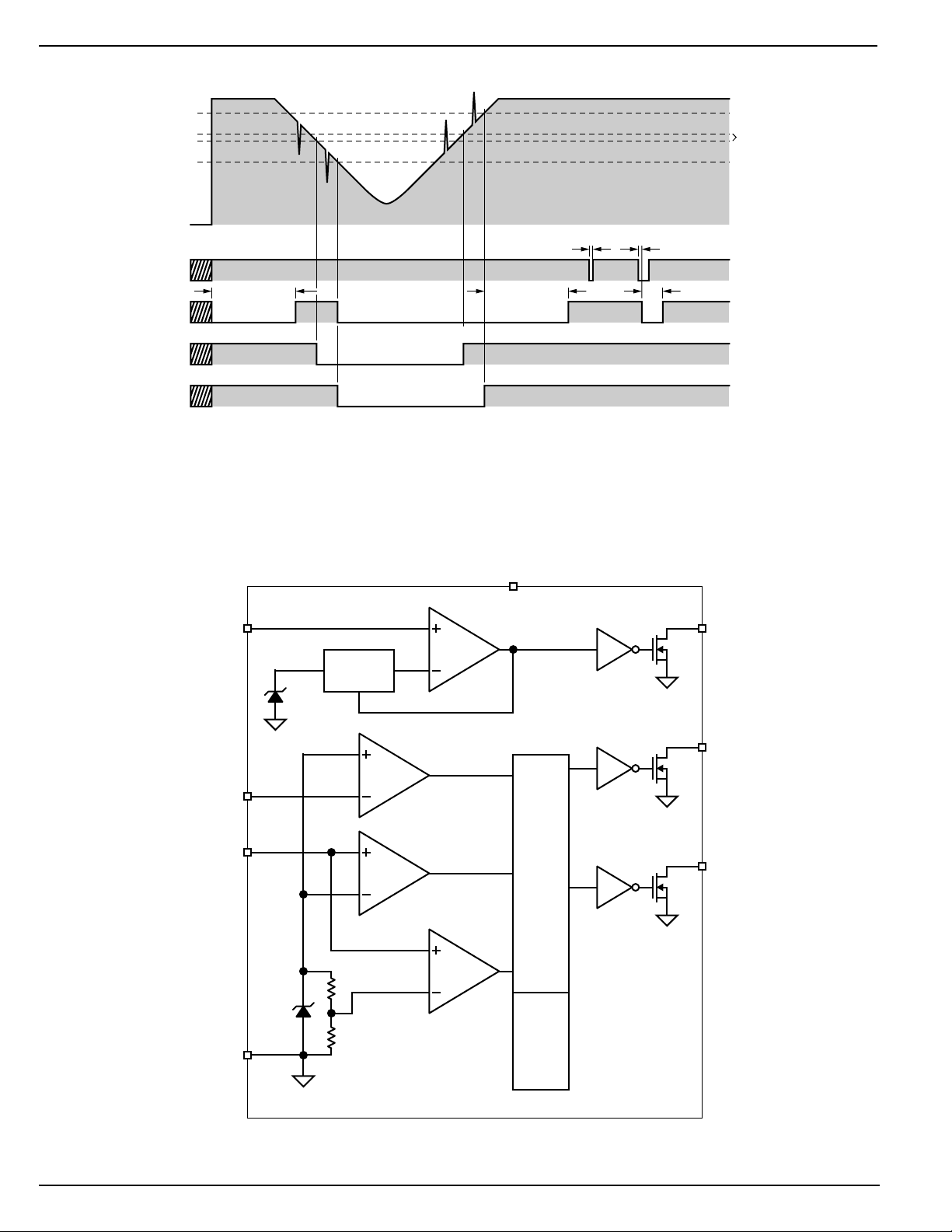
Timing Diagram
V
V
V
BAT
V
V
/MR
/RST
/NMI
/POF
V
V
V
V
V
V
V
/MRH
/MRL
/RSTH
/RSTL
/NMIH
/NMIL
/POFH
/POFL
V
V
V
V
Block Diagram
PTH
0V
RTH
NTH
t
RST
Propagation delays not shown for clarity.
The MIC2755 ignores very brief transients. See “Application
Information” for details.
t
RST
<t
DBNC
>t
DBNC
t
/MR
NOT TO SCALE.
20mV
V
EXPANDED
BAT
VERTICALLY TO
SHOW DETAIL.
NTH
PTH
RTH(/MR)
1.24V
Ref1
1.24V
Ref2
20mV
Hysteresis
310mV
VDD
Machine
Logic-State
/NMI
/RST
/POF
GND
Oscillator
MIC2755 4 February 2000
Page 5

MIC2755 Micrel
Functional Description
Typically the MIC2755 is used to monitor the battery supply
of intelligent circuits such as microcontrollers and microprocessors. By connecting the reset output of a MIC2755 to the
reset input of a µC or µP, the processor will be properly reset
at power-on and during power-down and low battery conditions. The /NMI output provides low-battery warnings to the
system. In addition, a system whose battery voltage declines
below the PTH threshold is held in reset to prevent spurious
operation. Thus the MIC2755 effectively detects three battery
states: “battery OK,” “low battery,” and “dead battery.”
Reset Output
/RST is an active-low, open-drain digital output. This output
is asserted for a minimum of 700ms at power-on and for a
minimum of 175ms when RTH(/MR) is externally pulled low,
indicating that a manual reset should be initiated. /RST is an
active-low, open-drain digital output and may be wire-ORed
with other open-drain logic signals. Most applications will
require a pull-up resistor on this pin. /RST may be pulled up
to any voltage not exceeding V
/RST(max)
higher than VDD (see “Electrical Characteristics”).
Nonmaskable Interrupt Output
/NMI is the output of a comparator that constantly compares
the level on the NTH pin with the internal voltage reference,
V
. This output is asserted when V
REF2
high-power system operation should not occur; that is, the
battery is low but not dead. Effectively, this function is an
uncommitted comparator with its inverting input connected to
the internal reference, V
, its noninverting input con-
REF2
nected to NTH, and its output on /NMI. This comparator does
not affect any other MIC2755 functions and may be used
independently.
/NMI is an active-low, open-drain digital output and may be
wire-ORed with other open-drain logic signals. Most applications will require a pull-up resistor on this pin. /NMI may be
pulled up to any voltage not exceeding V
voltage is higher than VDD (see “Electrical Characteristics”).
even if this voltage is
< V
NTH
/NMI(max)
, indicating
REF2
even if this
Power-Off Output
This output and the /RST output are asserted and latched
when V
PTH
< V
, indicating a “dead battery.” The system
REF
is held in reset until the battery is replaced or recharged and
a power-on reset cycle occurs; that is, V
RTH
> V
REF1
. The
/POF output may be used to control a linear or switching
regulator, shutting down the regulator when the battery
reaches it end-of-life voltage.
/POF is an active-low, open-drain digital output and may be
wire-ORed with other open-drain logic signals. Most applications will require a pull-up resistor on this output. /POF may
be pulled up to any voltage not exceeding V
/POF(max)
even if
this voltage is higher than VDD (see “Electrical Characteristics”).
Power-On Reset
The RTH(/MR) and PTH inputs work together to provide
predictable battery monitoring with user-programmable hysteresis and without chatter. The /RST output is asserted for
a minimum of 700ms at power-on. Power-on is determined by
RTH(/MR) exceeding V
. Once this event has occurred,
REF1
the internal logic ignores further transitions on the RTH(/MR)
input, instead monitoring for a low voltage on PTH or the
manual reset condition. If V
drops below V
PTH
REF1
, the /POF
and /RST outputs are asserted and latched, holding the
system in its reset state.
Manual Reset
An internal circuit monitors RTH(/MR), comparing it to an
internal 310mV reference, V
below V
/MRTV,
and V
is still above V
PTH
. When RTH(/MR) is pulled
/MRTV
REF1
, the internal
circuitry initiates a manual reset cycle and asserts /RST for at
least 175ms. A momentary push-button switch is typically
connected such that RTH(/MR) is forced to ground when the
switch contacts close. This switch is internally debounced.
Each closure of the switch longer than t
results in a
DBNC
single output pulse of no less than 175ms and no more than
300ms being generated. (The manual reset pulse is derived
from the same oscillator and counter as t
t
is always equal to one fourth of t
/MR
/RST
. The length of
/RST
.) This prevents a
user who may hold the switch closed from keeping the system
in reset for an extended period of time.
February 2000 5 MIC2755
Page 6

MIC2755 Micrel
V=V
R6 R7
R7
BAT(OK)
REF
+
Applications Information
Outputs
Since the MIC2755 outputs are open-drain MOSFETs, most
applications will require pull-up resistors. The value of the
resistors should not be too large or leakage effects may
dominate.
Programming Thresholds
There are separate resistive-divider configurations for circuits that require or do not require manual reset capability.
Configuration Without Manual Reset
See Figure 1. The battery-OK threshold is calculated using:
R1 R2 R3 R4
VV
BAT(OK)
=
REF
4
R
+++
The low-battery threshold is calculated using:
R1 R2 R3 R4
+++
VV
BAT(low) REF
=
R3 R4
+
The dead-battery threshold is calculated using:
R1 R2 R3 R4
+++
VV
BAT(dead) REF
=
R2 R3 R4
++
where, for all equations:
V
= 1.24V
REF
In order to provide the additional criteria needed to solve for
the resistor values, the resistors can be selected such that
they have a given total value, that is, R1 + R2 + R3 + R4 =
R
. A value such as 1MΩ for R
total
total
because it draws minimum battery current per resistor ladder
but has no significant effect on system accuracy.
When working with large resistors, a small amount of leakage
current can cause voltage offsets that degrade system accuracy. The maximum recommended total resistance from
V
to ground is 3MΩ.
BAT
V
BAT
R1
572k
R2
28k
R3
55.6k
R4
344k
MIC2755
VDD /POF
PTH
NTH
RTH(/MR)
/NMI
/RST
GND
Figure 1. Example Circuit without Manual Reset
Once the desired trip points are determined, set the V
threshold first.
For a typical single-cell lithium ion battery, 3.6V is a reasonable “OK threshold” because at 3.6V the battery is moderately charged. Solving for R4:
1M
V 3.6V 1.24V
BAT(OK)
==
Ω
R
4
is a reasonable value
V
BAT
100k 100k100k
POF
NMI
RST
BAT(OK)
To determine the resistor values for V
BAT(low)
threshold, set
R4 = 344kΩ and solve for R3.
V = 3.1V=1.24V
BAT(low)
R+R4
3
1M
Ω
R3 = 56k
Once R3 and R4 are determined, the equation for V
BAT(dead)
can be used to determine R2. A single lithium-ion cell should
not be discharged below 2.5V. Many applications limit the
drain to 2.9V. Using 2.9V for the V
BAT(dead)
threshold allows
calculating the following resistor values.
1M
V = 2.9V=1.24V
BAT(dead)
R2+ 55.6k+ 344k
Ω
R2 = 27.4k
R1 = 1MΩ – R2 – R3 – R4 = 572k
Configuration With Manual Reset
See Figure 2. To use manual reset, the MIC2755 requires a
separate resistor ladder for the switch and fresh-battery
threshold. The remaining two thresholds are set by the threeresistor ladder.
SW
V
BAT
656k
344k
R6
R7
R8
573k
R9
26.7k
R10
400k
MIC2755
VDD /POF
PTH
NTH
RTH(/MR)
/NMI
/RST
GND
100k 100k100k
V
BAT
POF
NMI
RST
Figure 2. Example Circuit with Manual Reset
R8+R9+R10
V=V
BAT(low) REF
V=V
BAT(dead) REF
R8+R9+R10
R10
R9+R10
where, for all equations:
V
= 1.24V
REF
Once the desired trip points are determined, set R6 + R7 =
1MΩ and solve for R7.
1M
Ω
V = 3.6V=1.24V
BAT(fresh)
R7
R7 = 344k
R6 = 1MΩ – 344k = 656k
The remaining resistor values are solved in a similar manner
as the above.
1MΩ = R8 + R9 + R10
R4 = 344kΩ
MIC2755 6 February 2000
Page 7

MIC2755 Micrel
1M
Ω
V = 3.1V=1.24V
BAT(low)
R10
R10 = 400k
1MΩ = R10+R11
V = 2.9V=1.24V
BAT(dead)
R9+ 400k
1M
Ω
R9 = 27k
R8 = 1MΩ – R9 – R10 = 573k
The accuracy of the resistors can be chosen based upon the
accuracy required by the system.
Input Transients
The MIC2755 is inherently immune to very short negativegoing “glitches.” Very brief transients may cross the V
or V
BAT(dead)
thresholds without tripping the output(s).
BAT(lo)
As shown in Figures 3 and 4, the narrower the transient, the
deeper the threshold overdrive that will be ignored by the
MIC2755. The graph represents the typical allowable transient duration for a given amount of threshold overdrive that
will not cause the corresponding output to change state.
Alternate Configurations
The MIC2755 can be used in a variety of ways. It is especially
flexible due to the fact that the NMI comparator is completely
independent. There are other useful configuration besides a
three-state battery monitor. The NMI comparator can be used
to provide power-fail indication (PFI/PFI), monitor an auxiliary
battery (LBI/LBO), or detect the presence of an ac adapter.
Voltage Supervisor and Backup Battery Monitor
Figure 5 illustrates the MIC2755 being used as a voltage
supervisor and a battery monitor in a 3.3V system with a
Lithium coin-cell backup. The primary voltage monitor is
configured as a voltage supervisor with a nominal trip point of
3.034V and 33mV of hysteresis as set by R1, R2, and R3. The
NMI comparator is used to detect a low-battery condition so
the system is aware that the backup battery is discharged. In
this example, the /NMI output will be asserted if battery
voltage falls below 2.2V. Manual reset capability can be
added as discussed in the
With Manual Reset
sections.
Manual Reset
and
Configuration
This same configuration can be used to detect the presence
of an auxiliary power source such as an ac adapter instead of
monitoring a battery. R4 and R5 would be selected such that
the /NMI output is deasserted when the proper input voltage
is applied.
Voltage Supervisor with Power Fail Warning
Figure 6 illustrates the MIC2755 being used as a voltage
supervisor and a power-fail detector in a 3.3V system. The
primary voltage monitor is configured as a voltage supervisor
Input Transient
200
180
160
140
120
100
MAX. TRANSIENT DURATION (µs)
RESET COMP. OVERDRIVE, V
Response (V
80
60
40
20
0
0 5 10 15 20 25 30
POF
REF–VPTH
)
(mV)
Figure 3. Input Transient Response
Input Transient
120
100
MAX. TRANSIENT DURATION (µs)
RESET COMP. OVERDRIVE, V
Response (V
80
60
40
20
0
0 5 10 15 20 25 30 35 40 45
)
NMI
REF–VNTH
(mV)
Figure 4. Input Transient Response
with a nominal trip point of 3.034V and 33mV of hysteresis as
set by R1, R2, and R3. The NMI comparator is used to detect
an impending power failure such as a low-battery condition or
ac power outage. The /NMI output will be asserted if the input
voltage to the LDO regulator falls below 3.55V. (The MIC5245
has a specified maximum dropout of 250mV at 150mA output
current. If the input voltage falls below 3.55V, the output may
droop.)
By monitoring the input of the LDO regulator, the system
receives the earliest warning of an impending power loss.
Manual reset capability can be added as discussed in the
Manual Reset
and
Configuration With Manual Reset
sec-
tions.
Supervised Boost Converter and Microcontroller or
Microprocessor
In Figures 7 and 8, the MIC2755 is used to monitor the battery
and the MIC3172 is used to maintain the output voltage at
3.3V by boosting the input voltage. When the Li-ion battery
voltage drops to 3.1V, the MIC2755 alerts the microcontroller
or the microprocessor. When the battery voltage drops to
2.9V, the MIC2755 turns off the MIC3172.
February 2000 7 MIC2755
Page 8

MIC2755 8 February 2000
MIC2755
PTH
RTH(/MR)
NTH
VDD /POF
/RST
/NMI
3.3V
Power Rail
Power Fail
Warning Flag
System
Reset
GND
V
MAIN
R4
436k
R5
564k
R1
1.77M
R2
13.2k
R3
1.21M
R
PULLUP
R
PULLUP
R
PULLUP
MIC5205-3.3
EN
IN OUT
GND
Backup
Power
Lithium
Coin
Cell
MIC2755
PTH
RTH(/MR)
NTH
VDD /POF
/RST
/NMI
3.3V
Power Rail
Power Fail
Warning Flag
System
Reset
GND
V
BAT
R4
651k
R5
349k
R1
1.77M
R2
13.2k
R3
1.21M
R
PULLUP
R
PULLUP
R
PULLUP
MIC5245-3.3
EN
IN OUT
GND
MIC2755 Micrel
Figure 5. Voltage Supervisor and Backup Battery Monitor
Figure 6. Voltage Supervisor With Power Fail Warning
Page 9

February 2000 9 MIC2755
PGND1
MIC3172
MIC2755
SGND
COMP
EN
IN
PTH
RTH(/MR)
NTH
VDD
µController or
µProcessor
RST
GND
NMI
SUPPLY
/POF
8
1
2
3
5
6
7
4
/RST
/NMI
GND
FB
L1b
33µH
C7 10µF 16V
L1a
33µH
SW
PGND2
C5
0.01µF
R7
4.75k
R6
100k
V
BAT(OK)
= 3.6V
V
BAT(low)
= 3.1V
V
BAT(dead)
= 2.9V
R1
569k
R2
28k
C6
3300pF
C1
10µF
16V
R3
55.6k
R4
344k
Li-Ion
Cell
R10
3.01k
R11
1.82k
C3
220µF
10V
C2
220µF
10V
C4
0.1µF
R8
100k
3.3V @ 200mA
R9
100k
PGND1
MIC3172
MIC2755
SGND
COMP
EN
IN
PTH
RTH(/MR)
NTH
VDD
µController or
µProcessor
RST
GND
NMI
SUPPLY
/POF
8
1
2
3
5
6
7
4
/RST
/NMI
GND
FB
L1b
33µH
C2 10µF 16V
L1a
33µH
SW
PGND2
C5
0.01µF
R8
4.75k
R7
100k
C6
3300pF
C1
10µF
16V
R4
656k
R5
344k
Li-Ion
Cell
R1
576k
SW
R2
26.7k
R3
400k
R11
3.01k
R12
1.82k
C4
220µF
10V
C3
220µF
10V
C5
0.1µF
R9
100k
R10
100k
V
BAT(OK)
= 3.6V
V
BAT(low)
= 3.1V
V
BAT(dead)
= 2.9V
3.3V @ 200mA
MIC2755 Micrel
Figure 7. Typical Application Without Manual Reset
Figure 8. Typical Application With Manual Reset
Page 10

MIC2755 Micrel
Package Information
0.122 (3.10)
0.112 (2.84)
0.036 (0.90)
0.032 (0.81)
0.012 (0.03)
0.0256 (0.65) TYP
0.199 (5.05)
0.187 (4.74)
0.120 (3.05)
0.116 (2.95)
0.043 (1.09)
0.038 (0.97)
0.012 (0.30) R
0.008 (0.20)
0.004 (0.10)
8-Lead MSOP (MM)
5° MAX
0° MIN
DIMENSIONS:
INCH (MM)
0.007 (0.18)
0.005 (0.13)
0.012 (0.03) R
0.039 (0.99)
0.035 (0.89)
0.021 (0.53)
MIC2755 10 February 2000
Page 11

MIC2755 Micrel
February 2000 11 MIC2755
Page 12

MIC2755 Micrel
MICREL INC. 1849 FORTUNE DRIVE SAN JOSE, CA 95131 USA
TEL + 1 (408) 944-0800 FAX + 1 (408) 944-0970 WEB http://www.micrel.com
This information is believed to be accurate and reliable, however no responsibility is assumed by Micrel for its use nor for any infringement of patents or
other rights of third parties resulting from its use. No license is granted by implication or otherwise under any patent or patent right of Micrel Inc.
© 2000 Micrel Incorporated
MIC2755 12 February 2000
 Loading...