

Datasheet MIC2754-TBM5UET, MIC2753-TBM5UDT, MIC2754-LBM5UEL, MIC2754-MBM5UEM, MIC2754-RBM5UER Datasheet (MICREL)
...Page 1
June 1999 1 MIC2753/2754
MIC2753/2754 Micrel
MIC2753/2754
Power Supply Supervisors
Preliminary Information
General Description
The MIC2753 and MIC2754 are ultraminiature, full-featured,
power supply supervisors featuring active-high and activelow reset outputs, respectively.
The MIC2753/4 includes an undervoltage detector with a
power-on reset generator and reset output, an overvoltage
detector with a separate output for activating crowbar circuits,
and a debounced manual reset input. Typical supply current
is a low 30µA.
These devices provide a 140ms minimum reset output at
power-on and assert their reset outputs any time the input
voltage deviates beyond preset overvoltage or undervoltage
thresholds. Reset outputs remain asserted for 140ms (minimum) after the input returns to normal or after releasing the
manual reset. When an overvoltage condition is detected, the
overvoltage output is immediately activated. Hysteresis on
both thresholds prevents erratic operation due to noise.
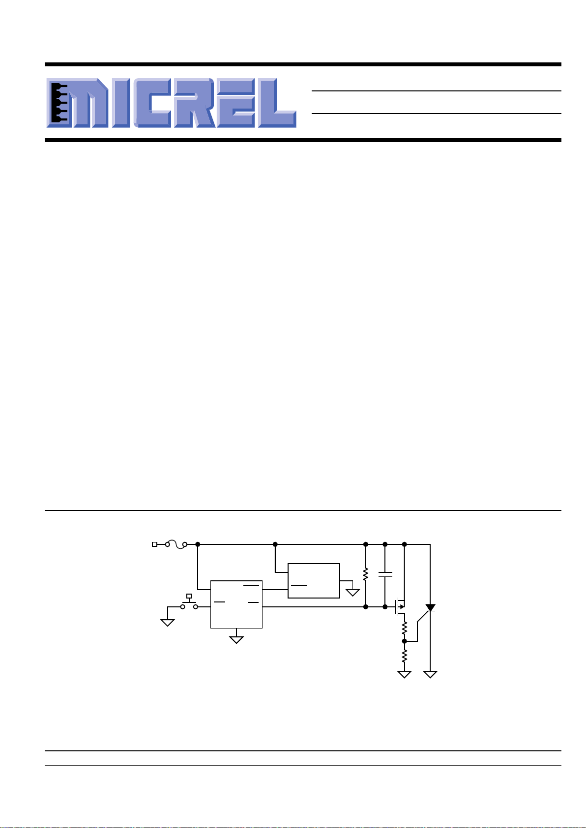
Typical Application
Microcontroller
Manual
Reset
MIC2754
VCC
HVMR
RST
V
CC
VIN
RST IN
GND
GND
Fuse
SCR
Crowbar
Micrel, Inc. • 1849 Fortune Drive • San Jose, CA 95131 • USA • tel + 1 (408) 944-0800 • fax + 1 (408) 944-0970 • http://www.micrel.com
Features
• Undervoltage and overvoltage monitor
• Separate overvoltage flag output
• Generates 140ms (minimum) power-on reset pulse
• Debounced manual reset input
• Choice of active-high (MIC2753) or
active-low (MIC2754) reset outputs
• Low 30µA typical supply current
• No external components needed
• IttyBitty™ SOT-23-5 package
Applications
• Computer systems
• Embedded controllers
• Power supplies
• Telecommunications systems
Page 2
MIC2753/2754 Micrel
MIC2753/2754 2 June 1999
Pin Configuration
Part
Identification
RST
MRGND
VIN
UDx
13
45
2
HV HV
MRRST
VIN
UEx
13
45
2
GND
MIC2753
MIC2754
Voltage
Code
Pin Description
Pin No. Pin No. Pin Name Pin Function
MIC2753 MIC2754
1 RST Reset (Digital Output): Active-high output. Asserted when V
IN
falls below
V
THU
(undervoltage threshold), or rises above V
THO
(overvoltage threshold).
Deasserted no less than 140ms after VIN returns within threshold limits.
2 1 /HV High-Voltage Flag (Open-Drain Output): /HV is asserted (active low) when
the input voltage exceeds the V
THO
(overvoltage threshold). It indicates
power supply overvoltage and is intended for connection to a protection
device such as a “crowbar” circuit.
3 3 VIN Analog Input: Voltage monitor input and power supply input to the IC.
4 /RST Reset (Digital Output): Active-low digital output. This output will be asserted
whenever V
IN
falls below V
THU
(undervoltage threshold), or rises above
V
THO
(overvoltage threshold). It will be deasserted no less than 140ms after
VIN returns within the threshold limits.
4 2 GND Ground: Ground return for all IC functions.
5 5 /MR Manual Reset (Digital Input): Logic low initiates immediate, unconditional
reset. If VIN is within tolerance thresholds, when /MR is released (returns
high), the reset output(s) will be deasserted no less than 140ms later. /MR
may be driven by a CMOS or TTL logic signal or a mechanical switch.
(Switch debouncing is performed internally.) /MR has an internal pull-up to
VIN and may remain open if unused.
Ordering Information
Part Number Mark Lower Threshold Monitored Upper Threshold Reset Temperature Package
Voltage Voltage* Voltage Range
MIC2753-RBM5 UDR 2.63V 2.85V±5% 3.08V Active High –40°C to +85°C SOT-23-5
MIC2753-SBM5 UDS 2.93V 3.3V±10% 3.83V Active High –40°C to +85°C SOT-23-5
MIC2753-TBM5 UDT 3.08V 3.3V±5% 3.53V Active High –40°C to +85°C SOT-23-5
MIC2753-MBM5 UDM 4.38V 5.0V±10% 5.81V Active High –40°C to +85°C SOT-23-5
MIC2753-LBM5 UDL 4.63V 5.0V±5% 5.38V Active High –40°C to +85°C SOT-23-5
MIC2754-RBM5 UER 2.63V 2.85V±5% 3.08V Active Low –40°C to +85°C SOT-23-5
MIC2754-SBM5 UES 2.93V 3.3V±10% 3.83V Active Low –40°C to +85°C SOT-23-5
MIC2754-TBM5 UET 3.08V 3.3V±5% 3.53V Active Low –40°C to +85°C SOT-23-5
MIC2754-MBM5 UEM 4.38V 5.0V±10% 5.81V Active Low –40°C to +85°C SOT-23-5
MIC2754-LBM5 UEL 4.63V 5.0V±5% 5.38V Active Low –40°C to +85°C SOT-23-5
* Contact factory for voltages not listed.
Page 3
June 1999 3 MIC2753/2754
MIC2753/2754 Micrel
Absolute Maximum Ratings (Note 1)
Supply Voltage (VIN) ...................................... –0.3V to 10V
Reset Voltage (V
RST
) ...........................–0.3V to VIN + 0.3V
Manual Reset Voltage (VMR) ............... –0.3V to VIN + 0.3V
Reset Current (I
RST
)...................................................10mA
Continuous Power Dissipation
(PD at TA = +85°C) ..............................................200mW
Storage Temperature (TS) ....................... –65°C to +150°C
ESD Rating, Note 3
Operating Ratings (Note 2)
Supply Voltage (VIN) .......................................... 1.5V to 7V
Ambient Temperature (TA).........................–40°C to +85°C
Junction Temperature (TJ) ........................................ 150°C
Manual Reset (VMR)............................................. 0V to V
IN
Thermal Resistance
(θJA)...................................................................325°C/W
Electrical Characteristics
VIN = 5.0V (L, M voltage code), VIN = 3.3V (T, S voltage code), VIN = 2.85 (R voltage code) TA = 25°C;
bold values indicate 1.5V ≤ VIN ≤ 7.0V, –40°C ≤ TA ≤ +85°C Note 4; unless noted
Symbol Parameter Condition Min Typ Max Units
V
IN
Input Supply Voltage 1.0 7.0 V
I
DD
Operating Supply Current manual reset not asserted 30 100 µA
V
THO
Overvoltage Threshold L voltage code 5.28 5.38 6.00 V
M voltage code 5.62 5.81 6.00 V
T voltage code 3.459 3.53 3.96 V
S voltage code 3.67 3.83 3.96 V
R voltage code 3.018 3.08 3.28 V
V
THU
Undervoltage Threshold L voltage code 4.50 4.63 4.75 V
M voltage code 4.25 4.38 4.50 V
T voltage code 3.00 3.08 3.15 V
S voltage code 2.85 2.93 3.00 V
R voltage code 2.55 2.63 2.70 V
V
HYST
+ Overvoltage Threshold Hysteresis –15 mV
V
HYST
– Undervoltage Threshold Hysteresis +15 mV
t
PROP(RST)
Propagation Delay VIN = V
THO (min)
– 100mV to V
THO (max)
+ 100mV 12 30 µs
VIN = V
THU (max)
+ 100mV to V
THU (min)
– 100mV 12 30 µs
t
RST
Reset Pulse Width 140 240 560 ms
Page 4
MIC2753/2754 Micrel
MIC2753/2754 4 June 1999
Symbol Parameter Condition Min Typ Max Units
V
OL(RST)
Reset Output Voltage Low R/S/T voltage codes, 0.5 V
MIC2753 VIN = V
THU(max)
+ 100mV, I
SINK
= 50µA
L/M voltage codes, 0.5 V
VIN = V
THU(max)
+ 100mV, I
SINK
= 50µA
V
OH(RST)
Reset Output Voltage High R/S/T voltage codes, V
IN
–0.5 V
MIC2753 VIN = V
THU(min)
– 100mV, I
SOURCE
= 0.5mA
L/M voltage codes, V
IN
–0.8 V
VIN = V
THU(min)
– 100mV, I
SOURCE
= 1.0mA
V
OL(RST)
/Reset Output Voltage Low R/S/T voltage codes, 0.5 V
MIC2754 VIN = V
THU(min)
– 100mV, I
SINK
= 0.5mA
L/M voltage codes, 0.8 V
VIN = V
THU(min)
– 100mV, I
SINK
= 1.0mA
VIN ≥ 1.5V, IOL = 50µA 0.5 V
V
OH(RST)
/Reset Output Voltage High R/S/T voltage codes, V
IN
–0.5 V
MIC2754 VIN = V
THU(max)
+ 100mV, I
SOURCE
= 35µA
L/M voltage codes, V
IN
–0.5 V
VIN = V
THU(max)
+ 100mV, I
SOURCE
= 35µA
V
IH(/MR)
/MR Input Voltage, High 0.8 V
IN
V
V
IL(/MR)
/MR Input Voltage, Low 0.2 V
IN
V
t
PROP(/MR)
Propagation Delay V
/MR
≤ V
IL
to V
RST
≥ V
OH
1 2 µs
MIC2753
Propagation Delay V
/MR
≤ V
IL
to V
/RST
≤ V
OL
1 2 µs
MIC2754
t
/MR(min)
/MR Minimum Input Pulse Width 2.5 µs
I
PU
Pull-Up Current, /MR V
/MR
= 0V 0.2 2 µA
I
IH
Input Current, /MR V
/MR
= V
IN
0.01 µA
V
OL(/HV)
/HV Output Voltage Low VIN > V
THO(max)
, 0.5 V
I
SINK
= 0.5mA, R/S/T voltage codes V
V
IN
> V
THO(max)
, 0.8 V
I
SINK
= 1.0mA, L/M voltage codes V
t
PROP(/HV)
/HV Propagation Delay VIN = V
THO (min)
– 100mV to V
THO (max)
+ 100mV 12 30 µs
I
/HV
/HV Leakage Current VIN = V
THO (min)
– 100mV –2 +2 µA
Note 1. Exceeding the absolute maximum rating may damage the device.
Note 2. The device is not guaranteed to function outside its operating rating.
Note 3. Devices are ESD sensitive. Handling precautions recommended.
Note 4. Final test on outgoing product is performed at TA = 25°C. Device performance over –40°C ≤ TA ≤ +85°C is guaranteed by design.
Page 5

June 1999 5 MIC2753/2754
MIC2753/2754 Micrel
Typical Characteristics
0
20
40
60
80
100
-40 -20 0 20 40 60 80 100
SUPPLY CURRENT (µA)
TEMPERATURE (°C)
Supply Current
vs. Temperature
1V
3V 4V 5V2V
VIN = 6V
No Load; L, M
volta
g
e codes
0
1
2
3
4
5
6
7
8
9
10
-40 -20 0 20 40 60 80 100
RESET DELAY (µs)
TEMPERATURE (°C)
Power-Down Reset Delay
vs. Temperature
L, M voltage codes
150
200
250
300
-40 -20 0 20 40 60 80 100
RESET PULSE WIDTH (ms)
TEMPERATURE (°C)
Power-Up Reset Timeout
vs. Temperature
0.990
0.995
1.000
1.005
1.010
-40 -20 0 20 40 60 80 100
NORMALIZED THRESHOLD
TEMPERATURE (°C)
Normalized Reset Threshold
vs. Temperature
20
25
30
35
40
45
50
-40 -20 0 20 40 60 80 100
RESET DELAY (ns)
TEMPERATURE (°C)
Manual Reset Delay
vs. Temperature
L, M voltage codes
0
10
20
30
40
-40 -20 0 20 40 60 80 100
OVERVOLTAGE DELAY (µs)
TEMPERATURE (°C)
Overvoltage Delay
vs. Temperature
10mV
20mV
100mV
Overdrive = 200mV
L, M voltage codes
0
10
20
30
40
50
-40 -20 0 20 40 60 80 100
UNDERVOLTAGE DELAY (µs)
TEMPERATURE (°C)
Undervoltage Delay
vs. Temperature
20mV
Overdrive = 10mV
L, M voltage codes
0.990
0.995
1.000
1.005
1.010
-40 -20 0 20 40 60 80 100
THRESHOLD
TEMPERATURE (°C)
Normalized Overvoltage
Threshold vs. Temperature
20
60
100
140
180
220
260
300
-40 -20 0 20 40 60 80 100
PULL-UP CURRENT (nA)
TEMPERATURE (˚C)
MR Pull-up Current
vs. Temperature
2.85V
3.3V
5.0V
Page 6

MIC2753/2754 Micrel
MIC2753/2754 6 June 1999
Functional Diagram
GND
MR
VIN
RST (MIC2753 only)
RST (MIC2754 only)
HV
1.2V
Bandgap
Reference
Low-Voltage
Detect
High-Voltage
Detect
S
R
Q
Q
350ms typ.
Delay
Line
Page 7

June 1999 7 MIC2753/2754
MIC2753/2754 Micrel
Timing Diagram
V
IN(nominal)
V
HYST–
V
OH
t
RESET
t
PROP
V
OL
V
OL
V
OH
1.5V
V
THU
A
t
RESET
A. Very short transients will be ignored by the
MIC275x. See “Applications Information.”
B. Without external pull-down or pull-up resistors, the
output is not guaranteed to be valid when V
IN
< 1.5V.
V
RST
V
RST
V
IN
V
HYST+
V
THO
t
PROP
t
RESET
V
OL
V
OH
HV
A
0V
B
B
B
(MIC2753)
(MIC2754)
V
MR
V
IH
V
IL
V
RST
V
OH
V
OL
t
RESET
t
PROP(MR)
(MIC2754)
V
RST
V
OH
V
OL
(MIC2753)
Manual Reset Timing
Page 8

MIC2753/2754 Micrel
MIC2753/2754 8 June 1999
Functional Description
The MIC275x family of devices are typically used to monitor
power supplies of intelligent circuits such as microcontrollers
and microprocessors. By connecting the appropriate reset
output of an MIC275x to the reset input of a microcontroller or
microprocessor, the processor will be properly reset at poweron, and during power-down and brownout conditions. In
addition, asserting /MR (manual reset input) activates the
reset function.
Reset Outputs
The /RST and/or RST output is asserted any time /MR is
asserted or if VIN deviates beyond the preset threshold
voltages, V
THU
and V
THO
. Reset output(s) remain asserted
for 140ms minimum after VIN returns within the threshold
boundaries and/or /MR is released. A minimum 140ms reset
pulse is also generated at power-on. Hysteresis is included in
the overvoltage and undervoltage comparators to prevent
chattering of the outputs due to noise.
The MIC275x family offers a choice of two reset output
options: the MIC2753 has an active-high RST output, and the
MIC2754 has an active-low /RST output.
Manual Reset Input
The ability to initiate a reset from external logic or a manual
switch is provided in addition to the MIC275x’s automatic
supervisory functions. Driving the /MR input low causes an
immediate and unconditional reset to occur. Assuming VIN is
within the tolerance thresholds when /MR is released (internally pulled to logic high), the reset output will be deasserted
no less than 140ms later. /MR may be driven by a CMOS or
TTL logic signal or a mechanical switch. Typically, a momentary push-button switch is connected such that /MR is shorted
to ground when the contacts close. Switch debouncing is
performed internally; the switch may be connected directly
between /MR and GND. /MR has an internal pull-up to V
IN
and may be left open if unused.
Overvoltage Output
The /HV and reset outputs are immediately and unconditionally asserted any time VIN exceeds V
THO
(overvoltage threshold). /HV is an active-low, open-drain logic output. Overvoltage on a system power supply rail is generally considered to
be a catastrophic condition which may cause permanent
system damage. If and when an overvoltage condition occurs
using a MIC275x, the system is immediately driven into reset
mode and /HV (overvoltage flag), is driven active.
Typically, an overvoltage signal, such as /HV, is connected to
a “crowbar circuit” using a latching power device such as an
SCR. See “Typical Application”. The crowbar circuit will
clamp the power rail to some low voltage by shunting power
supply current to ground. This should cause some upstream
power supply protection device to be activated, such as foldback current limiting, a fuse, or circuit breaker. In this way, the
system is most likely to be protected against damage and
spurious operation until the condition can be remedied. /HV
is an open-drain output and may be wire-ORed with other
open-drain logic signals. Some systems may require a pullup resistor.
System Block Diagram
Reset
Switch
Voltage Monitor
and
Reset Generator
Microprocessor
System
Circuitry
Reset(s)
Crowbar
Circuit
HV
Page 9

June 1999 9 MIC2753/2754
MIC2753/2754 Micrel
Application Information
Supply Transients
The MIC2753/4 are inherently immune to very short “glitches”
on VIN. In the case of
very brief
transients, VIN may drop
below the reset threshold or exceed the overvoltage threshold without activating the RST, /RST or /HV output. As shown
in the graphs of Figure 1, the narrower the transient, the
deeper the threshold overdrive that will be ignored by the
MIC2753/4. The lines on the graph represent the typical
allowable transient duration for a given amount of threshold
overdrive that will not generate a reset or overvoltage indication. The data from which Figure 1 is derived was taken by
adding negative-going square-wave pulses to a dc VIN set at
0.5V above or below the actual measured threshold for the
part being characterized.
In the case of the MIC2754L/M for example (refer to Figure 1),
a transient on VIN which goes below the reset threshold by
100mV and lasts no more than 8.4µs will typically not cause
a reset to occur. Bypass capacitance placed as close as
physically possible to the device’s VIN and GND pins will
increase the transient immunity (0.1µF, for example).
Ensuring Proper Operation at Low Supply
At levels of VIN below 1.5V, the MIC2754’s /RST output driver
cannot turn on sufficiently to sink current and produce a valid
logic-low on the /RST output. In this situation, other CMOS
circuits driven by /RST could be allowed to float, causing
undesired operation. (In most cases, however, it is expected
that the circuits driven by the MIC2754 will be similarly
inoperative at VCC ≤ 1.5V.)
If a given application requires that /RST be valid below VIN =
1.5V, this can be accomplished by adding a pull-down resistor to the /RST output. A value of 100kΩ is recommended as
this is usually an acceptable compromise of leakage current
and pull-down current. The resistor’s value is not critical,
however.
The statements above also apply to the MIC2753’s RST
output. That is, to ensure valid RST signal levels at VIN < 1.5V,
a pull-up resistor (as opposed to a pull-down) should be
added to the RST output. A value of 100kΩ is typical for this
application as well. See Figure 2.
Interfacing to Processors with Bidirectional Reset Pins
Some microcontrollers and microprocessors utilize reset
signal pins that are bidirectional in nature, rather than simply
being input only. The Motorola 68HC11 family is one example. To use the MIC2753/4 with these processors, it is
necessary to insert a resistor into the signal path between the
MIC2753/4’s reset output and the microprocessor’s reset
input. This prevents excessive current from flowing due to
contention between the two drivers. The signal present at the
processor’s reset pin will now be of limited drive capability, so
it is necessary to buffer it in order to drive other circuits. This
technique is shown in Figure 3.
0
10
20
30
40
1 10 100 1000
DURATION (µs)
OVERDRIVE (mV)
Reset Comparator Overdrive
vs. Duration
TA = 25°C
A. Reset
0
1
2
3
4
5
6
7
8
1 10 100 1000
DURATION (µs)
OVERDRIVE (mV)
Overvoltage Comparator
Overdrive vs. Duration
TA = 25°C
B. Overvoltage
Figure 1. MIC2753/2754 Transient Immunity Behavior
Page 10

MIC2753/2754 Micrel
MIC2753/2754 10 June 1999
Microcontroller
Manual
Reset
MIC2754
VCC
HVMR
RST
V
CC
IN
RST IN
GND
Fuse
R
PULL-DOWN
100k
MCR708A
SCR
2200pF
10k
MIC94030
1k
22Ω
GND
Figure 2a. MIC2754 Valid Reset Below 1.5V
Microcontroller
Manual
Reset
MIC2753
VCC
HVMR
RST
V
CC
IN
RST IN
GND
Fuse R
PULL-UP
100k
MCR708A
SCR
2200pF
10k
MIC94030
1k
22Ω
GND
Figure 2b. MIC2753 Valid Reset Below 1.5V
Microcontroller
Manual
Reset
MIC2754
VCC
HVMR
RST
V
CC
IN
RST IN
GND
GND
Fuse
MCR708A
SCR
R
SERIES
4.7k
BUFFER
/RST signal to
other circuits
2200pF
10k
MIC94030
1k
22Ω
Figure 3. MIC2754 With Processors Using Bidirectional Reset Inputs.
Crowbar Applications
The following MIC275x applications diagrams show an SCR
crowbar circuit. The function of this circuit is to protect system
components from damage caused by excessive supply voltage, as might be generated by a runaway power supply. The
low R
DS(on)
of the MIC94030 P-channel MOSFET (<1Ω at
VGS = 4.5V) and the 22Ω resistor assure adequate gate
current to trigger the SCR.
The crowbar circuit is designed to be functional over all
operating ranges of the MIC275x. Since the lowest upperthreshold voltage of the MIC275x family is only 3.08V, and
since the SCR-gate forward voltage is about 1V, there is
about 90mA of gate-drive current available: 2.08V ÷ 23Ω =
0.09A. The highest upper-threshold voltage is 5.38V, so
available gate-drive current is about 190mA: 4.38V ÷ 23Ω =
0.190A. The maximum forward gate current of the SCR is
200mA. The SCR trigger characteristics and the gate-drive
capability provide a workable solution for the power-supply
voltage range in question.
The 10kΩ resistor is the pull-up for the open-drain /HV output
of the MIC275x, and the 2200pF capacitor avoids inadvertent
premature triggering of the SCR, which might be caused by
a very narrow spike on the /HV line. Similarly, the 1kΩ resistor
from the SCR-gate to ground keeps the SCR-gate biased off.
The fuse shown in the diagrams, which ultimately protects
both the system components and the crowbar SCR, should
be a fast-blow type. The SCR is rated at 4A(rms), but it can
withstand a brief 25A surge. The crowbar circuit shown
should, conservatively, be capable of blowing a 5A or 6A
fuse.
Page 11

June 1999 11 MIC2753/2754
MIC2753/2754 Micrel
Package Information
0.20 (0.008)
0.09 (0.004)
0.60 (0.024)
0.10 (0.004)
3.02 (0.119)
2.80 (0.110)
10°
0°
3.00 (0.118)
2.60 (0.102)
1.75 (0.069)
1.50 (0.059)
0.95 (0.037) REF
1.30 (0.051)
0.90 (0.035)
0.15 (0.006)
0.00 (0.000)
DIMENSIONS:
MM (INCH)
0.50 (0.020)
0.35 (0.014)
1.90 (0.075) REF
SOT-23-5 (M5)
Page 12

MIC2753/2754 Micrel
MIC2753/2754 12 June 1999
MICREL INC. 1849 FORTUNE DRIVE SAN JOSE, CA 95131 USA
TEL + 1 (408) 944-0800 FAX + 1 (408) 944-0970 WEB http://www.micrel.com
This information is believed to be accurate and reliable, however no responsibility is assumed by Micrel for its use nor for any infringement of patents or
other rights of third parties resulting from its use. No license is granted by implication or otherwise under any patent or patent right of Micrel Inc.
© 1999 Micrel Incorporated
 Loading...