

Page 1
MIC2564A Micrel
MIC2564A
Dual Serial PCMCIA/CardBus Power Controller
Preliminary Information
General Description
The MIC2564A is dual-slot PC Card (PCMCIA) and CardBus
power controller. It is a sophisticated power switching matrix
that controls VCC and VPP voltages to two PC Card slots. The
MIC2564A is used in conjunction with a serial-data output
logic controller using the standard three-wire serial control
data format.
When connected to 3.3V, 5V, and 12V system power supplies, the MIC2564A can switch its VCC outputs between 0V,
3.3V, 5.0V, and high-impedance states and VPP outputs
between 0V, 3.3V, 5V, 12V, and high-impedance states. The
VCC outputs will supply a minimum of 1A current to the socket
and the VPP outputs will supply a minimum of 120mA to the
socket. Voltage rise and fall times are well controlled. The
MIC2564A also features an efficient standby (sleep) mode at
0.3µA typical quiescent current.
12V and 5V supplies are not required for MIC2564A opera-
tion making it possible to omit one or both supplies when they
are not needed by the system. An internal charge pump
supplies the internal bias voltages required for high-performance switching.
The MIC2564A is protected by overtemperature shutdown,
and protects itself and the system with current limiting and
cross-conduction lockout.
The MIC2564A is available in 24-pin SSOP and 24-pin
TSSOP.
Features
• Standard 3-wire serial control data input
• Controls two card slots from one surface mount device
• High-efficiency, low-resistance switches
• 12V supply optional (not required by MIC2564A)
• Current limit and overtemperature shutdown
• Ultralow 1µA-typical standby power consumption
• Cross-conduction lockout (no switching transients)
• Break-before-make switching
• 1A minimum VCC output per slot
• Independent VCC and VPP voltage output (MIC2564A-1)
• 120mA minimum VPP output current per slot
• 24-pin surface-mount SSOP and TSSOP packages
Applications
• PC Card and CardBus power control
• Zoom Video port power control
• Wireless communications
• Bar code data collection systems
• Docking stations (portable and desktop)
• Power supply management
Ordering Information
Part Number Temperature Range Package
MIC2564A-0BSM –40°C to +85°C 24-pin SSOP
MIC2564A-1BSM –40°C to +85°C 24-pin SSOP
MIC2564A-0BTS –40°C to +85°C 24-pin TSSOP
MIC2564A-1BTS –40°C to +85°C 24-pin TSSOP
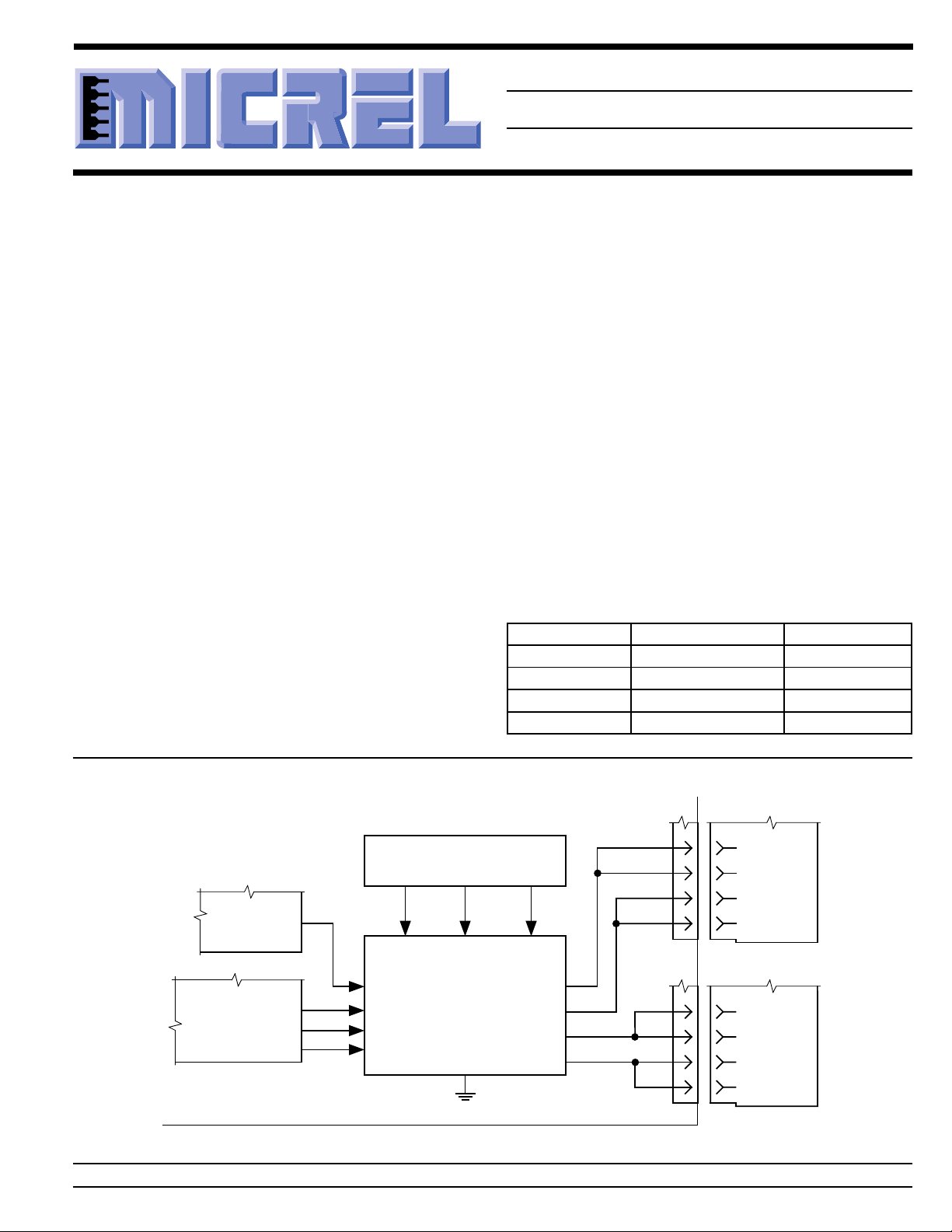
Typical Application
Slot A
Address and data lines
between logic controller and
PCMCIA cards not shown.
System Reset
Dual-Slot
Logic Controller
PCMCIA,
CardBus,
or Zoom Video
System Power Supply
(
OPTIONAL
)
12V
VPP IN
OPTIONAL
(
RST#
Serial
Control
Bus
V
)
MIC2564A
Power
Controller
3.3V
IN V
CC3
GND
OPTIONAL
(
5V
IN
CC5
OPTIONAL
(
A VPP OUT
A V
OUT
CC
B V
OUT
PP
B V
OUT
CC
)
)
Motherboard
PCMCIA Card Power Management Application
Micrel, Inc. • 1849 Fortune Drive • San Jose, CA 95131 • USA • tel + 1 (408) 944-0800 • fax + 1 (408) 944-0970 • http://www.micrel.com
September 1999 1 MIC2564A
V
1
PP
V
2
PP
V
CC
Slot B
1
V
PP
V
2
PP
V
CC
PCMCIA
Card
A
PCMCIA
Card
B
Page 2
MIC2564A Micrel
Pin Configuration
1V
CC5
CC5
IN
IN
2A VCC OUT
3V
4A FLAG
A V
V
CC3
A V
GND21
CC
CC
OUT24
IN23
OUT22
5SDA
6SCL
7RST#
8SLA
9B FLAG
10V
IN
CC5
B VCC OUT
V
CC5
11 14
12 13
IN
Pin Description
Pin Number Pin Name Pin Function
1,3,10,12 V
2,22,24 A V
4 A FLAG Channel A VCC and VPP Output Monitor (Output): Low on error condition.
5 SDA Serial Data (Input)
6 SCL Serial Clock (Input)
7 RST# System Reset (Input): Active low signal deactivates the MIC2564A, clearing
8 SLA Serial Data Latch (Input)
9 B FLAG Channel B VCC and VPP Output Monitor (Output): Low on error condition.
11,13,15 B V
14,23 V
16,21 GND Ground
17 B VPP OUT Slot B VPP Output
18,19 V
20 A VPP OUT Slot A VPP Output
IN 5V Supply Input: Optional system power supply connection. Required only
CC5
OUT Slot A VCC Output: Pins 2, 22, and 24 must be externally connected
CC
OUT Slot B VCC Output: Pins 11, 13, and 15 must be externally connected
CC
IN 3.3V Supply Input: Required system power supply connection. Powers 3.3V
CC3
IN 12V Supply Input: Optional system power supply connection. Required only
PP
A V
OUT20
PP
V
IN19
PP
18
17
16
15 B V
V
PP
B V
GND
V
CC3
B V
IN
PP
CC
IN
CC
OUT
OUT
OUT
24-lead SSOP (SM)
24-lead TSSOP (TS)
for 5V VCC and VPP output voltage.
together.
the serial registers and forcing the four power outputs to 0V (GND).
together.
VCC and VPP outputs and all internal circuitry.
for 12V VPP output voltage.
MIC2564A 2 September 1999
Page 3
MIC2564A Micrel
Absolute Maximum Ratings (Note 1)
VPP IN ......................................................................+13.6V
V
IN.......................................................................+6.0V
CC3
V
IN.......................................................................+6.0V
CC5
V
, V
, V
SCL
VA
FLAG
A or B V
A or B V
SDA
, VB
PP
CC
, V
SLA
.......................................................+6.0V
FLAG
OUT ....................... >120mA, Internally Limited
OUT .............................. >1A, Internally Limited
Power Dissipation at TA ≤ 25°C (PD) .......Internally Limited
Storage Temperature ............................... –65°C to +150°C
Lead Temperature (5 sec.)...................................... +260°C
ESD Rating, Note 3
....................................–0.3V to +6.0V
RST#
Operating Ratings (Note 2)
VPP IN ............................................................ 0V to +13.2V
V
IN........................................................ +3.0V to +5.5V
CC3
V
IN............................................................. 0V to +5.5V
CC5
V
, V
, V
SCL
A or B V
A or B V
SDA
PP
CC
, V
SLA
OUT ................................................0 to 120mA
OUT .......................................................0 to 1A
Clock Frequency .................................................0 to 2MHz
Ambient Temperature (TA).........................–40°C to +85°C
Junction Temperature (TJ) ...................................... +125°C
Package Thermal Resistance (θJA)
SSOP ..............................................................90˚C/W
................................. 0V to +5.5V
RST#
TSSOP ............................................................83˚C/W
Electrical Characteristics
V
Symbol Parameter Conditions Min Typ Max Units
VPP Output
I
PP
Hi-Z Leakage Current V
I
PPSC
R
VPP Switching Time (See Figure 2)
t
1
t
2
t
3
t
4
t
5
t
6
t
7
t
8
t
9
t
10
t
11
t
12
t
13
CC3 IN
= 3.3V, V
IN = 5.0V, VPP IN = 12V; TA = 25°C, bold indicates –40°C ≤ TA ≤ +85°C; unless noted.
CC5
OUT High Impedance Output shutdown mode 1 10 µA
OUT = 0V
PP
Short Circuit Current Limit V
O
Switch Resistance V
Output Turn-On Delay, Note 5 V
Output Rise Time V
Output Transition Time, Note 5 V
Output Turnoff Fall Time V
OUT = 0V, normal mode, Note 4 120 260 400 mA
PP
OUT = 5V selected, 1.6 5 Ω
PP
I
OUT = –100mA (sourcing)
PP
V
OUT = 3.3V selected, 1.3 5 Ω
PP
I
OUT = –100mA (sourcing)
PP
V
OUT = 12V selected, V
PP
I
OUT = –100 mA (sourcing)
PP
V
OUT = 0V [ground] selected, 2000 5000 Ω
PP
I
OUT = 50µA (sinking)
PP
OUT = Hi-Z to 10% of 3.3V, RL = 100Ω 1 100 µs
PP
V
OUT = Hi-Z to 10% of 5V, RL = 100Ω 1 100 µs
PP
V
OUT = Hi-Z to 10% of 12, RL = 100Ω 50 250 µs
PP
OUT = 10% to 90% of 3.3, RL = 100Ω 10 100 500 µs
PP
V
OUT = 10% to 90% of 5, RL = 100Ω 10 250 1000 µs
PP
V
OUT = 10% to 90% of 12, RL = 100Ω 10 100 500 µs
PP
OUT = 3.3V to 90% of 12V, RL = 100Ω 10 100 500 µs
PP
V
OUT = 5V to 90% of 12, RL = 100Ω 10 100 500 µs
PP
V
OUT = 12V to 90% of 3.3, RL = 100Ω 10 100 500 µs
PP
V
OUT = 12V to 90% of 5, RL = 100Ω 10 250 1000 µs
PP
OUT = 90% to 10% of 3.3, RL = 100Ω 1 500 µs
PP
V
OUT = 90% to 10% of 5, RL = 100Ω 1 500 µs
PP
V
OUT = 90% to 10% of 12, RL = 100Ω 1 500 µs
PP
IN = 12V, 1.3 2.3 Ω
PP
September 1999 3 MIC2564A
Page 4
MIC2564A Micrel
Symbol Parameter Conditions Min Typ Max Units
t
14
t
15
t
16
VCC Output
I
I
R
Hi-Z High Impedance Output shutdown mode, V
CC OUT
CCSC
O
VCC Switching Time (See Figure 3)
t
17
t
18
t
19
t
20
t
21
t
22
t
23
t
24
Power Supply
I
CC3
I
CC5
I
IN V
PP
V
CC3
V
CC5
V
PP
Thermal Shutdown
T
SD
Serial Interface DC Specifications
V
IH
V
IL
I
IN
Flag
I
FLG
Output Turnoff Delay Time, V
Notes 5, 7
OUT = 3.3V to Hi-Z, RL = 100Ω 150µs
PP
V
OUT = 5V to Hi-Z, RL = 100Ω 150µs
PP
V
OUT = 12V to Hi-Z, RL = 100Ω 150µs
PP
OUT = 0V 1 20 µA
CC
Leakage Current
Short Circuit Current Limit VCC OUT = 0, normal mode, 1.0 2.0 3.0 A
V
Switch Resistance V
Output Turn-On Delay Time, V
Note 5
Output Rise Time V
Output Fall Time V
Output Turnoff Delay, Notes 5, 6 V
V
IN Supply Current (3.3V) V
CC3
Note 7
V
IN Supply Current (5V) V
CC5
Note 8
IN Supply Current (12V) V
PP
Note 8
or V
CC3
OUT = 3.3V selected, 120 150 mΩ
CC
I
OUT = –1A (sourcing)
CC
OUT = 5V selected, 85 120 mΩ
V
CC
I
OUT = –1A (sourcing)
CC
OUT = 0V [ground] selected, 2000 3900 Ω
V
CC
I
OUT = 0.1mA (sinking)
CC
OUT = 0V to 10% of 3.3, RL = 10Ω 250 500 µs
CC
V
OUT = 0V to 10% of 5.0, RL = 10Ω 500 1000 µs
CC
OUT = 10% to 90% of 3.3V, RL = 10Ω 750 1200 5000 µs
CC
V
OUT = 10% to 90% of 5, RL = 10Ω 1000 2200 5000 µs
CC
OUT = 90% to 10% of 3.3, RL = 10Ω 100 550 1000 µs
CC
V
OUT = 90% to 10% of 5.0, RL = 10Ω 100 400 2000 µs
CC
OUT = 3.3V to 90% of 3.3V , RL = 10Ω 400 2000 µs
CC
V
OUT = 5V to 90% of 5V, RL = 10Ω 400 2000 µs
CC
OUT = 5V or 3.3V, I
CC
V
OUT = Hi-Z (sleep mode) 5 10 µA
CC
OUT = 5V or 3.3V, I
CC
V
OUT = Hi-Z (sleep mode) 0.2 10 µA
CC
OUT = 0V, 3.3V, 5V, or Hi-Z; I
PP
V
OUT = V
PP
switches, Note 4
CC5
OUT = 0 120 200 µA
CC
OUT = 0 25 50 µA
CC
OUT = 0 1 10 µA
PP
IN 4 50 µA
PP
Operating Input Voltage (3.3V) Note 7 3.0 3.3 5.5 V
Operating Input Voltage (5V) Note 8 — 5.0 5.5 V
Operating Input Voltage (12V) Note 8, 9 — 12 13.2 V
Thermal Shutdown Temperature 145 °C
Input Voltage: SDA, SCL, SLA pins
Input Voltage: SDA, SCL, SLA pins –0.3
0.7V
CC3
IN
5.5 V
0.3V
IN
CC3
V
Input Current 0V < VIN < 5.5V –1 0.2 1 µA
Flag Leakage Current V
= 5V 1 µA
FLG
MIC2564A 4 September 1999
Page 5

MIC2564A Micrel
Symbol Parameter Conditions Min Typ Max Units
Serial Interface Timing Requirements (See Figure 1), Note 10
t
HD:DAT
t
SU:DAT
t
SU:SLA
t
SU:RST#
t
W
Note 1. Exceeding the absolute maximum rating may damage the device.
Note 2. The device is not guaranteed to function outside its operating rating.
Note 3. Devices are ESD sensitive. Handling precautions recommended.
Note 4. Output enabled into short circuit.
Note 5. Measurement is from the 50% point of the SLA rising edge.
Note 6. Measurement is from the Hi-Z- or 0V-state command to the beginning of the slope. Measurement does not apply when device is in current
Note 7. V
Note 8. V
Note 9. V
Note 10. Guaranteed by design not production tested.
SDA Hold Time 75 ns
SDA Setup Time data before clock 75 ns
Latch Setup Time 50 ns
Reset to Data Setup Time RST# before data 50 ns
Minimum Pulse Width clock (t
latch (t
reset (t
data (t
limit or thermal shutdown.
IN powers all internal logic, bias, and drive circuitry, and is required for operation.
CC3
and V
PP
IN must be either high impedance or greater than or approximately equal to the highest voltage V
PP
3.3V and 5V are connected to the MIC2564A, V
IN are not required for operation.
CC5
IN must be either 5V, 12V, or high impedance.
PP
)50ns
W:CLK
) 100 ns
W:SLA
)50ns
W:RST
)50ns
W:DA
in the system. For example, if both
CC
Serial Control Timing Diagram
t
W:DAT
RST#
t
SU:RST#
SDA
SLA
SCL
The MIC2564A uses a three-wire serial interface to control VCC and VPP outputs for both sections A and B. The three control
lines have thresholds compatible with both 3.3V and 5V logic families. Data (SDA) is clocked in on the rising clock edge. The
clock signal may be continuous or it may halt after all data is clocked in.
D8 D7 D6 D5 D4 D3 D2 D1 D0
t
SU:DAT
t
HD:DAT
t
W:CLK
t
Figure 1. Serial Control Timing Diagram
SU:SLA
t
W:SLA
September 1999 5 MIC2564A
Page 6

MIC2564A Micrel
Output Timing Diagrams
V
PP
Enable
12V
V
PP
OUT
5V
3.3V
AB CD
0
VPP to 3.3V VPP to 12V
t
7
t
t
4
1
t
9
t
EF G JH
VPP to 5VVPP to 3.3VVPP to 12V
PP
OFF
t
2
t
t
11
5
14
0
K
V
t
12
to 12V VPP OFF
PP
t
6
t
3
t
13
t
16
V
to 5VV
PP
t
8
t
10
V
PP
OFF
t
15
FLAG
Figure 2. VPP Timing Diagram
VPP Enable is shown generically. RL = 100Ω. CL = negligible. Refer to the serial control timing diagrams for details.
At time A)VPP = 3.3V is selected, B)VPP is set to 12V, C)VPP = 3.3V (from 12V), D)VPP is disabled, E)VPP is programmed
to 5V, F)VPP is set to 12V, G)VPP is programmed to 5V, H)VPP is disabled, J)VPP is set to 12V, K)VPP is again disabled.
ABC D
V
CC
Enable
0
VCC to 3.3V VCC to 5VVCC OFF VCC OFF
V
CC
OUT
FLAG
5V
3.3V
0
0
t
17t19
t23t
21
t
t
18
20
t24t
22
Figure 3. VCC Timing Diagram
VCC Enable is shown generically. RL = 10Ω. Refer to the serial control timing diagrams for specific control logic input.
At time A)VCC is programmed to 3.3V, B)VCC is disabled, C)VCC is programmed to 5V, D)VCC is disabled.
MIC2564A 6 September 1999
Page 7

MIC2564A Micrel
OUT
CC
OUT A V
PP
OUT A V
CC
OUT B V
PP
B V
PP_PGM
A V
†
0V*
†
†
†
0V
†
0V*
†
†
0V*
†
PP_VCC
3A V
CC
5A V
CC
A V
PP_PGM
B V
PP_VCC
3B V
CC
.
The PC Card Specification
illegal state per
†
5B V
CC
0XXXXXXXX Hi-Z Hi-Z Hi-Z Hi-Z
1 0000 0V*0V*
1 0001 12V
1 0010 0V*0V*
1 0011 Hi-Z 0V*
1 0100 0V*3.3V
1 0101 12V3.3V
1 0110 3.3V3.3V
1 0111 Hi-Z 3.3V
1 1000 0V*5V
1 1001 12V5V
1 1010 5V5V
1 1011 Hi-Z 5V
1 1100 0V*0V*
1 1101 12V
1 1110 0V*0V*
1 1111 Hi-Z 0V*
10000 0V*0V*
10001 12V
10010 0V*0V*
10011 Hi-Z 0V*
10100 0V*5V
10101 12V5V
10110 5V5V
10111 Hi-Z 5V
11000 0V*3.3V
11001 12V3.3V
11010 3.3V 3.3V
11011 Hi-Z 3.3V
11100 0V*0V*
11101 12V
11110 0V*0V*
D8 D7 D6 D5 D4 D3 D2 D1 D0
MIC2564A-0 Logic T able
SHDN B V
11111 Hi-Z 0V*
X = don’t care, * clamped to ground,
September 1999 7 MIC2564A
Page 8

MIC2564A Micrel
OUT
CC
OUT A V
PP
OUT A V
CC
OUT B V
PP
B V
PP_PGM
A V
†
†
0V*
†
†
0V
†
0V*
†
†
0V*
†
PP_VCC
3A V
CC
5A V
CC
A V
PP_PGM
B V
PP_VCC
3B V
CC
.
The PC Card Specification
illegal state per
†
5B V
CC
0XXXXXXXX Hi-Z Hi-Z Hi-Z Hi-Z
1 0000 0V*0V*
1 0001 12V
1 0010 0V*0V*
1 0011 Hi-Z 0V*
1 0100 0V*3.3V
1 0101 12V3.3V
1 0110 3.3V 3.3V
1 0111 5V3.3V
1 1000 0V*5V
1 1001 12V5V
1 1010 5V5V
1 1011 3.3V 5V
1 1100 0V*0V*
1 1101 12V
1 1110 0V*0V*
1 1111 Hi-Z 0V*
10000 0V*0V*
10001 12V
10010 0V*0V*
10011 Hi-Z 0V*
10100 0V*5V
10101 12V5V
10110 5V5V
10111 3.3V5V
11000 0V*3.3V
11001 12V3.3V
11010 3.3V 3.3V
11011 5V3.3V
11100 0V*0V*
11101 12V
11110 0V*0V*
D8 D7 D6 D5 D4 D3 D2 D1 D0
MIC2564A-1 Logic T able
SHDN B V
11111 Hi-Z 0V*
X = don’t care, * clamped to ground,
MIC2564A 8 September 1999
Page 9

MIC2564A Micrel
Functional Diagram
V
SDA
SCL
RST#
SLA
Gate-Drive
Charge Pump
CC3
3.3V
IN
IN
V
CC5
5V
(optional)
VPP IN
12V
(optional)
A V
B V
PP
PP
OUT
OUT
A FLAG
B FLAG
Control
Logic
Current
Limit
Thermal
Shutdown
GND
MIC2564
A V
B V
CC
CC
OUT
OUT
September 1999 9 MIC2564A
Page 10

MIC2564A Micrel
Applications Information
PC Card power control for two sockets is easily accomplished
using the MIC2564A PC Card/CardBus power controller.
Control commands from a three-wire (plus Reset) serial bus
determine VCC and VPP output voltages and select standby
or operate mode.
VCC outputs of 3.3V and 5V at the maximum allowable PC
Card current are supported. The VCC outputs also support
GND (0V) and high-impedance states. The VPP outputs
support VPP (12V), VCC voltages (3.3V or 5V), GND (0V), or
high impedance. When the VCC = Hi-Z (high impedance)
condition is selected, the device switches into sleep mode
and draws only leakage current.
Full protection during hot switching is provided which prevents feedback from the V
supply into the 3.3V supply) by locking out the low voltage
switch until the initial switch’s gate voltage drops below 0.7V.
MIC2564A internal logic and MOSFET drive circuitry is
powered from the V
voltage multipliers. Switching speeds are carefully controlled
to prevent damage to sensitive loads and meet all PC Card
Specification timing requirements, including those for the
CardBus option.
Supply Bypassing
The MIC2564A is a switch and has no stability problems;
however, supply bypass capacitors are recommended to
reduce inductive transients and improve output ripple. As all
internal device logic and comparison functions are powered
from the V
input, the power supply quality on this line is the
CC3
most important. Micrel recommends placing 1µF surfacemount ceramic (low ESR) capacitors from V
V
IN pins to ground and two 0.1µF surface-mount ceramic
CC5
capacitors, one from each VPPIN pin, to ground. Also, the
VCCOUT and VPPOUT pins may use 0.01µF to 0.1µF
capacitors for noise reduction and to reduce the chance of
ESD (electrostatic discharge) damage.
Power Status Feedback (Flags)
Two flag outputs monitor the VCC and VPP output voltages on
both slot A and B, falling low when the voltage is not proper.
Use of these open-drain flag outputs is optional; if they are
used, a pull-up resistor to either the 3.3V or 5V supply is
required. Unused flag outputs may be left open.
PC Card Slot Implementation
The MIC2564A is designed for full compatibility with the
Personal Computer Memory Card International Association
(PCMCIA) PC Card Specification including the CardBus and
Zoom Video (ZV) options.
When a PC card is initially inserted, it should receive V
(3.3V ± 0.3V or 5.0V ±5%). The initial voltage is determined
by a combination of mechanical socket keys and voltage
sense pins. The card sends a handshaking data stream to the
logic controller, which then determines if this card requires
VPP and if the card is designed for dual VCC. If the card is
compatible with, and requires, a different V
controller commands the power controller to make this change
by disabling VCC, waiting at least 100ms, and then reenabling the other VCC voltage.
output (for example, from the 5V
CC
input and internal charge-pump
CC3
CC3
level, the logic
CC
IN and
CC
If no card is inserted, or the system is in sleep mode, the logic
controller commands the MIC2564A to shut down VCC. This
also places the switch into a shutdown (sleep) mode, where
current consumption drops to nearly zero, with only tiny
CMOS leakage currents flowing.
Internal device control logic, MOSFET drive and bias voltage
is powered from V
IN. The high voltage bias is generated
CC3
by an internal charge pump multiplier. Input logic threshold
voltages are compatible with common PC Card logic controllers using either 3.3V or 5V supplies.
PC Card Voltage Regulation
The MIC2564A has been designed to meet or exceed PC
Card voltage regulation specifications. The on-resistance of
the FET switches will meet regulation requirements at 600mA
and 1A respectively for VCC = 5V ±3% and 3.3V ±3%.
Flash Memory Implementation
When programming flash memory (standard +12V flash
memories), the PC Card slot logic controller enables VPP on
the MIC2564A, which connects VPPIN (nominally +12V) to
VPPOUT. The low on-resistance of the MIC2564A switch
allows using a small bypass capacitor on the VPPOUT pins,
with the main filtering performed by a large filter capacitor on
VPPIN. (Usually the main power supply filter capacitor is
sufficient.) Using a small-value capacitor such as 0.1µF on
the output causes little or no timing delays.
The VPPOUT transition from VCC to 12.0V typically takes
200µs. After programming is completed, the logic controller
signals to the MIC2564A, which then reduces VPPOUT to the
VCC level. Break-before-make switching action and controlled rise times reduce switching transients and lower
current spikes through the switch.
Output Current and Protection
The MIC2564A meets or exceeds all PCMCIA specifications.
MIC2564A output switches are capable of passing the maximum current needed by any PC Card. For system and card
protection, output currents are internally limited. For full
system protection, long term (longer than a few milliseconds)
output short circuits invoke overtemperature shutdown, protecting the MIC2564A, the system power supplies, the card
socket pins, board traces, and the PC Card. Individual
internal status registers for each slot indicate when power
problems exist.
Control Bus Interface Overview
The MIC2564A power controller communicates with a logic
controller (host adapter) via a 3-wire serial interface. A fourth
control line attaches to the system reset line (RST#) and
places all MIC2564A switches in the high impedance (off)
state. The reset function is active low.
MIC2564A 10 September 1999
Page 11

MIC2564A Micrel
Slot A
Controller
(3.3V or 5V)
Generic
PCMCIA/CardBus
Host Adapter
VCC
A PGOOD
B PGOOD
SDATA
SCLK
SLATCH
RST#
Power
2
330k
System Reset
1.0µF 1.0µF
V
CC3
4
A FLG
9
B FLG
5
SDA
6
SCL
8
SLA
7
RST#
IN V
MIC2564A
Power
Controller
16, 21
ceramicceramic ceramic
IN VPP IN
CC5
GND
+12V+5V+3.3V
0.1µF
18, 191, 3, 1014, 23
A VPP OUT
OUT
A V
CC
OUT
B V
PP
B V
OUT
CC
0.1µF
20
2, 22, 24
17
11, 13, 15
0.01µF
0.01µF
0.01µF
0.01µF
VPP1
2
V
PP
V
CC
Slot B
VPP1
2
V
PP
V
CC
Cirrus Logic
CL-PD6832/33
SDATA
SCLK
SLATCH
RST#
Figure 4. Generic “3-Wire” Serial Control Interface
+12V+5V+3.3V
0.1µF
ceramicceramic ceramic
18, 191, 3, 1014, 23
OUT
OUT
OUT
20
2, 22, 24
17
11, 13, 15
A VPP OUT
A V
CC
B V
PP
B V
CC
0.01µF
0.01µF
131
132
130
207
1.0µF 1.0µF 0.1µF
V
5
6
8
7
SDA
SCL
SLA
RST#
IN V
CC3
MIC2564A
Controller
CC5
Power
GND
16, 21
IN VPP IN
System
Reset
Figure 5. Cirrus Logic CL-PD6832 and CL-PD6833 Interface
0.01µF
0.01µF
Slot A
VPP1
2
V
PP
V
CC
Slot B
VPP1
2
V
PP
V
CC
September 1999 11 MIC2564A
Page 12

MIC2564A Micrel
Slot A
+12V+5V+3.3V
1.0µF 1.0µF 0.1µF
0.1µF
ceramicceramic ceramic
VPP1
V
PP
2
O2 Micro
OZ6833
OZ6933
CPWRDATA
CPWRCLK
CPWRLATC
RST#
O2 Micro
OZ6860
SDATA
SCLK
SLATCH
RST#
131
132
130
207
System
Reset
116
118
115
250
System
Reset
18, 191, 3, 1014, 23
V
5
6
8
7
SDA
SCL
SLA
RST#
IN V
CC3
MIC2564A
Controller
CC5
Power
GND
16, 21
IN VPP IN
A VPP OUT
A V
CC
B V
PP
B V
CC
OUT
OUT
OUT
20
2, 22, 24
17
11, 13, 15
Figure 6. O2 Micro OZ6833 and OZ6933
+12V+5V+3.3V
1.0µF 1.0µF 0.1µF
V
5
6
8
7
SDA
SCL
SLA
RST#
IN V
CC3
MIC2564A
Controller
CC5
Power
GND
16, 21
IN VPP IN
0.1µF
ceramicceramic ceramic
18, 191, 3, 1014, 23
OUT
OUT
OUT
20
2, 22, 24
17
11, 13, 15
A VPP OUT
A V
CC
B V
PP
B V
CC
0.01µF
0.01µF
0.01µF
0.01µF
0.01µF
0.01µF
0.01µF
0.01µF
V
CC
Slot B
VPP1
2
V
PP
V
CC
Slot A
VPP1
2
V
PP
V
CC
Slot B
VPP1
2
V
PP
V
CC
Figure 7. O2 Micro OZ6860
MIC2564A 12 September 1999
Page 13

MIC2564A Micrel
(
Package Dimensions
0.875 (0.034) REF
8.33 (0.328)
8.07 (0.318)
0.38 (0.015)
0.25 (0.010)
0.65 (0.0260) BSC
5.40 (0.213)
5.20 (0.205)
7.90 (0.311)
7.65 (0.301)
2.00 (0.079)
1.73 (0.068)
0.21 (0.008)
0.05 (0.002)
COPLANARITY:
0.004) MAX
0.10
24-pin SSOP (SM)
0°
–8°
10°
4°
DIMENSIONS:
MM (INCH)
0.22 (0.009)
0.13 (0.005)
1.25 (0.049) REF
0.95 (0.037)
0.55 (0.022)
0.30 (0.012)
0.19 (0.007)
7.90 (0.311)
7.70 (0.303)
0.65 BSC
(0.026)
4.50 (0.177)
4.30 (0.169)
0.15 (0.006)
0.05 (0.002)
6.4 BSC (0.252)
1.10 MAX (0.043)
8°
0°
24-pin TSSOP (TM)
DIMENSIONS:
MM (INCH)
0.20 (0.008)
0.09 (0.003)
1.00 (0.039) REF
0.70 (0.028)
0.50 (0.020)
September 1999 13 MIC2564A
Page 14

MIC2564A Micrel
MIC2564A 14 September 1999
Page 15

MIC2564A Micrel
September 1999 15 MIC2564A
Page 16

MIC2564A Micrel
MICREL INC. 1849 FORTUNE DRIVE SAN JOSE, CA 95131 USA
TEL + 1 (408) 944-0800 FAX + 1 (408) 944-0970 WEB http://www.micrel.com
This information is believed to be accurate and reliable, however no responsibility is assumed by Micrel for its use nor for any infringement of patents or
other rights of third parties resulting from its use. No license is granted by implication or otherwise under any patent or patent right of Micrel Inc.
© 1999 Micrel Incorporated
MIC2564A 16 September 1999
 Loading...