

Page 1
1
The MIC1832 is a multifunction circuit which monitors
microprocessor activity, external reset and power
supplies in microprocessor based systems. The circuit
functions include a watchdog timer, power supply
monitor, microprocessor reset, and manual pushbutton
reset input.
The power supply line is monitored with a comparator
and an internal voltage reference. RST is forced low
when an out-of-tolerance condition exists and remains
asserted for at least 250ms after V
CC
rises above the
threshold voltage (2.55V or 2.88V). The RST pin will
remain logic low with V
CC
as low as 1.4V.
The Watchdog input (ST) monitors µP activity and will
assert RST if no µP activity has occurred within the
watchdog timeout period. The watchdog timeout period
is selectable with a nominal periods of 150, 600, or
1200 milliseconds.
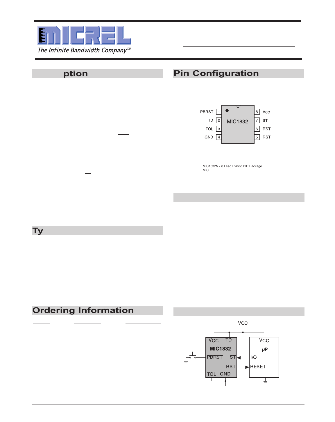
MIC1832N - 8 Lead Plastic DIP Package
MIC1832M - 8 Lead Plastic SOIC Package
Part Package Temp. Range
MIC1832N 8-Lead PDIP -40°C to +85°C
MIC1832M 8-Lead SOIC -40°C to +85°C
·
Automotive Systems
·
Intelligent Instruments
·
Critical Microprocessor Power Monitoring
·
Battery Powered Computers
·
Controllers
·
Power OK/Reset Time Delay, 250ms min.
·
Watchdog Timer, 150ms, 600ms, or
1.2s typical
·
Precision Supply Voltage Monitor, Select
Between 5% or 10% of Supply Voltage
·
Available in 8-pin Surface Mount (SO)
·
Debounced External Reset Input
·
Low Supply Current,
< 18µA Typ.
Typical Operating Circuit
Features
Description
Pin Configuration
Ordering Information
Typical Applications
Top View
MIC1832 µP Supervisory Circuit
MIC1832
µP Supervisory Circuit
PBRST
1
TD
2
MIC1832
TOL
3
GND
4
8
V
CC
7
ST
RST
6
RST
5
V
CC
TD
V
CC
MIC1832
PBRST
GND
TOL
ST
RST
V
I/O
RESET
CC
µP
Page 2
MIC1832 µP Supervisory Circuit
2
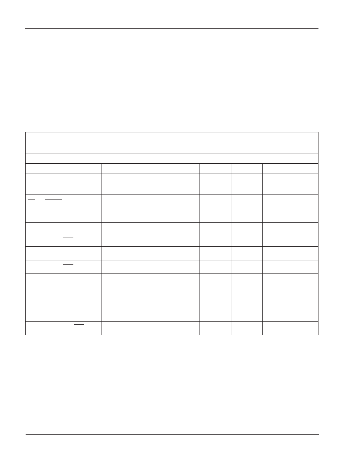
Electrical Characteristics
VCC= 3 to 5.5 V, TA= Operating Temperature Range, unless otherwise noted.
Parameter Conditions Min Typ Max Units
Supply Voltage Range V
CC
5.5 V
Supply Current I
CC
@ V
CC
= 5V (See Note 1) 18 30 µA
I
CC
@ V
CC
= 3.3V (See Note 1) 15 25 µA
ST and PBRST Input Levels V
IH
(See Note 2)
2.0
VCC+ 0.3 V
V
IH
(See Note 3)
VCC - 0.4
VCC+ 0.3 V
V
IL
-0.3 0.5
Input Leakage, ST (See Note 4) I
IL ±1
µA
Output Voltage, RST, RST I
SOURCE
= 350µA, V
CC
= 3.3V 2.4 V
Output Voltage, RST, RST I
SINK
= 10mA, VCC= 3.3V 0.4 V
Output Voltage, RST V
CC
= 1.4V, I
SINK
= 50µA 0.3 V
V
CC
5% Trip Point (Reset TOL = Gnd 2.80 2.88 2.97 V
Threshold Voltage)
V
CC
10% Trip Point (Reset TOL = V
CC
2.47 2.55 2.64 V
Threshold Voltage)
Input Capacitance, ST, TOL C
IN
(See Note 5) 5 pF
Output Capacitance, RST, RST C
OUT
(See Note 5) 7 pF
Absolute Maximum Ratings
Terminal Voltage
VCC, . . . . . . . . . . . . . . . . . . . . . . . . . . . -0.3V to 7.0V
All Other Inputs . . . . . . . . . . . . -0.3V to (VCC+ 0.3V)
Input Current
VCC. . . . . . . . . . . . . . . . . . . . . . . . . . . . . . . . 250mA
Gnd, All Other Inputs . . . . . . . . . . . . . . . . . . . . 25mA
Operating Temperature Range
MIC1832_ . . . . . . . . . . . . . . . . . . . . . . . . . -40°C to 85°C
Storage Temperature Range . . . . . . . . . . . . .-65°C to 150°C
Lead Temperature (Soldering - 10 sec.) . . . . . . . . . . . 300°C
Power Dissipation . . . . . . . . . . . . . . . . . . . . . . . . . . 700mW
Stresses above those listed under ABSOLUTE MAXIMUM RATINGS may cause permanent device failure. Functionality at or above these limits is not implied. Exposure to absolute
maximum ratings for extended periods may affect device reliability. Operating ranges define those limits between which the functionality of the device is guaranteed.
Page 3
MIC1832 µP Supervisory Circuit
3
Note 1: ICCis measured with PBRST and all outputs open and inputs within 0.5V of supply rails.
Note 2: Measured with VCC ≥ 2.7V.
Note 3: Measured with VCC < 2.7V.
Note 4: PBRST has an internal pull-up resistor to V
CC
(typ. 40kΩ).
Note 5: Guaranteed by design at TA= 25
°C.
Note 6: PBRST must be held low for a minimum of 20ms to guarantee a reset.
Note 7: V
CC
falling at 8.5mv/µs.
A.C. Electrical Characteristics
VCC= 3 to 5.5 V, TA= Operating Temperature Range, unless otherwise noted.
Parameter Conditions Min Typ Max Units
PBRST Min. Pulse Width, t
PB
PBRST = VIL(see note 6) 20 ms
PBRST Delay, t
PBD
1 4 20 ms
Reset Active Time, t
RST
250 610 1000 ms
ST Pulse Width, t
ST
20 ns
ST Timeout Period, t
TD
TD = 0V 62.5 150 250 ms
TD = Open 250 600 1000
TD = V
CC
500 1200 2000
VCCFall Time, t
F
40
µs
VCCRise Time, t
R
0
ns
VCCDetect to RST Low V
CC
Falling (see note 7) 5 8 µs
and RST High, t
RPD
VCCDetect to RST High VCCRising 250 610 1000 ms
and RST Low, t
RPU
Page 4

4
Pin 1: PBRST - Pushbutton reset input. This input is debounced and can be driven with external logic signals or by
means of a mechanical pushbutton to actively force a reset. All pulses less than 1ms in duration on the
PBRST pin are ignored, whereas, any pulse with a duration of 20ms or greater is guaranteed to cause a
reset. PBRST has an internal pull-up resistor to V
CC
of 40kΩ typical.
Pin 2: TD - Time delay input. This input selects the timebase used by the watchdog timer. When TD = 0V, the
watchdog timeout period is set to a nominal value of 150ms and when TD = open, the watchdog timeout
period is set to a nominal value of 600ms and when TD = VCC, the watchdog timeout period is 1.2sec
nominally.
Pin 3: TOL - Tolerance select input. Selects whether 5% or 10% of VCCis used as the reset threshold voltage.
When TOL = 0V, the 5% tolerance level is selected and when TOL = VCC, a 10% tolerance level is selected.
Pin 4: GND - IC ground pin, 0V reference.
Pin 5: RST - RST is asserted high if either VCCgoes below the reset threshold, the watchdog times out or PBRST is
pulled low for a minimum of 20ms. RST remains asserted for one reset timeout period after VCCexceeds the
reset threshold or after the watchdog times out or after PBRST goes high.
Pin 6: RST - RST is asserted low if either VCCgoes below the reset threshold, the watchdog times out or PBRST is
pulled low for a minimum of 20ms. RST remains asserted for one reset timeout period after VCCexceeds the
reset threshold or after the watchdog times out or after PBRST goes high.
Pin 7: ST - Input to the watchdog timer. If ST does not see a transition from high to low within the watchdog timeout
period, RST and RST will be asserted.
Pin 8: VCC- Primary supply input.
Pin Functions
MIC1832 µP Supervisory Circuit
Page 5

5
+
-
REF
WATCHDOG
TIMER
VCC(8)
GND (4)
RST (5)
TD (2)
RST (6)
RESET
GENERATOR
ST (7)
TIMEOUT
SELECT
PBRST (1)
MANUAL RESET
DEBOUNCE
TRIP POINT
SELECT
TOL (3)
Block Diagram
Table 1. Watchdog Timeout Period
Circuit Description
t
TD
TD Pin Min. Typ. Max.
Gnd 62.5ms 150ms 250ms
Open 250ms 600ms 1000ms
V
CC
500ms 1200ms 2000ms
MIC1832 µP Supervisory Circuit
Page 6

6
Power Monitor
The RST and RST pins are asserted whenever V
CC
falls below the reset threshold voltage as determined by
the TOL pin. A 5% tolerance level (2.88V reset
threshold voltage) can be selected by connecting the
TOL pin to ground and a 10% tolerance (2.55V reset
threshold voltage) can be selected by connecting the
TOL pin to VCC. The reset pins will remain asserted for
a period of 250ms after VCChas risen above the reset
threshold voltage. The reset function ensures the
microprocessor is properly reset and powers up into a
known condition after a power failure. RST will remain
valid with VCCas low as 1.4V.
Watchdog Timer
The microprocessor can be monitored by connecting
the ST pin (watchdog input) to a bus line or I/O line. If a
high-to-low transition doesn’t occur on the ST pin within
the watchdog timeout period (determined by TD pin, see
Table 1), the RST and RST pins will be asserted
resulting in a microprocessor reset. RST and RST will
remain asserted for at least 250ms when this occurs. A
minimum pulse of 75ns or any transition high-to-low on
the ST pin will reset the watchdog timer. The watchdog
timer will be reset if ST sees a valid transition within the
watchdog timeout period.
Pushbutton Reset Input
The PBRST input can be driven with a manual
pushbutton switch or with external logic signals. The
input is internally debounced and requires an active low
signal to force the reset outputs into their active states.
The PBRST input will recognize any pulse that is 20ms
in duration or greater and will ignore all pulses that are
less than 1ms in duration.
Figure 1. Power-Up/Power-Down Sequence
Circuit Description
Figure 3. Pushbutton Reset
Figure 2. Watchdog Input
Note: The maximum time between high-to-low transitions (tTD) on the
watchdog input (ST) is determined by the voltage applied to the
TD pin. If the watchdog input sees a high-to-low transition prior to
the timeout period, the watchdog timer will be reset.
MIC1832 µP Supervisory Circuit
V
CC
RST
RST
V
CCTP
t
RPD
V
CCTP
t
RPU
t
ST
ST
t
TD
t
PB
t
PDLY
PBRST
t
RST
RST
RST
Page 7

7
Alternate Source Cross Reference Guide
MIC Direct
Industry P/N Replacement
DS1832 MIC1832NC
DS1832S MIC1832MC
MIC1832 µP Supervisory Circuit
Page 8

8
Packaging Information
M Package, 8-Pin Small Outline
N Package, 8-Pin Plastic Dual-In-Line
MIC1832 µP Supervisory Circuit
0.197
0.190
0.244
Pin 1 Identifier
0.155
0.150
0.228
0.012
0.009
0.019
0.013
0.060
0.040
0.011
0.004
0.069
0.053
0.400
0.370
0.260
0.240
0.035
0.015
0.150
0.125
0.023
0.015
0.110
0.090
0.150
0.120
0.050
0.016
0.310
0.290
0.370
0.300
0-8¼
 Loading...