

Datasheet MIC1555YD5, MIC1555YM5, MIC1555YMU, MIC1557YD5, MIC1557YM5 Datasheet (Micrel) [ru]
Page 1

IttyBitty is a registered trademark of Micrel, Inc.
August 12
General Description
The MIC1555 IttyBitty® CMOS RC timer/oscillator and
MIC1557 IttyBitty
provide rail-to-rail pulses for precise time delay or
frequency generation.
The devices are similar in func tion to the industr y standard
“555”, without a frequency control (FC) pin or an opencollector discharge (D) pin. The threshold pin (THR) has
precedence over the trigg er (TRG) input, ensuring that the
BiCMOS output is off when TRG is high.
The MIC1555 can be used as an astable (oscillator) or
monostable (one-shot) with separate thresho ld and trigger
inputs. In the one-shot mode, the output pulse width is
precisely controlled by an external resistor and a capacitor.
Time delays may be accurately controlled from microseconds to hours. In the oscillator mode, the output is
used to provi de precise feedback, with a m inimum of one
resistor and one capacitor producing a 50% duty cycle
square wave.
The MIC1557 is designe d for astable (osc illator) operatio n
only, with a chip select/r eset (CS) input for low po wer shutdown. One resistor and one capacitor provide a 50% duty
cycle square wave. Other duty-cycle ratios may be
produced using two diodes and two resistors.
The MIC1555/7 is powere d from a +2.7V to +18V supply
voltage and is rated for –40°C to +85°C ambient
temperature range. T he MIC 155 5/7 is available in SOT-235, and thin SOT23-5 5-pin packages. A low profil e, ultrathin, (UTDFN), version of the MIC1555 (with c hip selec t) is
also available.
Datasheets and support documentation are available on
Micrel’s website at: www.micrel.com
®
CMOS RC oscillator are designed to
.
MIC1555/1557
IttyBitty® RC Timer/Oscillator
Features
• +2.7V to +18V operation
• Low current
− <1µA typical shutdown mode (MIC1557)
− 200µA typical (TRG and THR low) at 3V supply
• Timing from microseconds to hours
• “Zero” leakage trigger and threshold inputs
• 50% square wave with one resistor, one capacitor
• Threshold input precedence over trigger input
• <15Ω output on resistance
• No output cross-conduction current spikes
• <0.005%/°C temperature stability
• <0.055%/V supply stability
• 10-pin ultra-thin DFN package (2mm × 2mm × 0.4mm)
• Small SOT-23-5 surface mount package
Applications
• Precision timer
• Pulse generation
• Sequential timing
• Time-delay generation
• Missing pulse detector
• Micropower oscillator to 5MHz
• Charge-pump driver
• LED blinker
• Voltage converter
• Linear sweep generator
• Variable frequency and duty cycle oscillator
Micrel Inc. • 2180 Fortune Drive • San Jose, CA 95131 • USA • tel +1 (408) 944-0800 • fax + 1 (408) 474-1000 • http://www.micrel.com
, 2015
Revision 6.1
Page 2
Micrel, Inc.
MIC1555/1557
August 12
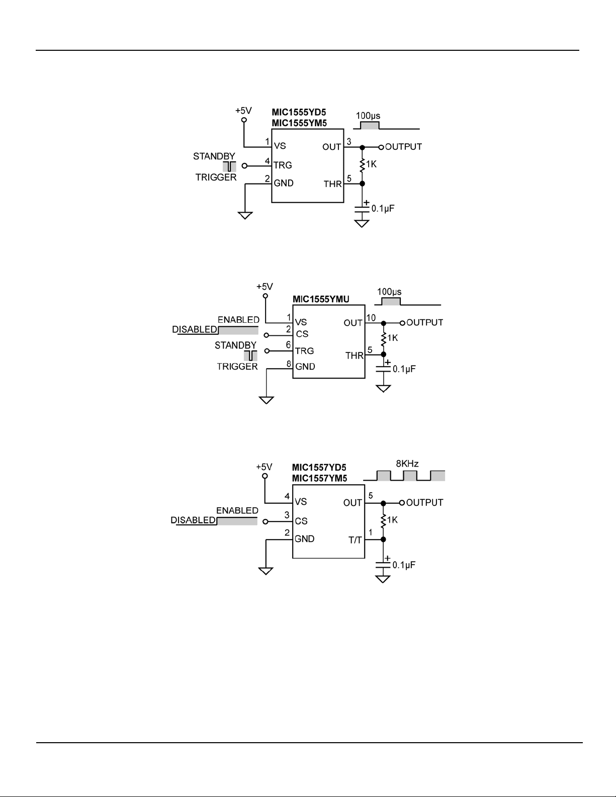
Typical Applications
Monostable (One-Shot)
Monostable (with Enable)
Astable (Oscillator)
, 2015 2
Revision 6.1
Page 3
Micrel, Inc.
MIC1555/1557
August 12
(1, 2)
(Top View)
(Top View)
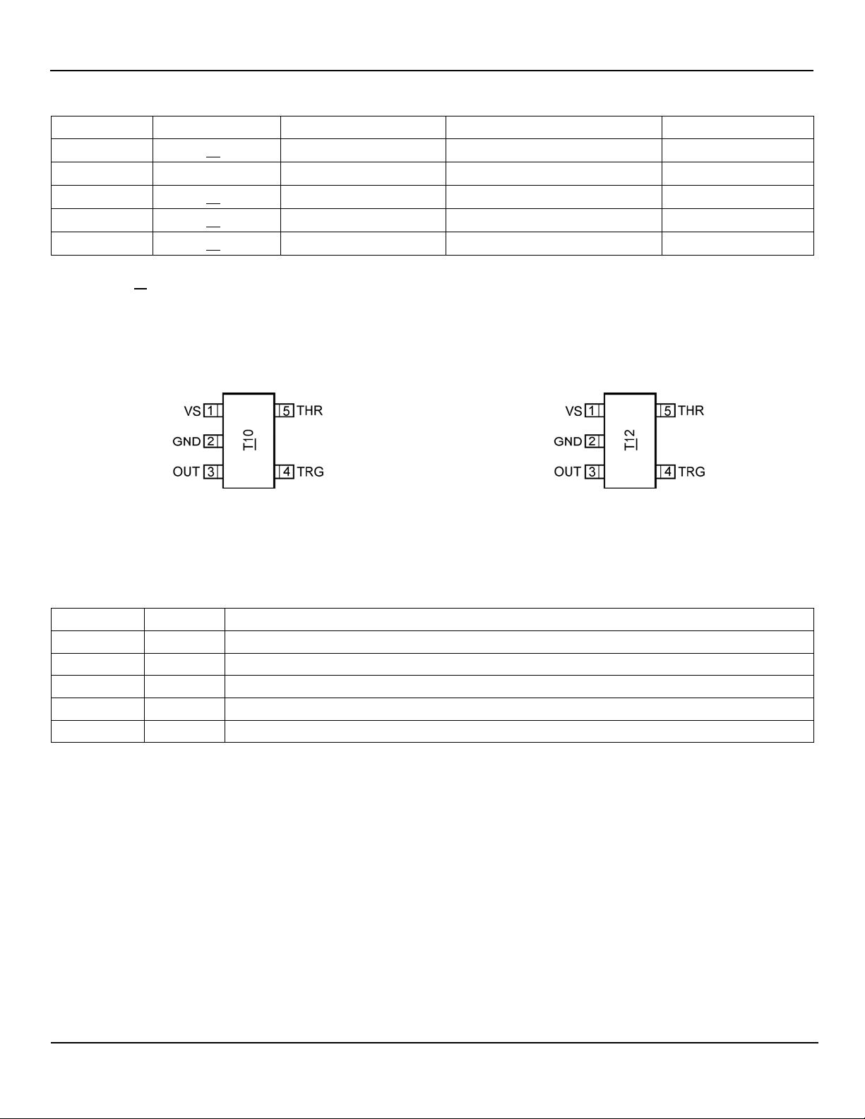
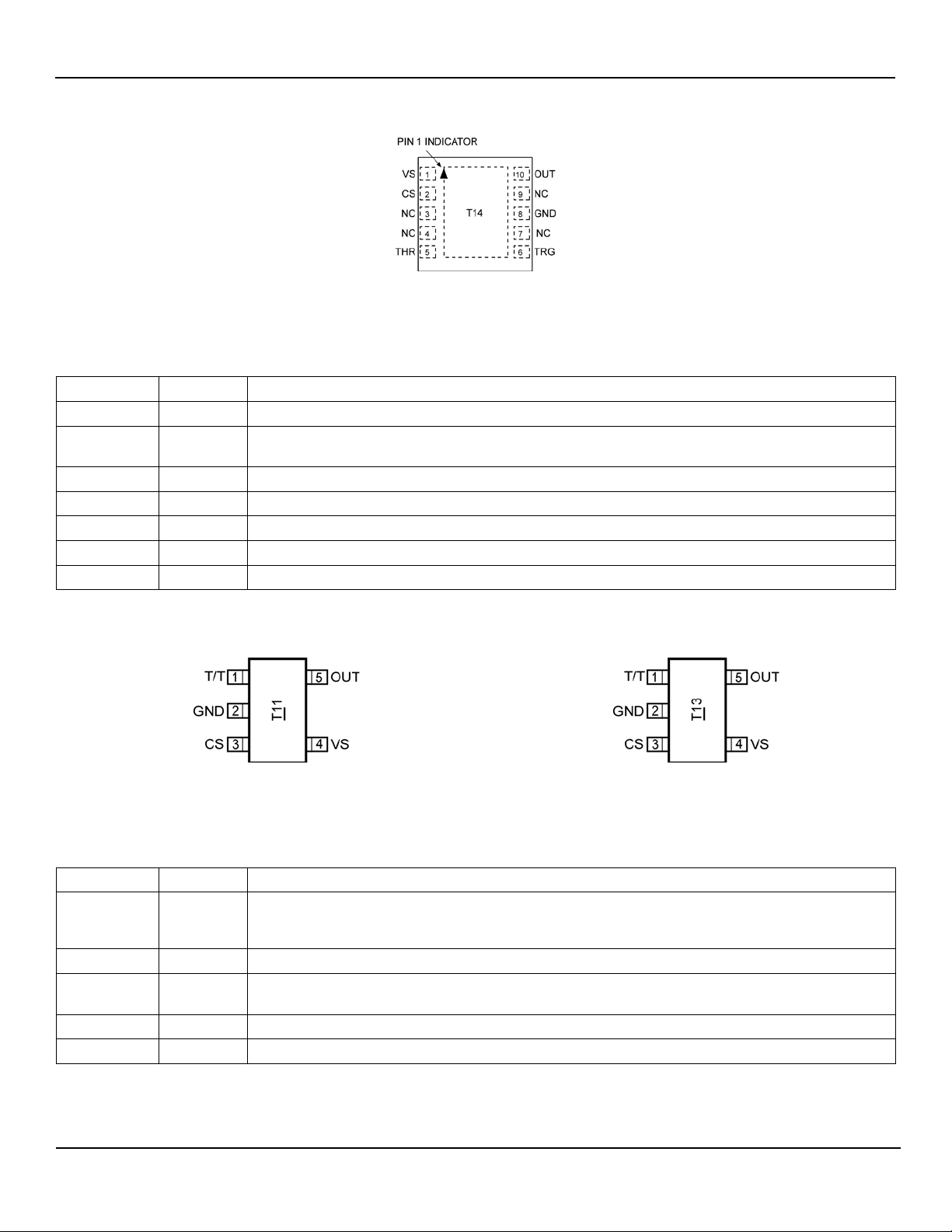
Ordering Information
Part Number Top Marking
MIC1555YD5 T12
MIC1555YMU T14
MIC1555YM5 T10
MIC1557YD5 T13
MIC1557YM5 T11
Note:
1. Underbars ( ) shown for the top marking may not be to scale.
2. The top marking in the YMU package does not have an underbar.
Temperature Range Package Package Height (mm)
–40°C to +85°C
–40°C to +85°C
–40°C to +85°C
–40°C to +85°C
–40°C to +85°C
10-Pin 2mm × 2mm UTDFN 0.4 (maximum)
Pin Configuration (MIC1555 SOT-23 and TSOT-23)
5-Pin SOT-23 (M5)
5-Pin Thin SOT-23 1.0 (maximum)
5-Pin SOT-23 0.9 – 1.45
5-Pin Thin SOT-23 1.0 (maximum)
5-Pin SOT-23 0.9 – 1.45
5-Pin TSOT-23 (D5)
Pin Description (MIC1555 SOT-23 and TSOT-23)
Pin Number Pin Name Pin Function
1 VS Supply (Input): +2.7V to +18V supply.
2 GND Ground: Supply return.
3 OUT Output: CMOS totem-pole output.
4 TRG Trigger (Input): Sets output high. Active low (at ≤2/3VS nominal).
5 THR Threshold (Dominant Input): Sets output low. Active high (at ≥2/3VS nominal).
, 2015 3
Revision 6.1
Page 4
Micrel, Inc.
MIC1555/1557
August 12
(Top View)
(Top View)
(Top View)
Pin Configuration (MIC1555 UTDFN)
10-Pin UTDFN (MU)
Pin Description (MIC1555 UTDFN)
Pin Number Pin Name Pin Function
1 VS Supply (Input): +2.7 to +18V supply.
2 CS
3, 4, 7, 9 NC No Connect. This pin is not internally connected.
5 THR Threshold (Dominant Input): Sets output low. Active high (at ≥ 2/3VS nominal).
6 TRG Trigger (Input): Sets output high. Active low (at ≤2/3VS nominal).
8 GND Ground: Supply return.
10 OUT Output: CMOS totem-pole output.
Chip Select/Reset (Input): Active high at >2/3V
functionality is not desired, CS may be connected directly to VS.
Pin Configuration (MIC1557 SOT-23 and TSOT-23)
. Output off when low at <1/3VS. If chip select
S
Pin Description (MIC1557 SOT-23 and TSOT-23)
5-Pin SOT-23 (M5)
Pin Number Pin Name Pin Function
Trigger/Threshold (Input): Internally connected to both threshold and trigger functions. When the
1 T/T
2 GND Ground: Supply return.
3
4 VS Supply (Input): +2.7 to +18V supply.
5 OUT Output: CMOS totem-pole output.
CS
voltage at this pin is ≤2/3VS it will set the output high. When the voltage at this pin is ≥2/3VS it will set
the output low.
Chip Select/Reset (Input): Active high at >2/3V
functionality is not desired, CS may be connected directly to VS.
, 2015 4
5-Pin TSOT-23 (D5)
. Output off when low at <1/3VS. If chip select
S
Revision 6.1
Page 5

Micrel, Inc.
MIC1555/1557
August 12
Parameter
Condition
Min.
Typ.
Max.
Units
(6)
(6)
(6)
Absolute Maximum Ratings
(3)
Supply Voltage (VS) ...................................................... +22V
Threshold Voltage (V
Trigger Voltage (V
TGR
, V
THR
, V
). .................................... +22V
T/T
) .......................................... +22V
T/T
Lead Temperature (soldering, 10s) ............................ 300°C
Ambient Storage Temperature .................. –65°C to +150°C
ESD HBM Rating
(5)
......................................................... 2kV
ESD MM Rating............................................................ 200V
Electrical Characteristics
TA = 25°C, bold values indicate –40°C ≤ TA ≤ +85°C, unless noted.
Operating Ratings
(4)
Supply voltage (VS) ....................................... +2.7V to +18V
Ambient Temperature (T
) .......................... –40°C to +85°C
A
Package Thermal Resistance
SOT23-5 and Thin SOT23-5 (θ
2mm × 2mm UTDFN (θ
) ................................. 90°C/W
JA
) ................... 250°C/W
JA
Supply Current
Monostable Timing Accuracy
Monostable Drift
Overtemperature
Monostable Drift over Supply VS = 5V to 15V
Astable Timing Accuracy
Maximum Astable
Frequency
Astable Drift
Overtemperature
Astable Drift over Supply VS = 5V to 15V
VS = 5V
VS = 15V
RA = 10kΩ, C =0.1µF, VS = 5V
RA = 10kΩ, C =0.1µF, VS = 5V
V
= 5V, –55°C ≤ TA ≤ +125°C
S
VS = 10V, –55°C ≤ TA ≤ +125°C
VS = 15V, –55°C ≤ TA ≤ +125°C
(6)
= RB = 10kΩ, C = 0.1µF, VS = 5V
R
A
(6)
RA = RB = 10kΩ, C = 0.1µF, VS = 5V
RT = 1kΩ, CT = 47pF, VS = 8V
VS = 5V, –55°C ≤ TA ≤ +125°C
VS = 10V, –55°C ≤ TA ≤ +125°C
VS = 15V, –55°C ≤ TA ≤ +125°C
(6)
(6)
(6)
Threshold Voltage VS = 15V
Trigger Voltage VS = 15V
Trigger Current VS = 15V
Threshold Current VS = 15V
Chip Select
Notes:
3. Ex ceeding the absolute maximum ratings may damage the device
4. The device is not guaranteed to function outside its operating ratings.
5. D evices are ESD protected, however handling precautions recommended.
6. Not tested.
on > 2/3 VS
off < 1/3 VS
858
1717
61
27
50
28
240
350
2
100
150
200
0.5
2
5
100
150
200
0.5
67
32
67
33
300
400
1161
2323
72
37
50
50
72
50
µA
%
µs
ppm/°C
%/V
%
µs
MHz
ppm/°C
%/V
%/V
S
%/V
S
nA
nA
%/VS
, 2015 5
Revision 6.1
Page 6

Micrel, Inc.
MIC1555/1557
August 12
(6)
Electrical Characteristics (Continued)
TA = 25°C, bold values indicate –40°C ≤ TA ≤ +85°C, unless noted.
Parameter Condition Min. Typ. Max. Units
VS = 15V, I
Output Voltage Drop
VS = 5V, I
VS = 15V, I
VS = 5V, I
Supply Voltage Functional Operation
SINK
= 3.2mA
SINK
SOURCE
SOURCE
= 20mA
= 20mA
= 3.2mA
Output Rise Time RL = 10MΩ, CL = 10pF, VS = 5V
Output Fall Time RL = 10MΩ, CL = 10pF, VS = 5V
0.3
0.08
14.1
3.8
14.7
4.7
2.7
(6)
(6)
15
15
1.25
0.5
18
V
V
ns
ns
, 2015 6
Revision 6.1
Page 7

Micrel, Inc.
MIC1555/1557
August 12
Typical Characteristics
TA = 25°C, VIN = +5V.
, 2015 7
Revision 6.1
Page 8

Micrel, Inc.
MIC1555/1557
August 12
MIC1555 Functional Block Diagrams
MIC155YM5/MIC155YD5 Block Diagram with External Components (Monostable Configuration)
MIC1555YMU Block Diagram with External Components (Monostable Configuration)
, 2015 8
Revision 6.1
Page 9

Micrel, Inc.
MIC1555/1557
August 12
MIC1557 Functional Block Diagram
MIC1557YM5/MIC1557YD5 Block Diagram with External Components (Astable Configuration)
, 2015 9
Revision 6.1
Page 10

Micrel, Inc.
MIC1555/1557
August 12
Functional Description
The MIC1555/7 provides th e logic for creating s imple RC
timer or oscillator circuits.
The MIC1555 has separate THR (threshold) and TRG
(trigger) connections f or m onostab le ( on e-shot) or astable
(oscillator) operation.
The MIC1557 has a single T/T (threshold and trigger)
connection for astable (oscillator) operation only. The
MIC1557 includes a CS (chip select/reset) control.
For more information, refer to the MIC1555 Functional
Block Diagrams and MIC1557 Functional Block Diagram.
Supply
Voltage supply (VS) is rated for +2.7V to +18V. An
external capacitor is recommended to decouple noise.
Resistive Divider
The resistive voltage divide r is constructed of thr ee equal
value resistors to produce 1/3VS and 2/3VS voltage for
trigger and threshold reference voltages.
Chip Select/Reset (MIC1555YMU and MIC1557 only)
Chip select/reset (CS) controls the bias supply to the
oscillator’s internal circuitry. CS must be connected to
CMOS logic-high or logic-low levels. Floating CS will
result in unpredictable operation. When the chip is
deselected, the supp ly current is less than 1µA. For cing
CS l ow resets the device by setting the flip flop, forcing
the output low. If Chi p Select functionalit y is not desired,
CS may be connected directly to VS.
Basic Monostable Operation
A momentary low signal applied to TRG causes the
output to go high. The external c apacitor charges slowly
through the external resistor. When threshold voltage
) reaches 2/3VS, the output is switched off,
(V
THR
discharging the capacitor. During power-on, a single
pulse may be generated.
For more information, refer to the MIC1555 Functional
Block Diagrams.
Basic Astable Operation
Refer to the MIC1557 functional diagram.
The MIC1557 starts with T/T low, causing the output to
go high. The external capacitor charges slowly through
the external resistor. When V
reaches 2/3VS (thr eshol d
T/T
voltage), the output is switched off, slowl y disc harg in g the
capacitor. When V
voltage), the output is switched on, causing V
decreases to 1/3VS (trigger
T/T
to rise
T/T
again, repeating the cycle.
For more information, refer to the MIC1557 Functional
Block Diagram.
Threshold Comparator
The threshold comparator is connected to S (set) on the
RS flip-flop. When the threshold voltage (2/3VS) is
reached, the flip-flo p is set, making the output low. THR
is dominant over TRG.
Trigger Comparator
The trigger comparator is connected to R (reset) on the
RS flip-flop. When TRG (trigger) goes below the trigger
voltage (1/3VS), the flip-flop resets, making the output
high.
Flip-Flop and Output
A reset signal causes Q to go low, turning on the Pchannel MOSFET and turning off the N-channel
MOSFET. This makes the output rise to nearly VS.
A set signal causes Q to go high, turning off the Pchannel MOSFET, and turning on the N-channel
MOSFET, grounding OUT.
, 2015 10
Revision 6.1
Page 11

Micrel, Inc.
MIC1555/1557
August 12
Application Information
Basic Monostable (One-Shot) Circuit
A monostable oscillator produces a single pulse each
time that it is tr igger ed, and is of ten r eferr ed to as a “o neshot”. The pulse width is constant, while the time
between pulses depends on the trigger input. O ne-shots
are generally used to “stretch” incoming pulses, of
varying widths, to a fixed width. The IttyBitty
designed for monostable operation, but may also be
connected to provide astab l e oscillations. T he puls e width
is determined b y th e time it takes to c harge a capacitor
from ground to a comparator trip point. If the capacitor
) is charged through a resistor (RT) conn ected to the
(C
T
output of an MIC1555, the trip point is approximately
1.1R
(the same time as the initial power-on cycle of
TCT
an astable circuit.) If the trigger pulse of an MIC1555
remains low longer than the output pulse width, short
oscillations may be seen in the output of a one-shot
circuit, since the threshold pin has precedence over the
trigger pin. These occur since the output goes lo w when
the threshold is exceeded, and then go es high again as
the trigger function is as ser ted. AC c ou pl ing th e in put with
a series capacitor an d a pull-up resistor, with an RC tim e
constant less than the pulse width, will prevent these
short oscillations. A diode ( D
) in paral lel with (RT) resets
T
the one-shot quickl y.
MIC1555 is
The period of a monostable circuit is:
RC
t = k
2
where:
t = period (s)
k
= Constant (see Typica l Char acter istics)
2
R = Resistance (Ω)
C = Capacitance (F)
Basic Astable (Oscillator) Circuits
An astable oscillator switches between two states, “on”
and “off”, producing a continuous square wave. The
IttyBitty MIC1557 is optimized for this function, with the
two comparator inputs, threshold and trigger (T/T), tied
together internally. CS is brought out to allow on-off
control of the oscillator.
The MIC1555 ma y also be used as an astable oscillator
by t ying the thr esho ld and trigger pins t ogether , forming a
T/T pin. If a resistor (R
grounded timing capacitor (C
junction will ram p up from ground when the output goes
high. If the T/T pin is connected to this junction, the
output will switch lo w when the ramp exceeds 2/3 of the
input voltage. The junc tion's voltage ramps do wn toward
ground while the out put is low. When the ram p is below
1/3 of the input voltage, th e output switches to high, and
the junct ion ramps up ag ain. The conti nuing frequenc y of
an MIC1555/7 astabl e oscillator dep ends on the RC t ime
constant, and is approximately 0.7/RC below 1MHz. At
frequencies above 1M Hz the RC multiplier increases as
capacitance is decreased, and propagation delay
becomes dominant. Non-symmetrical osci llator operation
is possible at frequencies up to 5MHz.
) is connected from the output to a
T
), the voltage at their
T
Figure 1. One-Shot Diagram
, 2015 11
If a duty cycle other than 50% is desired, a low-power
signal diode ma y be connected in series with the t iming
resistor (R
), and a second resistor (RB) in series with an
A
opposite facing s witching d iode and r esistor c onnecte d in
parallel (see Figur e 2). T he frequenc y is then m ade up of
two components, the charging time (t
discharging time (t
) tA = 0.7RACT and tB = 0.7RBCT. The
B
frequency is the recipr ocal of the sum of the two tim es t
, so the total tim e is 1.4 RTCT. The first half-c ycle of an
+ t
B
) and the
A
A
astable, after power-on or CS enable, is l en gthened since
the capacitor is ch arging from ground instead of th e 1/3
input trigger trip voltage, to 1.1RC, the same as a
monostable pulse.
Revision 6.1
Page 12

Micrel, Inc.
MIC1555/1557
August 12
RCk
1
f
1
=
Figure 2. Oscillator Diagram
The MIC1555 or MIC1557 can be used to construct an
oscillator.
The frequency of an astable oscillator is:
The MIC1555YMU and MIC1557 f eature a CS input. With
a logic-low signal, CS places the part into a <1µA
shutdown state. If unused, the CS input must be pulled
up.
Figure 4. MIC1557 Oscillator Configuration
Falling-Edge Triggered Monostable Circuit
The MIC1555 ma y be triggered b y an AC-cou pled falli ngedge, as shown i n Figure 5. The R C time cons tant of the
input capacitor and pull-up resistor should be less than
the output pulse time, to prevent multiple outp ut pulses. A
diode across the tim ing resistor provides a fast reset at
the end of the positive timing pulse.
where:
f = frequency (Hz)
k
= Constant (see Typical Char ac teris t ics)
1
R = Resistance (Ω)
C = Capacitance (F)
To use the MIC1555 as an oscillator, connect TRG to
THR.
Figure 5. Falling Edge Trigger Configuration
Figure 3. MIC1555 Oscillator Configuration
, 2015 12
Revision 6.1
Page 13

Micrel, Inc.
MIC1555/1557
August 12
Rising-Edge Triggered Monostable Circuit
The MIC1555 ma y be triggered by an AC -coupled risingedge, as shown in Figure 6. T he pulse begins when the
ac-coupled input rises, an d a diode from the output holds
the THR input low until TRG discharges to 1/3VS. This
circuit provides a low-going output pulse.
Figure 6. Rising Edge Trigger Configuration
Accuracy
The two comparators in the MIC1555/7 use a resistor
voltage divider to se t the threshold and tr igger trip points
to approximately 2/3 and 1/3 of the input voltage,
respectively. Since the c harge and discharge rates of an
RC circuit are dependent on the applied voltage, the
timing remains constant if the input voltage varies. If a
duty cycle of exac tly 50% (or any other value from 1 to
99%), two resistors (or a va riabl e res is tor) and t wo dio des
are needed to vary the charge an d discharge times. The
forward voltage of diodes varies with temperature, so
some change in frequ ency will be seen with temperature
extremes, but the duty cycle should track. For absolute
timing accuracy, the MIC1 555/7 output could be used to
control constant current sources to linearly charge and
discharge the capacitor, at the expense of added
components and board space.
Long Time Delays
Timing resistors larger than 1MΩ or capacitors larger
than 10µF are not recomm ended due to leakage current
inaccuracies. Time delays greater than 10 seconds are
more accurately produced by dividing the output of an
oscillator by a chain of flip-flop counter stages. To
produce an accurate one-hour delay, for exam ple, divide
a 4.55Hz MIC1557 oscillator by 16,384 (4000hex, 214)
using a CD4020 CMOS d ivider. 4.5Hz m ay be generat ed
with a 1µF CT and approximately 156kΩ.
Inverting Schmitt Trigger
As shown in Figure 7, the trip points of the MIC1555/7
are defined as 1/3 and 2/3VS, w hich allows either de vice
to be used as a signal conditioning inverter, with
hysteresis. A slowly changing input on T/T will be
converted to a fast rise or fall-tim e opposite dir ection railto-rail output voltage. This output maybe used to directly
drive the gate of a logic-le vel P-channel MOSFET with a
gate pull-up resistor. This is an inverted logic low-side
logic level MOSFET driver. A standard N-channel
MOSFET may be driven by a second MIC1555/7,
powered by 12V to 15V, to level-shift the input.
Figure 7. Schmitt Trigger
Charge-Pump Low-Side MOSFET Drivers
A standard MOSFET requi res approximately >5V to full y
enhance the gate for minimum R
. Substituting a
DS(ON)
logic-level MOSFET reduces the required gate voltage,
allowing an MIC155 7 to be used as an inverting Schmitt
trigger, described above. An MIC1557 m ay be conf igured
as a voltage quadrup ler to boost a 5V input to over 15V
to fully enhance an N-chan nel MOSFET which m ay have
its drain connected to a higher voltage, through a highside load. ATTL high signal applied to CS enables a
10kHz oscillator, which qui ckly develops 15V at the gate
of the MOSFET, clamped by a Zener diode. A resistor
from the gate to ground en sures that the FET will turn off
quickly when the MIC1557 is turned off.
, 2015 13
Figure 8. Charge Pump
Revision 6.1
Page 14

Micrel, Inc.
MIC1555/1557
August 12
Audible Voltmeter
If an additional charge or discharge source is conne cted
to the timing capacitor, the frequency may be shifted by
turning the source on or off. An MIC1555 oscillator,
powered by the circ uit und er test, m ay be us ed to dr ive a
small loud speak er or piezo-electric transducer to pro vide
a medium frequenc y for an ope n or h igh im pedance s tate
at the probe. A high tone is generated for a high level,
and a lower frequency for a logic low on the probe.
Figure 9. Audible Voltmeter
, 2015 14
Revision 6.1
Page 15

Micrel, Inc.
MIC1555/1557
August 12
Package Information and Recommended Land Pattern
(7)
Note:
7. Package information is correct as of the publication date. For updates and most current information, go to www.micrel.com
5-Pin SOT-23 (M5)
, 2015 15
.
Revision 6.1
Page 16

Micrel, Inc.
MIC1555/1557
August 12
Package Information and Recommended Land Pattern
(7)
(Continued)
5-Pin Thin SOT-23 (D5)
, 2015 16
Revision 6.1
Page 17

Micrel, Inc.
MIC1555/1557
August 12
Package Information and Recommended Land Pattern
(7)
(Continued)
10-Pin 2mm × 2mm UTDFN (MU)
, 2015 17
Revision 6.1
Page 18

Micrel, Inc.
MIC1555/1557
August 12
MICREL, INC. 2180 FORTUNE DRIVE SAN JOSE, CA 95131 USA
solutions for the worldwide high perform ance linear and power, LAN, and ti ming & communications
performance communication, clock
Company
uter products.
art wafer fabrication facilities are located in San Jose, CA, with regional sales and support offices and
maintains an extensive network
is datasheet. This
Micrel reserves the right to change circuitry,
No license, whether express, implied, arisi ng by estoppel or otherwise, to any intellec tual
rel assumes no liability
products including liability or warrant ies
. A
Purchaser agrees to fully
TEL +1 (408) 944-0800 FAX +1 (408) 474-1000 WEB http://www.micrel.com
Micrel, Inc. is a leading global m anufacturer of IC
markets. The Company’s products include advanced mixed-signal, analog & power semiconductors; highmanagement, MEMs-based clock oscillators & crystal-less clock generators, Ethernet switches, and physical layer transceiver ICs.
customers include leading manufacturers of enterprise, consumer, industrial, mobile, telecommunications, automotive, and comp
Corporation headquarters and state-of-theadvanced technology design centers situated throughout t he Americas, Europe, and Asia. Additionally, the Company
of distributors and reps worldwide.
Micrel makes no representations or warranties with respect to the accuracy or completeness of the information furnished in th
information is not intended as a warranty and Micrel does not assume responsibility for its use.
specifications and descriptions at any tim e without notice.
property rights is granted by this doc ument. Except as provided in Mic rel’s terms and condit ions of sale for such products, Mic
whatsoever, and Micrel disclaims any express or implied warranty relating t o the sale and/or use of Micrel
relating to fitness for a particular purpose, merchantability, or infringement of any patent, copyright, or other int el l ectual propert y right.
Micrel Products are not designed or authorized for use as components in life support appliances, devices or systems where malfunction of a product
can reasonably be expected to result in personal injury. Life support devices or systems are devices or systems that (a) are intended for surgical
implant into the body or (b) support or sustain life, and whose failure to perform can be reasonably expected to result in a significant injury to the user
Purchaser’s use or sale of Micrel Products for use in life support appliances, devices or systems is a Purchaser’s own risk and
indemnify Micrel for any damages resulting from such use or sale.
© 2004 Micrel, Incorporated.
, 2015 18
Revision 6.1
Page 19

 Loading...