

Page 1
MIC1555/1557 Micrel
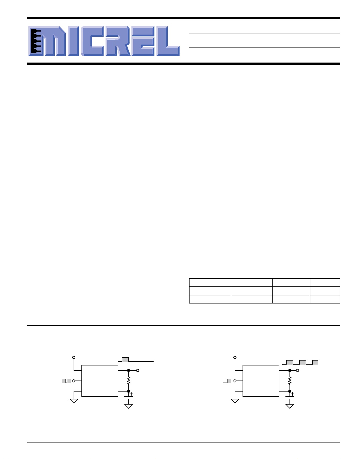
8kHz
Enabled
Disabled
VS
CS
MIC1557
4
3
GND
2
+5V
OUT
5
T/T
1
Output
1k
0.1µF
MIC1555/1557
IttyBitty™ RC Timer / Oscillator
General Description
The MIC1555 IttyBitty™ CMOS RC timer/oscillator and
MIC1557 IttyBitty CMOS RC oscillator are designed to provide rail-to-rail pulses for precise time delay or frequency
generation.
The devices are similar in function to the industry standard
“555”, without a frequency control (FC) pin or an opencollector discharge (D) pin. The threshold pin (TH) has
precedence over the trigger (TR) input, ensuring that the
BiCMOS output is off when TR is high.
The MIC1555 may be used as an astable (oscillator) or
monostable (one-shot) with separate threshold and trigger
inputs. In the one-shot mode, the output pulse width is
precisely controlled by an external resistor and a capacitor.
Time delays may be accurately controlled from microseconds to hours. In the oscillator mode, the output is used to
provide precise feedback, with a minimum of one resistor and
one capacitor producing a 50% duty cycle square wave.
The MIC1557 is designed for astable (oscillator) operation
only, with a chip select/reset (CS) input for low power shutdown. One resistor and one capacitor provide a 50% duty
cycle square wave. Other duty-cycle ratios may be produced
using two diodes and two resistors.
The MIC1555/7 is powered from a +2.7V to +18V supply
voltage.
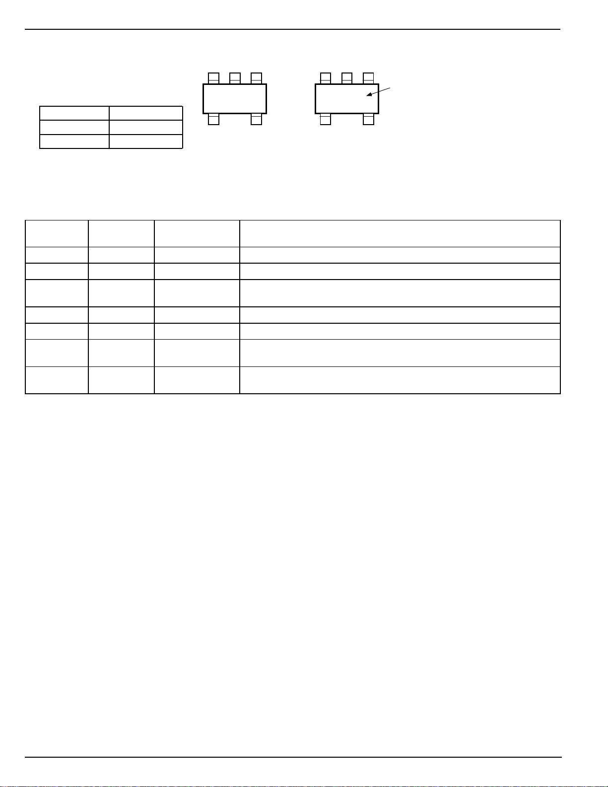
The MIC1555/7 is available in the SOT-23-5 5-lead package,
and is rated for –40°C to +85°C ambient temperature range.
Features
• +2.7V to +18V operation
• Low current
<1µA typical shutdown mode (MIC1557)
200µA typical (TRG and THR low) at 3V supply
• Timing from microseconds to hours
• “Zero” leakage trigger and threshold inputs
• 50% square wave with one Resistor, one Capacitor
• Threshold input precedence over trigger input
• <15Ω output on resistance
• No output cross-conduction current spikes
• <0.005%/°C temperature stability
• <0.055%/V supply stability
• Small SOT-23-5 surface mount package
Applications
• Precision timer
• Pulse generation
• Sequential timing
• Time-delay generation
• Missing pulse detector
• Micropower oscillator to 5MHz
• Charge-pump driver
• LED blinker
• Voltage converter
• Linear sweep generator
• Variable frequency and duty cycle oscillator
• Isolated feedback for power supplies
Ordering Information
Part Number Temp. Range Package Marking
MIC1555BM5 –40°C to +85°C SOT-23-5 T10
MIC1557BM5 –40°C to +85°C SOT-23-5 T11
Typical Applications
+5V
MIC1555
13
VS OUT
Standby
Trigger
October 1998 1 MIC1555/1557
4
TRG
GND2THR
Monostable (One-Shot)
100µs
Output
1k
5
0.1µF
Astable (Oscillator)
Page 2
MIC1555/1557 Micrel
Pin Configuration
VS
GND GND
13
22
CS
T10
45
THRTRG
T11
T/T
13
Part
Identification
OUTVS
Part Number Identification
MIC1555BM5 T10
OUT
45
MIC1557BM5 T11
SOT-23-5 (M5)
Pin Description
Pin Number Pin Number Pin Name Pin Function
MIC1555 MIC1557
1 4 VS Supply (Input): +2.7 to +18V supply.
2 2 GND Ground: Supply return.
>2
3 CS Chip Select/Reset (Input): Active high at
<1⁄3VS.
3 5 OUT Output: CMOS totem-pole output.
4 TRG Trigger (Input): Sets output high. Active low (at ≤ 2⁄3VS nominal)
5 THR Threshold (Dominant Input): Sets output low. Active high (at ≥ 2⁄3V
nominal).
1 T/T Trigger/Threshold (Input): Internally connected to both threshold and trigger
functions. See TRG and THR.
⁄3VS. Output off when low at
.
S
MIC1555/1557 2 October 1998
Page 3

MIC1555/1557 Micrel
Absolute Maximum Ratings
Supply Voltage (VS) ....................................................+22V
Threshold Voltage (V
Trigger Voltage (V
Lead Temperature (soldering 10sec.) ....................... 300°C
TRG
, V
THR
, V
) ..................................+22V
T/T
) .......................................+22V
T/T
Operating Ratings
Supply Voltage (VS) ..................................... +2.7V to +18V
Ambient Temperature Range (TA) ............. –40°C to +85°C
Package Thermal Resistance
(θJA)...................................................................220°C/W
(θJC) ..................................................................130°C/W
Electrical Characteristics
TA = 25°C, bold values indicate –40°C ≤ TA ≤ +85°C; unless noted.
Parameter Condition Min Typ Max Units
Supply current VS = 5V 240 300 µA
VS = 15V 350 400 µA
Monostable Timing Accuracy RA = 10k, C =0.1µF, VS = 5V 2 %
RA = 10k, C =0.1µF, VS = 5V 858 1161 µs
Monostable Drift over Temp VS = 5V, –55 ≤ TA ≤ +125°C, Note 1 100 ppm/°C
VS =10V, –55 ≤ TA ≤ +125°C, Note 1 150 ppm/°C
VS = 15V, –55 ≤ TA ≤ +125°C, Note 1 200 ppm/°C
Monostable Drift over Supply VS = 5V to 15V, Note 1 0.5 %/V
Astable Timing Accuracy RA = RB = 10k, C = 0.1µF, VS = 5V 2 %
RA = RB = 10k, C = 0.1µF, VS = 5V 1717 2323 µs
Maximum Astable Frequency RT = 1k, CT = 47pF, Vs = 8V 5 MHz
Astable Drift over Temp VS = 5V, –55 ≤ TA ≤ +125°C, Note 1 100 ppm/°C
VS =10V, –55 ≤ TA ≤ +125°C, Note 1 150 ppm/°C
VS = 15V, –55 ≤ TA ≤ +125°C, Note 1 200 ppm/°C
Astable Drift over Supply VS = 5V to 15V, Note 1 0.5 %/V
Threshold Voltage VS = 15V 61 67 72 %V
Trigger Voltage VS = 15V 27 32 37 %V
Trigger Current VS = 15V 50 nA
Threshold Current VS = 15V 50 nA
Chip Select on > 2/3V
off < 1/3V
Output Voltage Drop VS = 15V, I
VS = 5V, I
Output Voltage Drop VS = 15V, I
VS = 5V, I
Supply Voltage functional operation, Note 1 2.7 18 V
Output Rise Time RL = 10M, CL = 10pF, VS = 5V, Note 1 15 ns
Output Fall Time RL = 10M, CL = 10pF, VS = 5V, Note 1 15 ns
S
S
= 20mA 0.3 1.25 V
SINK
= 3.2mA 0.08 0.5 V
SINK
SOURCE
SOURCE
= 20mA 14.1 14.7 V
= 3.2mA 3.8 4.7 V
50 67 72 %V
28 33 50 %V
S
S
S
S
General Note: Devices are ESD protected, however handling precautions are recommended.
Note 1: Not tested.
October 1998 3 MIC1555/1557
Page 4

MIC1555/1557 Micrel
Typical Characteristics (T
Astable Frequency
100
10
1
100k
0.1
0.01
CAPACITANCE (µF)
0.001
0.0001
1M
-1
1x1001x1011x1021x1031x1041x1051x1061x10
1x10-21x10
FREQUENCY (Hz)
On Resistance
vs. Temperature
70
60
50
40
30
20
ON RESISTANCE (Ω)
10
0
-40 -20 0 20 40 60 80 100
TEMPERATURE (°C)
RT=1k
10k
= 25°C, VIN = +5)
A
7
Pulse Width
RT=1k
10k
-1
1x1001x1011x1021x1031x1041x1051x1061x10
1x10
PERIOD (µs)
CAPACITANCE (µF)
0.001
0.0001
100
10
1
0.1
0.01
Supply Current
vs. Temperature
-40 -20 0 20 40 60 80 100
TEMPERATURE (°C)
SUPPLY CURRENT (µA)
300
280
260
240
220
200
1M
100k
On Resistance
vs. Supply Voltage
70
60
50
40
30
20
ON RESISTANCE (Ω)
10
7
0
0 5 10 15 20
SUPPLY VOLTAGE (V)
Supply Current
vs. Supply Voltage
500
400
300
200
100
SUPPLY CURRENT (µA)
0
0 5 10 15 20
SUPPLY VOLTAGE (V)
k Factors
2.0
1.9
1.8
1.7
1.6
1.5
1.4
k FACTOR
1.3
1.2
1.1
1.0
10 100 1000
Times RC
t=k2 RC
RC (µs)
f=1⁄k
1
MIC1557 Chip Select
vs. Supply Voltage
14
12
10
8
6
4
2
CHIP SELECT VOLTAGE (V)
0
ON
OFF
3 6 9 12 15 18
SUPPLY VOLTAGE (V)
RC
MIC1555/1557 4 October 1998
Page 5

MIC1555/1557 Micrel
S
R
Q
T/T
OUT
VS
Bias
GND
CS
V
SUPPLY
MIC1557
Output
1k
0.1µF
8kHz
1M
Functional Diagrams
V
SUPPLY
VS
MIC1555
Bias
THR
100µs
OUT
1k
Standby
Trigger
<100µs
S
Q
R
TRG
GND
MIC1555 Block Diagram with External Components
(Monostable Configuration)
Functional Description
Refer to the block diagrams.
The MIC1555/7 provides the logic for creating simple RC
timer or oscillator circuits.
The MIC1555 has separate THR (threshold) and TRG
(trigger) connections for monostable (one-shot) or astable
(oscillator) operation.
The MIC1557 has a single T/T (threshold and trigger) connection for astable (oscillator) operation only. The MIC1557
includes a CS (chip select/reset) control.
Supply
VS (supply) is rated for +2.7V to +18V. An external capacitor
is recommended to decouple noise.
Resistive Divider
The resistive voltage divider is constructed of three equal
value resistors to produce 1⁄3VS and 2⁄3VS voltage for trigger
and threshold reference voltages.
Chip Select/Reset (MIC1557 only)
CS (chip select/reset) controls the bias supply to the oscillator’s
internal circuitry. CS must be connected to CMOS logic-high
or logic-low levels. Floating CS will result in unpredictable
operation. When the chip is deselected, the supply current is
less than 1µA. Forcing CS low resets the MIC1557 by setting
the flip flop, forcing the output low.
Threshold Comparator
The threshold comparator is connected to S (set) on the RS
flip-flop. When the threshold voltage (2⁄3VS) is reached, the
flip-flop is set, making the output low. THR is dominant over
TRG.
Output
0.1µF
MIC1557 Block Diagram with External Components
(Astable Configuration)
Trigger Comparator
The trigger comparator is connected to R (reset) on the RS
flip-flop. When TRG (trigger) goes below the trigger voltage
(1⁄3VS), the flip-flop resets, making the output high.
Flip-Flop and Output
A reset signal causes Q to go low, turning on the P-channel
MOSFET and turning off the N-channel MOSFET. This
makes the output rise to nearly VS.
A set signal causes Q to go high, turning off the P-channel
MOSFET, and turning on the N-channel MOSFET, grounding
OUT.
Basic Monostable Operation
Refer to the MIC1555 functional diagram.
A momentary low signal applied to TRG causes the output to
go high. The external capacitor charges slowly through the
external resistor. When V
(threshold voltage) reaches 2⁄3
THR
VS, the output is switched off, discharging the capacitor.
During power-on, a single pulse may be generated.
Basic Astable Operation
Refer to the MIC1557 functional diagram.
The MIC1557 starts with T/T low, causing the output to go
high. The external capacitor charges slowly through the
external resistor. When V
reaches 2⁄3VS (threshold volt-
T/T
age), the output is switched off, slowly discharging the
capacitor. When V
output is switched on, causing V
decreases to 1⁄3VS (trigger voltage), the
T/T
to rise again, repeating
T/T
the cycle.
October 1998 5 MIC1555/1557
Page 6

MIC1555/1557 Micrel
Application Information
Basic Monostable (One-Shot) Circuit
A monostable oscillator produces a single pulse each time
that it is triggered, and is often referred to as a “one-shot”. The
pulse width is constant, while the time between pulses
depends on the trigger input. One-shots are generally used
to “stretch” incoming pulses, of varying widths, to a fixed
width. The IttyBitty MIC1555 is designed for monostable
operation, but may also be connected to provide astable
oscillations. The pulse width is determined by the time it takes
to charge a capacitor from ground to a comparator trip point.
If the capacitor (CT) is charged through a resistor (RT)
connected to the output of an MIC1555, the trip point is
approximately 1.1RCT (the same time as the initial power-on
cycle of an astable circuit.) If the trigger pulse of an MIC1555
remains low longer than the output pulse width, short oscillations may be seen in the output of a one-shot circuit, since the
threshold pin has precedence over the trigger pin. These
occur since the output goes low when the threshold is
exceeded, and then goes high again as the trigger function is
asserted. AC coupling the input with a series capacitor and
a pull-up resistor, with an RC time constant less than the
pulse width, will prevent these short oscillations. A diode (DT)
in parallel with (RT) resets the one-shot quickly.
2.7V to 18V
R
T
D
T
R
PU
THR
5
C
Trigger
1
⁄3V
IN
IN
TRG
4
C
T
MIC1555
Figure 1. One-Shot Diagram
The period of a monostable circuit is:
t = k2 RC
where:
t = period (s)
k2 = constant [from Typical Characteristics graph]
R = resistance (Ω)
C = capacitance (F)
Basic Astable (Oscillator) Circuits
An astable oscillator switches between two states, “on” and
“off”, producing a continuous square wave. The IttyBitty
MIC1557 is optimized for this function, with the two comparator inputs, threshold and trigger (T/T), tied together internally.
Chip select (CS) is brought out to allow on-off control of the
oscillator.
VS
GND
CS
OUT
1
tON = 1.1RTC
OUT
3
2
T
The MIC1555 may also be used as an astable oscillator by
tying the threshold and trigger pins together, forming a T/T
pin. If a resistor (RT) is connected from the output to a
grounded timing capacitor, (CT) the voltage at their junction
will ramp up from ground when the output goes high. If the T/
T pin is connected to this junction, the output will switch low
when the ramp exceeds 2⁄3 of the input voltage. The junction's
voltage ramps down toward ground while the output is low.
When the ramp is below 1⁄3 of the input voltage, the output
switches to high, and the junction ramps up again.
The continuing frequency of an MIC1555/7 astable oscillator
depends on the RC time constant, and is approximately 0.7/
RC below 1MHz. At frequencies above 1MHz the RC
multiplier increases as capacitance is decreased, and propagation delay becomes dominant. Non-symmetrical oscillator
operation is possible at frequencies up to 5MHz.
If a duty cycle other than 50% is desired, a low-power signal
diode may be connected in series with the timing resistor
(RA), and a second resistor (RB) in series with an opposite
facing diode connected in parallel. The frequency is then
made up of two components, the charging time (tA) and the
discharging time (tB) tA= 0.7RAC and tB= 0.7RBC. The
frequency is the reciprocal of the sum of the two times tA + tB,
so the total time is 1.4RTCT. The first half-cycle of an astable,
after power-on or CS enable, is lengthened since the capacitor is charging from ground instead of the 1⁄3 input trigger trip
voltage, to 1.1RC, the same as a monostable pulse.
2.7V to 18V
C
B
4
VS
R
E
T/T
1
MIC1557
1k to 1M
C
T
100pF to 10µF
GND
R
A
R
B
CS
OUT
CS
3
OUT
5
2
t
t = 0.7(RA+RB)C
T
Figure 2. Oscillator Diagram
The MIC1555 or MIC1557 can be used to construct an
oscillator.
The frequency of an astable oscillator is:
1
f
=
k RC
1
where:
f = frequency (Hz)
k1 = constant [from Typical Characteristics graph]
R = resistance (Ω)
C = capacitance (F)
MIC1555/1557 6 October 1998
Page 7

MIC1555/1557 Micrel
THR
OUT
MIC1555
1
3
GND
2
VS
5
TRG
4
+5V +12V
R
L
OFF ≥ 3.3V
ON ≤ 1.6V
To use the MIC1555 as an oscillator, connect TRG to THR.
+5V
1
4
2
MIC1555
VS
TRG
GND
OUT
THR
8kHz
3
5
Output
1k
0.1µF
Figure 3. MIC1555 Oscillator Configuration
The MIC1557 features a CS input. When logic-low, CS
places the MIC1557 into a <1µA shutdown state. If unused,
the MIC1557 CS input on must be pulled up.
+5V
1M
4
3
2
MIC1557
VS
CS
GND
OUT
T/T
8kHz
5
Output
1k
1
0.1µF
Figure 4. MIC1557 Oscillator Configuration
Falling-Edge Triggered Monostable Circuit
The MIC1555 may be triggered by an ac-coupled fallingedge, as shown in figure 5. The RC time constant of the
input capacitor and pull-up resistor should be less than the
output pulse time, to prevent multiple output pulses. A
diode across the timing resistor provides a fast reset at the
end of the positive timing pulse.
Input
+5V
1M
MIC1555
13
VS OUT
4
TRG
GND2THR
100µs
Output
1N41481k
5
0.1µF
Accuracy
The two comparators in the MIC1555/7 use a resistor voltage
divider to set the threshold and trigger trip points to approximately 2⁄3 and 1⁄3 of the input voltage, respectively. Since the
charge and discharge rates of an RC circuit are dependent on
the applied voltage, the timing remains constant if the input
voltage varies. If a duty cycle of exactly 50% (or any other
value from 1 to 99%), two resistors (or a variable resistor) and
two diodes are needed to vary the charge and discharge
times. The forward voltage of diodes varies with temperature,
so some change in frequency will be seen with temperature
extremes, but the duty cycle should track. For absolute timing
accuracy, the MIC1555/7 output could be used to control
constant current sources to linearly charge and discharge the
capacitor, at the expense of added components and board
space.
Long Time Delays
Timing resistors larger than 1MΩ or capacitors larger than
10µF are not recommended due to leakage current inaccuracies. Time delays greater than 10 seconds are more accurately produced by dividing the output of an oscillator by a
chain of flip-flop counter stages. To produce an accurate
one-hour delay, for example, divide an 4.55Hz MIC1557
oscillator by 16,384 (4000
, 214) using a CD4020 CMOS
hex
divider. 4.5Hz may be generated with a 1µF CT and approximately 156kΩ.
Inverting Schmitt Trigger
Refer to figure 7. The trip points of the MIC1555/7 are defined
as 1/3 and 2/3VS, which allows either device to be used as a
signal conditioning inverter, with hysteresis. A slowly changing input on T/T will be converted to a fast rise or fall-time
opposite direction rail-to-rail output voltage. This output may
be used to directly drive the gate of a logic-level P-channel
MOSFET with a gate pull-up resistor. This is an inverted logic
low-side logic level MOSFET driver. A standard N-channel
MOSFET may be driven by a second MIC1555/7, powered by
12V to 15V, to level-shift the input.
Figure 5. Falling-Edge Trigger Configuration
Rising-Edge Triggered Monostable Circuit
The MIC1555 may be triggered by an ac-coupled risingedge, as shown in figure 6. The pulse begins when the accoupled input rises, and a diode from the output holds the
THR input low until TRG discharges to 1⁄3VS. This circuit
provides a low-going output pulse.
+5V
MIC1555
13
VS OUT
4
TRG
GND2THR
5
Figure 6. Rising-Edge Trigger Configuration
October 1998 7 MIC1555/1557
0.1µF
1N41481k
100µs
Output
Input
Figure 7. Schmitt trigger
Charge-Pump Low-Side MOSFET Drivers
A standard MOSFET requires approximately 15V to fully
enhance the gate for minimum R
. Substituting a logic-
DS(on)
level MOSFET reduces the required gate voltage, allowing
an MIC1557 to be used as an inverting Schmitt Trigger,
described above. An MIC1557 may be configured as a
voltage quadrupler to boost a 5V input to over 15V to fully
enhance an N-channel MOSFET which may have its drain
Page 8

MIC1555/1557 Micrel
connected to a higher voltage, through a high-side load. A
TTL high signal applied to CS enables a 10kHz oscillator,
which quickly develops 15V at the gate of the MOSFET,
clamped by a zener diode. A resistor from the gate to ground
ensures that the FET will turn off quickly when the MIC1557
is turned off.
+12V
C1
100pF
to 10µF
TTL High = ON
+5V
MIC1557
43
VS
1
T/T
2
GND
RT 1k to 1M
CS
OUT
5
R
E
100k
N-Channel
MOSFET
(IRF540)
15V
R
Figure 8. Charge-Pump
Audible Voltmeter
If an additional charge or discharge source is connected to
the timing capacitor, the frequency may be shifted by turning
the source on or off. An MIC1555 oscillator, powered by the
circuit under test, may be used to drive a small loudspeaker
or piezo-electric transducer to provide a medium frequency
for an open or high impedance state at the probe. A high tone
is generated for a high level, and a lower frequency for a logic
L
low on the probe.
+5V to +18VRT 10k
1N914
10k
47k
C
T
0.01µF
5
4
2
MIC1555
THR
TRG
GND
VS
OUT
1
3
0.001µF
10k
Figure 9. Audible Voltmeter
100Ω
Package Information
1.90 (0.075) REF
0.95 (0.037) REF
3.02 (0.119)
2.80 (0.110)
0.50 (0.020)
0.35 (0.014)
1.75 (0.069)
1.50 (0.059)
1.30 (0.051)
0.90 (0.035)
0.15 (0.006)
0.00 (0.000)
SOT-23-5 (M5)
3.00 (0.118)
2.60 (0.102)
10°
0°
DIMENSIONS:
MM (INCH)
0.20 (0.008)
0.09 (0.004)
0.60 (0.024)
0.10 (0.004)
MICREL INC. 1849 FORTUNE DRIVE SAN JOSE, CA 95131 USA
TEL + 1 (408) 944-0800 FAX + 1 (408) 944-0970 WEB http://www.micrel.com
This information is believed to be accurate and reliable, however no responsibility is assumed by Micrel for its use nor for any infringement of patents or
other rights of third parties resulting from its use. No license is granted by implication or otherwise under any patent or patent right of Micrel Inc.
© 1998 Micrel Incorporated
MIC1555/1557 8 October 1998
 Loading...