

Page 1
P-Channel 20V (D-S)MOSFET
MI2303
General Description
This miniature surface monut MOSFET u ses
advanced trench process, lo w RDS(on) a ssu res
minimal po wer loss and energy c onv ers ion ,which
ma kes th is de vice i deal f or us e in po wer
management circuit.
Applications
Load switch
DC-D C con ver ter s
Power management
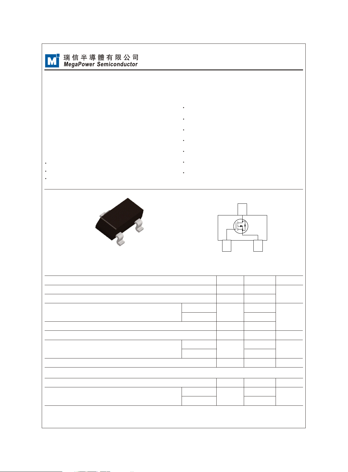
D
S
G
SOT23
Features
VD S (V) = -20V
ID (A) = -3.3A (VG S = -4. 5V)
RD S(on) = 8 5 mΩ @ VGS = -4.5V
RD S(on) = 9 5 mΩ @ VGS = -2. 5V
RD S(on) = 120 mΩ @ VGS = -1.8 V
Low gate charge
Fast switching speed
D
G
S
Absolute Maximum Ratings (TA = 25℃ Unless Otherwise Not ed)
Parameter
Drain-Source Voltage
Gate-Source Voltage
Continuous Drain Current
Pulsed Drain Current
Continuous Source Current (Di ode C ond uct ion )
Power Dissipation
Operating Junction and Storag e Temperature Range
a
b
a
a
TA =25℃
TA =70℃
TA =25℃
TA =70℃
Symbol
VD S
VG S
ID
ID M
IS
PD
TJ ,Tstg
Thermal Resistance Ratings
Symbol
θ
R JA
Maximum Junction-to-Ambient
www.meg apo wer .com. cn
Parameter
a
t<= 10 sec
Steady-State
1
Maximum Units
-20
±8
-3.3
-2.6
V
A
-13
-1.0
1. 4
1. 0
-55 to 150
Maximum
90
130
Feb.20 12 Re v.2.0
A
W
℃
Units
℃/W
Page 2
Ordering Information
MI2303
Device
MI2303
Device Marking
MPAS
Reel Size
7’’
Specifications (TA = 25℃ Unless Otherwise Noted)
Parameter
Static
Drain-Source Breakdown Voltage
Gate-Threshold Voltage
Gate-Body Leakage
Zero Gate Voltage Drain Current
On-State Drain Current
c
Drain-Source On-Resistance
Forward Tranconductance
c
Diode Forward Voltage
Dynamic
Input Capacitance
Output Capacitance
Reverse Tra nsf er Ca pac ita nce
c
Symbol
V( BR)D SS
VG S(th )
IG SS
ID SS
ID (on)
RD S(o n)
g
fs
VS D
Ci ss
Co ss
Cr ss
Test Conditions
VG S=0V,ID=-250uA
VD S =VGS,ID = -250 u A
VD S=0V,VGS=±12V
VDS=-20V,VGS=0V
VDS=-20V,VGS=0V,TJ=55℃
VDS=-5V,VGS=-4.5V
VGS=-4.5V,ID=-4.4A
VGS =-2. 5 V, ID=- 2.0A
VGS =-1.8 V, ID=- 1.0A
VD S=-5V,ID =-2.8A
IS =-1.0A,VGS=0 V
VD S=-10V,VGS=0 V
f=1MHz
Tape Width
8mm
Limits
Min Typ Max
-20
-0.45
-0.61
-13
35
45
60
16
-0.7
1020
191
140
Quantity
3000 units
-0.9
±100
-1
-10
50
65
75
-1.2
Units
V
nA
uA
A
mΩ
S
V
pF
Switching
Total Gate Charge
Gate Sourse Charge
Gate Drain Charge
Tur n-O n Del ay Tim e
Rise Time
Tur n-O ff Delay Time
Fall-Time
Notes: a . Sur face Moun ted on 1” x 1” FR 4 Boa rd.
b. Pulse w idt h limited b y maximum j unc tion temp erature
c. Pulse t est : PW <= 300us d uty cycle < = 2%.
www.meg apo wer .com. cn
Qg
Qg s
Qg d
td (on)
tr
td (off)
tf
RG=6ohm,VGEN=-4.5V
VG S=-4.5V,
VD S=-10V,
ID =-3.3A
VDD=-10V,
RL=10ohm
2
12
1. 7
3. 2
25
42
70
47
19
nC
40
63
ns
110
74
Feb.20 12 Re v.2.0
Page 3

Typical Electrical and Thermal Ch aracteristics
MI2303
20
VGS =- 2.5V, -3V ,- 3. 5V, -4V,- 4. 5V, -5 V
16
12
8
-ID - Dra in Curren t(A )
4
1
0
0 1 2 3 4 5
Figure 1 . On- Reg ion C haracte ristics
150
120
90
VGS =- 1.8V
60
VGS =- 2.5V
-2V
-1.5 V
20
16
12
8
-ID - Dra in Curren t(A )
4
0
0 0.5 1 1.5 2 2 .5
Tc=-55 ℃
25℃
125℃
-VGS( Volts)-VDS Dra in -to-So urc e Voltage( V)
Figure 2 . Tran sfer Char acteris tic s
150
120
90
60
ID= -2A
ID= -4.4 A
30
RD S(on ) On-R esistan ce( mΩ)
0
-VGS Ga te-to-S ource Volt age (V)
Figure 3 . On- Resi sta nce vs. Dra in Curren t and
1. 5
1. 4
1. 3
1. 2
1. 1
1. 0
0. 9
0. 8
RD S(on ) On-Resi stance
(Norma liz ed)
0. 7
0. 6
www.meg apo wer .com. cn
VG S =-4 .5V
ID =-4. 4A
-50 -2 5 0 25 50 75 100 12 5 150
Figure 5 . On- Resi sta nce Var iation wi th
Gate Volt age
TJ - Junct ion Tem peratur e( )℃
Temperat ure
VGS =- 4.5V
30
RD S(on ) On-R esistan ce( mΩ)
0
0 1 2 3 4 5
Figure 4 . On Re sistanc e vs. Gate- to-So urce
20
10
1
IS -Sour ce Cu rrent(A )
0. 1
0 0. 2 0. 4 0.6 0 .8 1.0 1. 2
Figure 6 : Sou rce-Dra in Forwar d Volt age
3
-ID - Drai n Cur rent(A)
Voltage
TJ= 125℃
TJ= 25℃
VS D Sour ce -to-Dr ain Vo ltage(V )
Feb.20 12 Re v.2.0
Page 4

Typical Electrical and Thermal Ch aracteristics
MI2303
5
VD S=- 4.5V
4
ID= -4.4 A
3
2
1
-VGS, Gat e-t o-Sour ce Vol tage(V )
0
0 1 2 3 4 5
Qg- Total Gat e Charge( nC)
Figure 7. Gat e Charge
100.0
T
=150°C
J(M ax)
T A =25°C
10.0
R
DS( ON)
100 µ s
limited
1ms
(A mps )
D
I
1.0
0.1s
10ms
1s
10s
0.1
0.1
1 1
DC
0 100
VDS (Volts)
Figure 9 : Max imum Forw ard Biase d Saf e
Operat ing Ar ea (Note d)
10
t
n
ie
n
a
e
c
ive r s
t T
e n
c
p da
e
f
e
f
d
l
E
e
ma
r
z d
0.1
e
h
T
ma i
Nor l
1
D=T on/T
T
J,P K=TA +PDM
Rθ JA=130 W℃/
.
Z
JA
θ
1800
1500
1200
Ci ss
900
600
Capaci tan ce(pF)
300
Co ss
Cr ss
0
0 4 8 12 16 20
VD S Drai n-t o-Sour ce Vol tage(V )
Figure 8 :Ca pacitan ce
40
T
30
)
W
(
r
20
e
w
o
P
T A =25°C
10
0
0.001 0.0 1 0.1
1 1
Pulse Wi dth ( s)
Figure 1 0: Si ngle Puls e Power Rat ing J unction -to-
Ambien t (No te d)
In desce ndi ng order
D=0.5, 0 .3, 0 .1, 0.05, 0 .02, 0.01 , single pu lse
P
D
T
o n
T
=150°C
J(M ax)
0 100 1000
0.01
0.00001 0.0001 0.001 0.01 0.1 1 1 0 100 1000
Pulse Wi dth ( s)
Figure 11 : Normali zed Maxim um Tra nsient Therma l Imp edance
Note d:
These te sts a re perfor med with th e device mo unt ed on 1 in FR -4 bo ard with 2o z. Copper, i n a sti ll air envi ronment w ith
T A=25 °C. The SOA cu rve provi des a s ingle pul se rating .
www.meg apo wer .com. cn
2
4
Feb.20 12 Re v.2.0
Page 5

Package Outline
SOT23_3Lead
MI2303
D
3
1 2
e
e1
T OP VIEW
E1 E
Unit: mm
S ymbol Min Nom Max
A 0.70 1.15
A1 0. 00
b 0.30 0.50
c 0.20
0.08
D 2.80 3 .10
E 2.60 3.00
E1 1. 40 1 .80
1.00
---
0.40
0.13
2.90
2.80
1.60
0.13
e 0.95 BSC
e 1 1 .90 B SC
L 0.40 REF
L 1 0.54 REF
0 º º
θ
8 º
5
A
b
A1
SIDE VIEW
Notes:
(1) All dimensions are in m ill ime ters.Angles in degre es.
(2)
Package body sizes exclude m old flash and gate burrs.
(3)
Complies with JEDEC TO-236.
www.meg apo wer .com. cn
θ
L1 L
END VIEW
Doc.SOT23_3L-071012
5
Feb.20 12 Re v.2.0
c
Page 6

 Loading...