

Page 1

MFC2000
Multifunctional Peripheral Controller 2000
Hardware Description
Doc. No. 100723A
June 21, 2000
Page 2
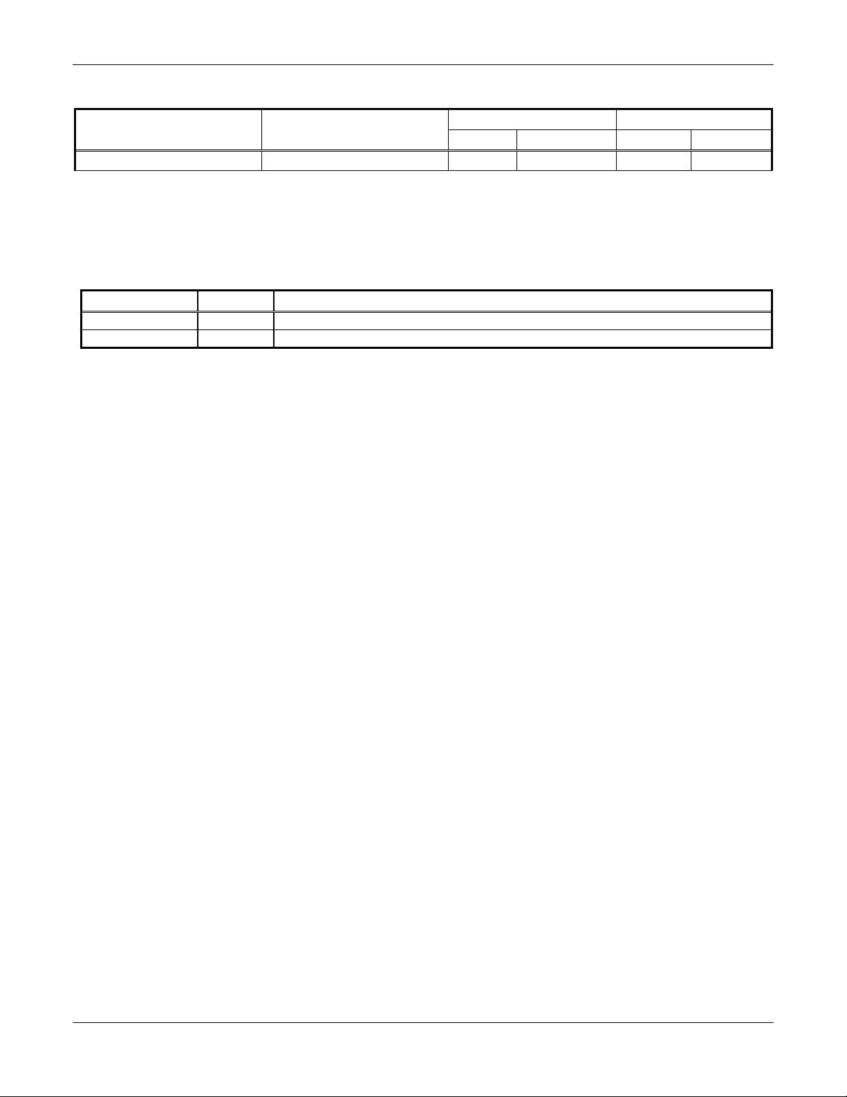
Ordering Information
Marketing Name Device Set Order No.
Part No. Package Part No. Package
MFC2000 xxx-xxx-xxx xxxxx
Revision History
Revision Date Comments
A 04/07/00 Initial, internal, preliminary release of document.
A 06/21/00 Second internal, preliminary release with revisions track ed.
© 2000, Conexant Systems, Inc. All Rights Reserved.
Information in this document is provided in connection with Conexant Systems, Inc. (" Conexant " ) products . These materials are p rovi ded by
Conexant as a service to its customers and may be used for informational purposes only. Conexant assumes no responsibili ty for errors or
omissions in these materials. Conexant may make changes to specifications and product descriptions at any time, without notice. Conexant
makes no commitment to update the information contained herein. Conexant shall have no responsibility whatsoev er for confl icts or
incompatibilities arising from future changes to its specificati ons and product descriptions.
No license, express or implied, by estoppel or otherwise, to any intellect ual property ri ghts is grant ed by this document. Except as provided in
Conexant’s Terms and Conditions of Sale for such products, Conexant assumes no liability whatsoever.
THESE MATERIALS AR E PR OVIDED "AS IS" WITHOUT W AR R AN TY OF ANY KIND, EITHER EX PR ESS OR IMPLIED, RELA TIN G TO
SALE AND/OR USE OF CONEXANT PRODUCTS INCLUDING LIABI LITY OR WARRANTIE S RE LAT ING TO FITNESS FOR A
PARTICULAR PURPOSE, MERCHANTABILITY, OR INFRINGEMENT OF ANY PATENT, COPYRIGHT OR OTHER INTELLECTUAL
PROPERTY RIGHT. Conexant further does not warrant the accuracy or completeness of the information, text, graphics or other items
contained within these materials. Conexant shall not be liable for any special, indirect, i ncidental, or consequential damages, including without
limitation, lost revenues or lost profits, which may result from the use of these materials .
Conexant products are not intended for use in medical, life saving or life sustaining applicati ons. Conexant cust om ers usi ng or selling
Conexant products for use in such applications do so at their own risk and agree to fully indemnify Conexant for any damages resulting from
such improper use or sale.
The following are trademarks of Conexant Systems, Inc.: Conexant, the Conexant C symbol, “What’s Next in Communic ations Technologies”,
and SmartDAA. Product names or services listed in this publication are for identification purpos es only, and may be trademarks of third
parties. Third-party brands and names are the property of their respective owners.
Reader Response:
Conexant strives to produce quality documentation and welcomes your feedback. Please send comments
and suggestions to conexant.tech.pubs@conexant.com. For technical questions, contact your local Conexant sales office or
field applications engineer.
ii
Conexant
100723A
Page 3

Contents
1. INTRODUCTION..............................................................................................................................................1-1
1.1 SCOPE ......................................................................................................................................................1-1
1.2 SYSTEM OVERVIEW................................................................................................................................1-1
1.3 REFERENCE DOCUMENTATION............................................................................................................ 1-5
2. MFC2000 SUMMARY ...................................................................................................................................... 2-1
2.1 MFC2000 DEVICE FAMILY....................................................................................................................... 2-1
2.2 MFC2000 SYSTEM BLOCK DIAGRAM .................................................................................................... 2-1
3. HARDWARE INTERFACE............................................................................................................................... 3-1
3.1 PIN DESCRIPTION ...................................................................................................................................3-1
3.2 MAXIMUM RATINGS.................................................................................................................................3-7
3.3 ELECTRICAL CHARACTERISTICS..........................................................................................................3-8
3.4 PIN LAYOUT............................................................................................................................................3-10
4. CPU AND BUS INTERFACE...........................................................................................................................4-1
4.1 MEMORY MAP AND CHIP SELECT DESCRIPTION...............................................................................4-1
4.2 CACHE MEMORY CONTROLLER..........................................................................................................4-19
4.3 SIU………. ...............................................................................................................................................4-24
4.4 INTERRUPT CONTROLLER................................................................................................................... 4-46
4.5 DRAM CONTROLLER (INCLUDING BATTERY DRAM)........................................................................4-54
4.6 FLASH MEMORY CONTROLLER...........................................................................................................4-72
4.7 DMA CONTROLLER ...............................................................................................................................4-76
5. RESET LOGIC/BATTERY BACKUP/WATCH DOG TIMER...........................................................................5-1
5.1 RESET LOGIC/BATTERY BACKUP ......................................................................................................... 5-1
5.2 WATCHDOG TIMER ...............................................................................................................................5-11
6. FAX TIMING CONTROL INTERFACE............................................................................................................6-1
6.1 PLL………….. ............................................................................................................................................6-1
6.2 FAX TIMING LOGIC ..................................................................................................................................6-2
6.3 MFC2000 TIMING CHAIN .........................................................................................................................6-3
6.4 SCAN CONTROL TIMING......................................................................................................................... 6-4
6.5 FAX TIMING REGISTERS.........................................................................................................................6-5
7. VIDEO/SCANNER CONTROLLER .................................................................................................................7-1
7.1 SCANNER CONTROLLER........................................................................................................................ 7-2
7.2 SERIAL PROGRAMMING INTERFACE..................................................................................................7-41
7.3 VIDEO CONTROLLER ............................................................................................................................7-50
8. ADC……...........................................................................................................................................................8-1
8.1 PADC AND SCAN ANALOG FRONT END ...............................................................................................8-1
8.2 TADC……………………. ........................................................................................................................... 8-5
100723A
Conexant
iii
Page 4

9. BI-LEVEL RESOLUTION CONVERSION ....................................................................................................... 9-1
9.1 FUNCTIONAL DESCRIPTION .................................................................................................................. 9-1
9.2 REGISTER DESCRIPTION....................................................................................................................... 9-6
9.3 RESOLUTION CONVERSION PROGRAMMING EXAMPLES............................................................... 9-15
10. EXTERNAL PRINT ASIC INTERF ACE.........................................................................................................10-1
10.1 INTERFACE BETWEEN THE MFC2000 AND EXTERNAL PRINT ASIC..........................................10-1
11. BIT ROTATION LOGIC.................................................................................................................................. 11-1
11.1 FUNCTIONAL DESCRIPTION............................................................................................................11-1
11.2 BLOCK DIAGRAM...............................................................................................................................11-3
11.3 REGISTER DESCRIPTION.................................................................................................................11-6
11.4 FIRMWARE OPERATION................................................................................................................. 11-10
12. PRINTER AND SCANNER STEPPER MOTOR INTERFACE...................................................................... 12-1
12.1 VERTICAL PRINT STEPPER MOTOR INTERFACE .........................................................................12-1
12.2 SCANNER STEPPER MOTOR INTERFACE.....................................................................................12-5
13. GENERAL PURPOSE INPUTS/OUTPUTS (GPIO) ...................................................................................... 13-1
13.1 GPIO SIGNALS...................................................................................................................................13-1
13.2 GPO/GPI SIGNALS............................................................................................................................. 13-5
13.3 GPIO CONTROL AND DATA REGISTERS........................................................................................13-6
14. COMPRESSOR AND DECOMPRESSOR..................................................................................................... 14-1
14.1 FUNCTIONAL DESCRIPTION............................................................................................................14-1
14.2 REGISTER DESCRIPTION.................................................................................................................14-2
15. SYNCHRONOUS/ASYNCHRONOUS SERIAL INTERFACE (SASIF).........................................................15-1
15.1 FUNCTIONAL DESCRIPTION............................................................................................................15-1
15.2 REGISTER DESCRIPTION.................................................................................................................15-3
15.3 SASIF TIMING...................................................................................................................................15-12
15.4 FIRMWARE OPERATION.................................................................................................................15-16
16. USB INTERFACE .......................................................................................................................................... 16-1
16.1 FUNCTION DESCRIPTION ................................................................................................................ 16-1
16.2 REGISTER DESCRIPTION.................................................................................................................16-1
16.3 FIRMWARE OPERATION.................................................................................................................16-23
17. BI-DIRECTIONAL PARALLEL PERIPHERAL INTERFACE........................................................................ 17-1
17.1 OPERATIONAL MODES..................................................................................................................... 17-1
17.2 ADDITIONAL FEATURES................................................................................................................... 17-2
17.3 FUNCTIONAL DESCRIPTION............................................................................................................17-3
17.4 REGISTER DESCRIPTION.................................................................................................................17-4
17.5 TIMING..............................................................................................................................................17-16
17.6 FIRMWARE OPERATION.................................................................................................................17-22
iv
Conexant
100723A
Page 5

18. REAL-TIME CLOCK ...................................................................................................................................... 18-1
18.1 DESCRIPTION....................................................................................................................................18-1
18.2 REAL-TIME CLOCK (RTC) REGISTERS ...........................................................................................18-2
18.3 RTC OPERATIONS.............................................................................................................................18-3
19. SYNCHRONOUS SERIAL INTERFACE (SSIF)............................................................................................19-1
19.1 INTRODUCTION AND FEATURES....................................................................................................19-1
19.2 REGISTER DESCRIPTION.................................................................................................................19-2
19.3 SSIF TIMING.......................................................................................................................................19-7
20. PROGRAMMABLE TONE GENERATORS ..................................................................................................20-1
20.1 INTRODUCTION.................................................................................................................................20-1
20.2 BELL/RINGER GENERATOR.............................................................................................................20-1
20.3 TONE GENERATOR........................................................................................................................... 20-6
21. PWM LOGIC .................................................................................................................................................. 21-1
21.1 FUNCTIONAL DESCRIPTION............................................................................................................21-1
21.2 REGISTER DESCRIPTION.................................................................................................................21-2
22. CALLING PARTY CONTROL (CPC) ............................................................................................................22-1
22.1 REGISTERS DESCRIPTION..............................................................................................................22-5
23. SSD_P80........................................................................................................................................................23-1
23.1 FUNCTION DESCRIPTION ................................................................................................................ 23-1
23.2 REGISTER DESCRIPTION.................................................................................................................23-3
23.3 FIRMWARE OPERATION...................................................................................................................23-6
24. COUNTACH IMAGING DSP BUS SUBSYSTEM ......................................................................................... 24-1
24.1 COUNTACH IMAGING DSP SUBSYSTEM........................................................................................ 24-3
24.2 COUNTACH IMAGING DSP BUS UNIT ............................................................................................. 24-4
24.3 ARM BUS INTERFACE.......................................................................................................................24-8
24.4 COUNTACH IMAGING DSP SUBSYSTEM INTERFACE ................................................................24-11
24.5 COUNTACH DMA CONTROLLER.................................................................................................... 24-12
24.6 VIDEO/SCANNER INTERFACE ....................................................................................................... 24-22
24.7 (S)DRAM CONTROLLER ((S)DRAMC)............................................................................................24-23
24.8 REGISTER DESCRIPTION...............................................................................................................24-28
25. CONFIGURATION ......................................................................................................................................... 25-1
25.1 HARDWARE VERSION ......................................................................................................................25-1
25.2 PRODUCT CODE ............................................................................................................................... 25-1
100723A
Conexant
v
Page 6

Figures
Figure 1-1. MFP System Diagram Using MFC2000 .............................................................................................................. 1-1
Figure 1-2: MFC2000 Function Diagram............................................................................................................................... 1-4
Figure 2-1.
Figure 3-1. MFC2000 BGA Bottom View............................................................................................................................. 3-10
Figure 4-1. MFC2000 Memory Map....................................................................................................................................... 4-6
Figure 4-2. MFC2000 Internal Memory Map.......................................................................................................................... 4-7
Figure 4-3. MFC2000 Cache Organization.......................................................................................................................... 4-19
Figure 4-4. 2-Way Interleave ROM Connection................................................................................................................... 4-26
Figure 4-5. Zero Wait State, Single Access, Normal Read, Normal Write........................................................................... 4-36
Figure 4-6. One Wait State, Single Access, One Read, One Write..................................................................................... 4-37
Figure 4-7. Two Wait States, Single Access, Read On Delayed (CS1n), Write Early Off (CS2n)........................................ 4-38
Figure 4-8. Zero Wait State, Burst Access, Normal Read, Normal Write............................................................................. 4-39
Figure 4-9. Fast Page Mode ROM Access1,0,0 Read Access Followed by 1,1,1,1, Write Access.................................. 4-40
Figure 4-10. System Bus TimingRead/Write with Wait States ......................................................................................... 4-41
Figure 4-11. System Bus TimingZero-Wait-State Read/Write.......................................................................................... 4-42
Figure 4-12. System Bus Timing2-Way Interleave Read Timing (S = 1).......................................................................... 4-43
Figure 4-13. System Bus Timing2-Way Interleave Write Timing (S = 0 or 1)................................................................... 4-44
Figure 4-14. External Interrupt Request Timing................................................................................................................... 4-54
Figure 4-15. DRAM Bank/Address Map............................................................................................................................... 4-56
Figure 4-16. Simplified DRAM Controller Block Diagram .................................................................................................... 4-59
Figure 4-17. DRAM Interface Example................................................................................................................................ 4-60
Figure 4-18. 8-bit Memory Data Bus....................................................................................................................................4-65
Figure 4-19. 16-bit Memory Data Bus.................................................................................................................................. 4-65
Figure 4-20. CASn Non-Interleaved 8-bit DRAM Read........................................................................................................4-66
Figure 4-21. 2-Way Interleaved Memory with Halfword Bursts of Data............................................................................... 4-66
Figure 4-22. 2-Way Interleaved DRAM Read (3 words)...................................................................................................... 4-67
Figure 4-23. 2-Way Interleaved DRAM Write ...................................................................................................................... 4-67
Figure 4-24. Refresh Cycle.................................................................................................................................................. 4-68
Figure 4-25. DRAM TimingRead, Write and Wait States for Non-interleave Mode.......................................................... 4-68
Figure 4-26. DRAM Timing for 2-way Interleave Write........................................................................................................ 4-69
Figure 4-27. DRAM TimingRead for 2-way interleave mode............................................................................................ 4-69
Figure 4-28. DRAM Refresh Timing.................................................................................................................................... 4-70
Figure 4-29. DRAM Battery Refresh Timing........................................................................................................................ 4-70
Figure 4-30. Flash Control Block Diagram........................................................................................................................... 4-73
Figure 4-31. NAND-Type Flash Memory Access with Two Wait States .............................................................................. 4-75
Figure 4-32: External DMA Read Timing (Single Access, One Wait State) ....................................................................... .. 4-80
Figure 4-33. External DMA Write Timing (Single Access, One Wait State).........................................................................4-81
Figure 4-34. USB Logical Channels Block Diagram............................................................................................................ 4-82
Figure 5-1. Power Reset Block Diagram................................................................................................................................ 5-2
MFC2000 Organization
....................................................................................................................................... 2-2
vi
Conexant
100723A
Page 7

Figure 5-2. Power-down Select Logic.................................................................................................................................... 5-3
Figure 5-3. Power Reset Timing Diagram.............................................................................................................................. 5-5
Figure 5-4. +5v Prime Power Signal and VGG...................................................................................................................... 5-6
Figure 5-5. Internal Power Detection................................................................................................................................... 5-10
Figure 5-6. Figure Caption Required................................................................................................................................... 5-10
Figure 5-7. Voltage Divider Circuit....................................................................................................................................... 5-11
Figure 5-8. Watchdog Timer Block Diagram........................................................................................................................ 5-12
Figure 5-9. Watchdog Time-Out Timing Diagram................................................................................................................ 5-13
Figure 6-1. Fax Timing Control Logic Block Diagram............................................................................................................6-2
Figure 6-2. MFC2000 Timing Chain...................................................................................................................................... 6-3
Figure 6-3. Scan Control Timing............................................................................................................................................ 6-4
Figure 7-1. Video/Scanner Controller Block Diagram............................................................................................................ 7-1
Figure 7-2. Untitled Timing Diagram.................................................................................................................................... 7-19
Figure 7-3. Untitled Timing Diagram.................................................................................................................................... 7-20
Figure 7-4. Untitled Timing Diagram.................................................................................................................................... 7-20
Figure 7-5. Untitled Timing Diagram.................................................................................................................................... 7-21
Figure 7-6. Untitled Timing Diagram.................................................................................................................................... 7-22
Figure 7-7. Untitled Timing Diagram.................................................................................................................................... 7-23
Figure 7-8. Untitled Timing Diagram.................................................................................................................................... 7-23
Figure 7-9. Untitled Timing Diagram.................................................................................................................................... 7-24
Figure 7-10. Untitled Timing Diagram.................................................................................................................................. 7-24
Figure 7-11. Untitled Timing Diagram.................................................................................................................................. 7-24
Figure 7-12. Untitled Timing Diagram.................................................................................................................................. 7-25
Figure 7-13. Untitled Timing Diagram.................................................................................................................................. 7-25
Figure 7-14. Untitled Timing Diagram.................................................................................................................................. 7-26
Figure 7-15. Untitled Timing Diagram.................................................................................................................................. 7-28
Figure 7-16. Untitled Timing Diagram.................................................................................................................................. 7-30
Figure 7-17. Untitled Timing Diagram.................................................................................................................................. 7-32
Figure 7-18. Untitled Timing Diagram.................................................................................................................................. 7-34
Figure 7-19. Untitled Timing Diagram.................................................................................................................................. 7-36
Figure 7-20. Untitled Timing Diagram.................................................................................................................................. 7-38
Figure 7-21. External circuit required for SONY–ILX516K interface.................................................................................... 7-40
Figure 7-22. LED timing for SONY–ILX516K....................................................................................................................... 7-40
Figure 7-23. Serial Programming Interface, Physical Connection.......................................................................................7-41
Figure 7-24. Bus Protocol.................................................................................................................................................... 7-42
Figure 7-25. Serial Programming Interface, Timing Diagram...............................................................................................7-42
Figure 7-26. Stretching the Low Period of the Clock ........................................................................................................... 7-44
Figure 7-27. Firmware OperationTransmission................................................................................................................ 7-48
Figure 7-28. Firmware OperationReception..................................................................................................................... 7-49
Figure 7-29. Connection to External Video Capture Device................................................................................................ 7-51
Figure 7-30. Untitled Timing Diagram.................................................................................................................................. 7-54
100723A
Conexant
vii
Page 8

Figure 7-31. DMA Operation................................................................................................................................................7-55
Figure 8-1. Untitled Figure..................................................................................................................................................... 8-1
Figure 9-1: Bi-level Resolution Conversion Block Diagram...................................................................................................9-2
Figure 9-2. The Physical Nozzle Diagram for Typical Inkjet Heads....................................................................................... 9-5
Figure 9-3. Untitled Figure..................................................................................................................................................... 9-5
Figure 9-4: Resolution Conversion Programming................................................................................................................ 9-15
Figure 10-1. Print ASIC Interface.........................................................................................................................................10-2
Figure 11-1. Nozzle Diagram of a Typical Programmable Inkjet Head................................................................................11-1
Figure 11-2. Examples of Nozzle Head Configurations....................................................................................................... 11-2
Figure 11-3. Nozzle Configuration by Bit Rotation Block (Regardless of Physical Nozzle Configuration)........................... 11-2
Figure 11-4. MFC2000 Bit Rotation Block Diagram............................................................................................................. 11-3
Figure 11-5. Fetcher DMA Channel Fetch Order................................................................................................................. 11-4
Figure 11-6. CPU Background Print Data Preparation...................................................................................................... 11-12
Figure 11-7. MFC2000 Little-Endian Format ..................................................................................................................... 11-13
Figure 12-1. Vertical Printer Motor Control Block Diagram.................................................................................................. 12-1
Figure 12-2. Stepping Timing.............................................................................................................................................. 12-2
Figure 12-3. Scan Motor Control Diagram........................................................................................................................... 12-5
Figure 12-4. Stepping Timing.............................................................................................................................................. 12-7
Figure 12-5: Current Control Diagram................................................................................................................................. 12-9
Figure 14-1. Data Flow for Compression/Decompression................................................................................................... 14-1
Figure 14-2. Compressor/Decompressor FIFO Structure.................................................................................................... 14-2
Figure 15-1. SASIF Block Diagram......................................................................................................................................15-2
Figure 15-2. SASSCLK Timing Diagram............................................................................................................................15-12
Figure 15-3. Synchronous Mode Timing............................................................................................................................ 15-13
Figure 15-4. Asynchronous Transmitter Timing................................................................................................................. 15-14
Figure 17-1. Parallel Port Interface Controller Block Diagram............................................................................................. 17-3
Figure 17-2. Compatibility Mode Timing Diagram.............................................................................................................. 17-16
Figure 17-3. Nibble Mode Data Transfer Cycle ................................................................................................................. 17-17
Figure 17-4. BYTE Mode Data Transfer Cycle.................................................................................................................. 17-18
Figure 17-5. ECP Mode Timing Diagram........................................................................................................................... 17-19
Figure 17-6. Reverse ECP Transfer Timing....................................................................................................................... 17-20
Figure 17-7. Error Cycle Timing Diagram.......................................................................................................................... 17-21
Figure 18-1. RTC Block Diagram.........................................................................................................................................18-1
Figure 19-1. SSIF Block Diagram........................................................................................................................................ 19-1
Figure 19-2. SSCLK1 Diagram............................................................................................................................................ 19-3
Figure 19-3. SSCLK2 Diagram............................................................................................................................................ 19-6
Figure 19-4. Timing Diagram.................................................................................................... ........................................... 19-8
Figure 20-1. Bell/Ringer Timing........................................................................................................................................... 20-1
Figure 20-2. Bell/Ringer Block Diagram .............................................................................................................................. 20-2
Figure 20-3. Bell/Ringer Generator Waveform .................................................................................................................... 20-3
Figure 20-4. Tone Generator Frequency Change................................................................................................................ 20-6
viii
Conexant
100723A
Page 9

Figure 22-1: CPC Signal...................................................................................................................................................... 22-1
Figure 22-2. CPC Operation Flowchart............................................................................................................................... 22-2
Figure 22-3: CPC Operation (with CPCThreshold = 4)........................................................................................................ 22-3
Figure 22-4: CPC Block Diagram........................................................................................................................................ 22-4
Figure 23-1. System Configuration One .............................................................................................................................. 23-1
Figure 23-2. System Configuration Two .............................................................................................................................. 23-2
Figure 23-3. System Configuration Three............................................................................................................................ 23-2
Figure 24-1. The ARM Bus System Block Diagram............................................................................................................. 24-2
Figure 24-2. SDRAM Setup and Hold Timing.................................................................................................................... 24-29
Figure 24-3. SDRAM Read or Write Timing.......................................................................................................................24-30
Figure 24-4. SDRAM Mode Timing....................................................................................................................................24-30
Figure 24-5. SDRAM Refresh Timing................................................................................................................................ 24-30
Figure 24-6. FPDRAM Timing (Read or Write).................................................................................................................. 24-31
Figure 24-7. FPDRAM Timing (Refresh)............................................................................................................................24-33
100723A
Conexant
ix
Page 10

Tables
Table 1-1. Reference Documentation.................................................................................................................................... 1-5
Table 2-1. MFC2000 Device Family ...................................................................................................................................... 2-1
Table 3-1. Pin Description (1 of 6)......................................................................................................................................... 3-1
Table 3-2. Maximum Ratings................................................................................................................................................. 3-7
Table 3-3. Digital Input Characteristics.................................................................................................................................. 3-8
Table 3-4. Output Characteristics.......................................................................................................................................... 3-8
Table 3-5. Power Supply Requirements................................................................................................................................3-9
Table 3-6. Battery Power Supply Current Requirements........................................................................... ............................ 3-9
Table 4-1. Fixed-Location and Size Chip Selects.................................................................................................................. 4-4
Table 4-2. Operation Register Map (1 of 9)...........................................................................................................................4-8
Table 4-3. Setup Registers (1 of 2)...................................................................................................................................... 4-17
Table 4-4. Cache Tag Data Format (for Test Mode Read/Write Operation)........................................................................ 4-20
Table 4-5. Access Modes for Reading ROM ....................................................................................................................... 4-27
Table 4-6. Read Operation (Internal Peripheral Gets Data From Memory) ......................................................................... 4-29
Table 4-7. Write Operation (Internal Peripheral Puts Data Into Memory)............................................................................ 4-29
Table 4-8. Read/Write with Wait States Timing Parameters................................................................................................ 4-45
Table 4-9. MFC2000 Interrupt and Reset Signals ............................................................................................................... 4-46
Table 4-10. Programmable Resolution of Timer1 and Timer2............................................................................................. 4-53
Table 4-11. DRAM Wait State Configurations ..................................................................................................................... 4-55
Table 4-12. Address MultiplexingPart 1 ........................................................................................................................... 4-57
Table 4-13. Address MultiplexingPart 2 ........................................................................................................................... 4-57
Table 4-14. DRAM Row/Column Configuration................................................................................................................... 4-58
Table 4-15. DRAM Timing Parameters................................................................................................................................4-71
Table 4-16. Feature Matrix..................................................................................................................................................4-77
Table 4-17. DMA Channel Functions and Characteristics................................................................................................... 4-78
Table 4-18 DMA Channel 3 Control Bit Sssignment............................................................................................................ 4-79
Table 6-1. Operation Mode Frequencies............................................................................................................................... 6-1
Table 7-1. Register setup for Rohm–IA3008–ZE22............................................................................................................. 7-27
Table 7-2. Register setup for Dyna–DL507–07UAH............................................................................................................ 7-29
Table 7-3. Register setup for Mitsubishi-GT3R216..............................................................................................................7-31
Table 7-4. Register Setup for Toshiba–CIPS218MC300..................................................................................................... 7-33
Table 7-5. Register Setup for NEC – µPD3724...................................................................................................................7-35
Table 7-6. Register setup for NEC – µPD3794.................................................................................................................... 7-37
Table 7-7. Register Setup for SONY – ILX516K.................................................................................................................. 7-39
Table 8-1. Untitled Table.......................................................................................................................................................8-2
Table 8-2. Untitled Table.......................................................................................................................................................8-2
Table 8-3. Offset Adjustment on DAC ................................................................................................................................... 8-2
Table 8-4. Programmable Gain Amplifier (PGA).................................................................................................................... 8-3
Table 8-5. Pipelined ADC (PADC)......................................................................................................................................... 8-4
x
Conexant
100723A
Page 11

Table 8-6. PADC Timing Diagram......................................................................................................................................... 8-4
Table 8-7. TADC Block Diagram........................................................................................................................................... 8-5
Table 9-1. Untitled Table.......................................................................................................................................................9-2
Table 9-2: Procedure to determine Pixels to remove........................................................................................................... 9-17
Table 9-3: Resolution Conversion Examples....................................................................................................................... 9-17
Table 12-1. Full Step/Single Phase Excitation..................................................................................................................... 12-3
Table 12-2. Full Step/Two Phase Excitation........................................................................................................................ 12-3
Table 12-3. Half-Step Excitation.......................................................................................................................................... 12-3
Table 12-4. Full Step/Single Phase Excitation..................................................................................................................... 12-7
Table 12-5. Full Step/Two Phase Excitation........................................................................................................................ 12-7
Table 12-6. Half-Step Excitation.......................................................................................................................................... 12-8
Table 18-1. RTC Crystal Specifications for 32.768 kHz....................................................................................................... 18-4
Table 20-1. Bell/Ringer Setting............................................................................................................................................ 20-2
Table 23-1. SSD Registers .................................................................................................................................................. 23-4
Table 23-2. P80 CORE Registers........................................................................................................................................23-5
Table 24-1. Needs a title....................................................................................................................................................24-11
Table 24-2. DMA Channels: Functionality and Priorities ................................................................................................... 24-12
Table 24-3. DMA Parameters Scratch Pad Addresses...................................................................................................... 24-13
Table 24-4: Supported FPDRAM Chip Characteristics...................................................................................................... 24-23
Table 24-5: Supported SDRAM Chip Characteristics........................................................................................................ 24-23
Table 24-6. Untitled table...................................................................................................................................................24-25
Table 24-7. Untitled table...................................................................................................................................................24-26
Table 24-8. Untitled table...................................................................................................................................................24-26
Table 24-9. SDRAM Setup and Hold Timing..................................................................................................................... 24-29
Table 24-10. Timing Parameters for 16-bit SDRAM Read and Write................................................................................ 24-31
Table 24-11. Timing Parameters for 8-bit SDRAM Read and Write.................................................................................. 24-31
Table 24-12. 60ns Timing.................................................................................................................................................. 24-32
Table 24-13. 50ns Timing.................................................................................................................................................. 24-32
Table 24-14. FPDRAM Timing (Refresh)...........................................................................................................................24-33
100723A
Conexant
xi
Page 12

This page is intentionally blank
xii
Conexant
100723A
Page 13

Hardware Description MFC 2000 Multifunctional Peripheral Controller 2000
1. Introduction
1.1 Scope
This document defines and describes all hardware functions of the MFC2000 chip. The MFC2000 design is based
on the MFC1000 design with many minor modifications/enhancements. It has several new key functions to
accomplish the following:
•
Support a full color MFP
•
Enhance connectivity to the PC
•
Provide an internal Fax Modem
•
Connect to external Conexant video chips
1.2 System Overview
The Conexant Multi-Functional Peripheral Controller 2000 (MFC2000) device set hardware, core code,
application code, and evaluation system comprise a full color Multi-Functional Peripheral (MFP) system−needing
only a power supply, scanner, printer mechanism, and paper path components to complete the machine. The
standard device set hardware includes Conexant’s MFC2000 chip, Conexant’s SmartDAA or IA chip, and a
Printer Interface chip. Optionally, a Conexant video chip with VIP interface can be used to support the video
capture function. If V.17 or V.34 faxing without voice is required, the internal V.17/V.34 Fax Modem in the
MFC2000 chip is used and the MFC2000 is connected to the external Conexant SmartDAA or IA chip. If the
voice/speech function is required, the external Voice Fax Modem device from Conexant will be needed. Any other
external interface device can be supported by using the external ARM for CPU and DMA accesses or by using
the internal serial interface. An MFP system-level block diagram using the MFC 2000 is illustrated in Figure 1-1.
Serial Interface (sync.)
USB Interface
or
PC
Color
Scanner
module
Data
DRAM/SRAM/Flash Memory
P1284 Interface
Scanner Interface
Program
ROM/Flash Memory
Operator
Panel
module
MFC2000
(Conexant)
External
ARM Bus
Prime power/
Battery power
hybrid and power
down circuit
SPI and VIP
Interface
Conexant
Proprietary
Interface
Printer IF
(Conexant)
Video Chip
(Conexant)
SmartDAA
(Conexant)
Video/Scan
SDRAM/DRAM
VDD
Battery
Color Inkjet
Printer
NTSC
/PAL
Video
Camera
Telephone
Line
(Color Faxing)
100723A
Figure 1-1. MFP System Diagram Using MFC2000
Conexant
1-1
Page 14

MFC2000 Multifunctional Peripheral Controller 2000 Hardware Description
1.2.1 Integrated Full Color MFP Controller (MFC2000)
The MFC2000 provides the majority of the electronics necessary to build a color scan and color inkjet printer
based MFP whose electronics are integrated into a one-chip solution including one CPU (ARM7TDMI) and two
DSPs (Countach Imaging DSP subsystem and P80 core).
Full printer and copier functionality is provided by the following:
•
1284 parallel port interface
•
USB serial port interface
•
Color scanner interface/controller
•
Countach Imaging DSP subsystem for video/scan/compression process
•
Flash memory controller
•
SDRAM/DRAM controllers
•
Resolution conversion logic
•
Inkjet data formatter
•
External inkjet printing
In addition, the MFC2000 performs facsimile control/monitoring, compression/decompression, and 33.6 Kbps Fax
Modem functions (P80 core). The MFC2000 interfaces with major MFP machine components like external
modems, SmartDAA, external Fax IA, motors, sensors, external video chip, and operator control panel. The
ARM7TDMI-embedded processor provides an external 48-MB direct memory access capability. An integrated
12-bit Pipeline ADC (PADC) and countach subsystem (DSP subsystem, combined with an advanced Conexant
proprietary color image processing algorithm, provides state of the art image processing performance on any type
of images, including text/half-tone and color images.
The full color MFP Engine provides the hardware and software necessary to develop a full-color Multifunctional
Peripheral including an architecture for color printing, color faxing, color scanning, video capturing, and color
copying. It also supports many of these operations concurrently.
1.2.1.1 Printing
The MFC2000 Controller supports color inkjet printing. Print speed throughput capabilities are inversely
proportional to resolution and also depend on the external printer interface. For host printing, the host sends the
image data with the print resolution; the MFC2000 performs no resolution conversion. If host printing and faxing
need to be performed for the same image, the printing image data must be sent to the MFP. The MFC2000
converts the printing image data to the faxing image data locally and then faxes it out. An external printer interface
chip is designed to support inkjet print mechanism/head subsystems. Different external printer interface chips can
be designed and used to support other inkjet mechanisms and heads according to customer requirements.
1.2.1.2 Faxing
Both host-based color faxing and standalone color faxing are supported in addition to monochrome faxing. Host-
based faxing can take place by using a Class One connection via the USB serial port or the P1284 parallel port.
For host faxing, the host sends the image data with the fax resolution; the MFC2000 performs no resolution
conversion. For standalone faxing, the resolution conversion is supported by the MFC2000. The standalone color
scan-to-fax function is supported using the advanced Conexant proprietary color image processing technology:
•
Shading correction
•
Gamma correction
•
Pixel-based dark-level correction
•
Color/monochrome image processing
•
Color conversion
•
JPEG
•
Multi-level resolution conversion.
1-2
Conexant
100723A
Page 15

Hardware Description MFC 2000 Multifunctional Peripheral Controller 2000
1.2.1.3 Scanning
For the color scan-to-PC function, up to 8 bits of scan data per pixel can be sent to the host. JPEG compression
can be used to reduce the PC upload speed.
1.2.1.4 Copying
The MFC2000 and associated firmware supports several modes of copying including standard, fine, superfine,
and photo. Multiple copies of a single image can be made with a single pass. The standalone color/monochrome
copy function is supported by using MFC2000’s Inkjet print formatter, the external printer interface, and the
advanced Conexant proprietary color image processing system.
1.2.2 MFC2000 Evaluation System
The Conexant MFC2000 Evaluation System provides demonstration, prototype development, and evaluation
capabilities to full color MFP developers using the MFC2000 Engine device set. The MFC2000 Evaluation system
provides flexibility for visibility and access, i.e., plug-on board for the modem, sockets for programmable parts,
and connectors for an emulator (refer to Figure 1-2). Jumper options and test points are provided throughout the
MFC2000 evaluation Main Board. The MFC2000 Evaluation System is the most convenient environment for the
developer needing to experiment with the several interfaces encountered in the full color MFP, for example, color
printer functions.
1.2.3 New Function Highlights
•
PLL Clock Generation for several different clocks needed for ARM CPU, Countach Imaging DSP, Fax Modem
core, and USB Interface
•
4 KB 2-way Set Associative Inst ruction Cache
•
USB Interface (including USB Transceiver) to PC
•
Video/ Color Scan Controller (up to 600 dpi) (including programmable ADC sampling rate)
•
Countach Imaging DSP Subsystem for pixel-based dark level correction, shading correction, gamma
correction, video/color scan image processing, color science and JPEG
•
Countach Bus System which includes Countach Subsystem Interface, ARM Bus Interface, Video/Scan
Interface, Countach Bus Unit, Countach DMA Controller, and SDRAM Controller.
•
SmartDAA/IA Interface
•
P80 Core + ARM IPB interface logic (V.34 Fax Modem core)
•
Two Sync. Serial Interfaces
•
Color Scan IA which includes Color Scan analog Front End, 12-bit PA DC, Po wer -down Voltage Detection
Circuit, and TADC reference voltage.
•
SPI and VIP interface to the external Conexant video chip
100723A
Conexant
1-3
Page 16
MFC2000 Multifunctional Peripheral Controller 2000 Hardware Description
MFC2000
28.224
MHz
Mono and
Color CIS/
CCD
Control
Scanner In
PLL
48 MHz
for USB
Analog
Frontend
100 MHz or
28.224
MHz for
Modem
12-bit
PADC
ARM7TDMI
85.7 MHz
32
30 MHz,
37.5 MHz,
or 40 MHz
Cache Controller
and Memory (4KB)
All logic blocks on the
internal system bus from
MFC1000
Countach Bus System
Countach Subsystem
(for Video/Scan Image
Video/Scan
Controller
Video
/Scan
IF
32
Processing)
Countach
Subsystem IF
Countach
Bus Unit
CDMAC
SDRAMC
ARM
Bus
IF
DMA Controller
SIU
Internal
Peripheral
Bus
16
ARM
IPB IF
Smart
P1284
2 DMA channels
for the ARM Bus
System
P80
Core
DAA
IF
IF
USB
IF
External ARM
Bus
16
External
System
Memory
NTSC/
PAL
Signal
External
Conexant
Video Chip
SPI
VIP
Local (S)DRAM
16 or 8
External
Figure 1-2: MFC2000 Function Diagram
1-4
Conexant
100723A
Page 17

Hardware Description MFC 2000 Multifunctional Peripheral Controller 2000
1.3 Reference Documentation
Table 1-1. Reference Documentation
Document
MFC2000 Data Sheet 100505
MFC2000 Firmware Architecture 100972
MFC2000 Hardware Description (this document) 100723
MFC2000 Programmer’s Reference Manual 100971
Number
100723A
Conexant
1-5
Page 18

MFC2000 Multifunctional Peripheral Controller 2000 Hardware Description
This page is intentionally blank
1-6
Conexant
100723A
Page 19
Multifunctional Peripheral Controller 2000 MFC2000
2. MFC2000 Summary
2.1 MFC2000 Device Family
The MFC2000 contains an internal 32-bit RISC Processor with 64-MB address space, the Countach Imaging DSP
(Conexant’s DSP) subsystem including embedded data and program memory, and dedicated circuitry optimized
for color scanning, color faxing, color copying, color printing, and multifunctional control and monitoring. The
device family with relevant features is described in Table 2-1.
Table 2-1. MFC2000 Device Family
Device No. Product Code Data Modem
Function
CX0720X-11 BFH Yes Yes Yes
CX0720X-12 BDH Yes No Yes
CX0720X -13 BBH No Yes Yes
CX0720X -14 B9H No No Yes
CX0720X-15 B8H No No No
Voice Codec/Speaker
Phone Functions
Smart DAA Support
2.2 MFC2000 System Block Diagram
The MFC2000 contains the ARM7TDMI RISC Processor (described separately in ARM7TDMI Manuals),
Countach Imaging DSP, Modem DSP, and specialized hardware needed for the Multifunctional machine control
and scanner and fax signal processing. The Countach Imaging DSP subsystem is on a separate data bus.
Therefore, the ARM system data bus can operate in parallel with the Countach Imaging DSP subsystem data bus
for most operations except the interaction time between two buses. The two-bus architecture is very important to
provide enough bandwidth for full color MFP products. Figure 2-1 shows the MFP2000’s two-bus architecture.
The ARM Bus System (ABS) has two mastersARM CPU and DMA Controller. They provide accesses to all
specialized hardware functions including the Countach Imaging DSP subsystem as a peripheral on the ARM Bus
System. ABS has several sections. The System Interface Unit (SIU) is the control center. The ARM CPU and
Cache Controller are on the Internal System Bus (ISB). The Cache Memory is on the Internal Cache Bus (ICB).
The DMA Controller is on the DMA Bus (DAB). All internal peripherals are on the Internal Peripheral Bus (IPB).
The SmartDAA/IA Interface and P80 core are on the IPB of the ARM Bus System. The ARM7TDMI runs at a
clock rate 40 MHz, 37.5 MHz, or 30 MHz. All external peripherals are on the ARM External Bus (AEB). There is a
separate bus system for the Countach Imaging DSP subsystem called Countach Bus System (CBS). There are
three sections, the Video/Scan Interface, the ARM Bus Interface, and the countach subsystem interface. The
external SDRAM/DRAM is on the Countac h Exter n al Bus (C EB).
100723A
Conexant
2-1
Page 20
MFC2000 Multifunctional Peripheral Controller 2000 Hardware Description
Motor
Drivers
PLL Clock
Generator
Timing
Control
Prime/Battery
Power and Reset
Control
DMA
Controller
IRQ/CPU
Access
Scan/Print
Motor
Controller
Sync/
Async
Serial Port
Sync
Serial
Panel IF
Serial
Operator
Panel IF
Watchdog
Timer
Countach
Subsystem
RTC
IRQ/
CPU
Access
IRQ/
CPU
Access
CPU
Access
CPU
Access
IRQ/
CPU
Access
CPU
Access
Cache Memory
Controller
16-bit
DAB
Bus IF
(including DRAM/
Flash Controller)
Countach
Subsystem
Interface
CPU Core
(ARM7TDMI)
32-bit
ISB
32-bit
ISB
16-bit
IPB
ARM Bus
Interface
Countach Bus Unit
Countach DMA Controller
Video/Scan
Controller
Video/Scan
Interface
ICB
CPU
Access
DMA/
CPU
Access
DMA/
CPU
Access
DMA/
IRQ/
CPU
Access
CPU
Access
1Kx32bit
(2Kx16bit)
Cache
Memory
Interrupt
Controller
Bit Rotation
Bi-level
Resolution
Conversion
P1284
or
USB
Host IF
GPIOs
and
PWM
Channels
Video/Color
Scan IA
DRAM/
SDRAM
Controller
16-bit
and/or
8-bit
AEB
Color Scanner
Conexant
Video Chip
16-bit
and/or
8-bit
CEB
Host
DRAM/
SDRAM
ROM/Flash
SRAM/Flash
DRAM/Flash
Inkjet
Engine
DMA/
(including
CPU
Inkjet
Access
Print ASIC)
IRQ/
CPU
Access
NTSC
/PAL Video
Fax
Modem
(Optional)
2-2
Figure 2-1.
MFC2000 Organization
Conexant
100723A
Page 21
Multifunctional Peripheral Controller 2000 MFC2000
3. Hardware Interface
3.1 Pin Description
Table 3-1. Pin Description (1 of 6)
Pin Name Pin No. I/O
PRTIRQn U14 I HU5VT - (Hysteresis, Pull up) Interrupt from the external
AUXCLK K20 O - 2XT3V Auxiliary clock output for using as the master clock
A[11:0]/A[23:12] A20,B20,B19,B
ALE C16 O - 2XT5VT
AE[2]/GPO[14]/SSTXD2/
ROM_CONFIG[0]
AO[2]/GPO[15]/SSSTAT2/RO
M_CONFIG[1]
AE[3]/GPO[16]/
CLK_CONFIG[0]
AO[3]/GPO[17]/
CLK_CONFIG[1]
D[15:0]
RDn D12 O - 3XT5VT Read strobe (active low)
WREn/DOEEn B9 O - 4XT5VT Write strobe for the lower byte (active low) or
WROn/DOEOn C9 O - 4XT5VT Write strobe for the higher byte (active low) or
ROMCSn D10 O - 2XT5VT ROM chip select (active low)
CS[1]n A9 O - 2XT5VT I/O chip select (active low).
CS[0]n G18 O 3V 2XT3V SRAM chip select (active low) (VRTC powered)
RASn[1:0] F19,F18 O - 2XT3V DRAM row Address select for bank 0 and 1(active
CASOn[1:0] E17,F20 O - 2XT3V
18,B17,C20,C1
9,C18,C17,D20,
D19,D18
A19 I/O D5VT 2XT5VT (Pull down) Address bit for external ROM mux in
A18 I/O D5VT 2XT5VT (Pull down) Address bit for external ROM mux in
A17 I/O D5VT 2XT5VT (Pull down) Address bit for external ROM mux in
D16 I/O D5VT 2XT5VT (Pull down) Address bit for external ROM mux in
A12,B12,C12,A
13,B13,C13,D1
3,A14,B14,C14,
A15,B15,C15,D
15,A16,B16
I/O 5VT 3XT5VT Address bus (12-bit), A[23:12] and A[11:0] are
I/O 5VT 2XT5VT Data bus (16-bit)
Input
Type
Output
Type
printing ASIC (active low)
for external devices
muxed out through same pins.
Address Latch output signal for latching A[23:12]
externally
the ROM interleave access mode or GPO[14] or
TX data output for SSIF2 (ROM_CONFIG[0] input
during the reset period)
the ROM interleave access mode or GPO[15] or
Status input for SSIF2 (ROM_CONFIG[1] input
during the reset period)
the ROM interleave access mode or GPO[16]
(CLK_CONFIG[0] input during the reset period)
the ROM interleave access mode or GPO[17]
(CLK_CONFIG[1] input during the reset period)
DRAM output enables selects used for noninterleave mode and interleave modes. DOEEn is
used for reading the even address bank (active
low).
DRAM output enables selects used for noninterleave mode and interleave modes. DOEOn is
used for reading the odd address bank (active
low).
low) (VDRAM powered)
DRAM column odd address selects used for non-
interleave mode and interleave mode. (VDRAM
powered)
Pin Description
100723A
Conexant
3-1
Page 22
MFC2000 Multifunctional Peripheral Controller 2000 Hardware Description
Table 3-1. Pin Description (2 of 6)
Pin Name Pin No. I/O
CASEn[1:0] E20,E19 O - 2XT3V DRAM column even address selects used for non-
DWRn D17 O - 2XT3V DRAM write. (VDRAM powered)
DMAACK2 K19 O - 1XT5VT External DMA acknowledge output (channel 2).
DMAREQ2 F4 I H5VT - (Hysteresis) External DMA request input (channel
FCS0n/PWM[1] D9 O - 2XT5VT Flash memory chip select 0 or PWM channel 1
FCS1n/PWM[2] A8 O - 2XT5VT Flash memory chip select 1 or PWM channel 2
RESETn K18 I/O HU5VT 2XT5VT (Hysteresis, Pull up) MFC2000 Reset input/output
XIN G20 I OSC - Crystal oscillator input pin for RTC. (VRTC
XOUT H20 O - OSC Crystal oscillator output pin for RTC. (VRTC
PWRDWNn H18 I H3V -
WPROTn H19 O - 1XT3V
BATRSTn G17 I H3V -
EXT_PWRDWN_SELn G19 I H3V - (Hysteresis) External power-down detector select
SC_START[0] V8 O - 1XT3V Scanner shift gate control 0
SC_CLK1/SC_CLK2A U9 O - 1XT3V Scanner clock.
SC_LEDCTRL[0] U7 O - 1XT3V Scanner LED control 0
SC_LEDCTRL[1]/
SC_START[1]
SC_LEDCTRL[2]/
SC_START[2]
SSTXD1 J19 O - 2XT3V TX data for SSIF1
SSRXD1 H17 I HU5VT - (Hysteresis, Pull up) RX data for SSIF1
SSCLK1 J20 I/O H5VT 2XT5VT (Hysteresis) Clock input or output f or SSIF 1
GPIO[0]/FWRn/CLAMP J4 I/O H5VT 2XT5VT (Hysteresis) GPIO[0] or flash write enable signal
GPIO[1]/FRDn M3 I/O H5VT 2XT5VT (Hysteresis) GPIO[1] or flash read enabl e signal for
GPIO[2]/DMAREQ1/ SSCLK2 V1 I/O H5VT 2XT5VT (Hysteresis) GPIO[2] or DMA channel 1 request
GPIO[3]/DMAAC K1/ SSRXD2 U4 I/O H5VT 2XT5VT (Hysteresis) GPIO[3] or DMA channel 1
GPIO[4]/CS[2]n U3 I/O H5VT 2XT5VT
GPIO[5]/CS[3]n/PWM[3] U2 I/O H5VT 2XT5VT (Hysteresis) G PIO[5]or I/O chip se le c t [3 ] (active
Y8 O - 1XT3V
W8 O - 1XT3V Scanner LED control 2 or Scanner shift gate
Input
Type
Output
Type
interleave mode and interleave mode. (VDRAM
powered)
2).
output
output signal.
powered)
powered)
(Hysteresis) Indicate the loss of prime power
(result in SYSIRQ). (VRTC powered)
Write Protect during loss of VDD power.
functional logic is powered by RTC battery power,
but the output drive is powered by DRAM battery
power. (VRTC powered)
(Hysteresis) Battery power reset input. (VRTC
powered)
input (active low)(VRTC powered)
Scanner LED control 1 or Scanner shift gate
control 1
control 2
for NAND-type flash memory or scanner clamp
control output
NAND-type flash memory.
input or clock input/output for SSIF2.
acknowledge or RX data for SSIF2
(Hysteresis) GPIO[4] or I/O chip select [2] (active
low)
low) or PWM channel 3 output
Pin Description
Note
: The
3-2
Conexant
100723A
Page 23
Hardware Description MFC 2000 Multifunctional Peripheral Controller 2000
Table 3-1. Pin Description (3 of 6)
Pin Name Pin No. I/O
GPIO[6]/CS[4]n/ EADC_D[3] U1 I/O H5VT 2XT5VT (Hysteresis) GPIO[6] or I/O chip select [4] (active
GPIO[7]/CS[5]n/ T4 I/O H5VT 2XT5VT (Hysteresis) GPIO[7] or I/O chip select [5] (active
GPIO[8]/IRQ[11]/
SSSTAT1/SC_CLK1/2B
GPIO[9]/IRQ[13]/ EADC_D[2] T2 I/O H5VT 2XT5VT (Hysteresis) GPIO[9] or external interrupt [13] or
GPIO[10]/RING_DETECT/PW
M[4]
GPIO[11]/CPCIN/PWM[0]/ALT
TONE
GPIO[12]/SASCLK/
SMPWRCTRL
GPIO[13]/SASTXD/
PMPWRCTRL
GPIO[14]/SASRXD/ RINGER R1 I/O H5VT 2XT5VT
GPIO[15]/IRQ[16]/
SC_CLK1/2C
GPIO[16]/M_TXSIN P3 I/O H5VT 2XT5VT (Hysteresis) GPIO[16] or internal modem
GPIO[17]/M_CLKIN P2 I/O H5VT 2XT5VT (Hyst eresis) GPI O[17] or internal modem
GPIO[18]/M_RXOUT P1 I/O H5VT 2XT5VT (Hysteresis) GPIO[18] or internal modem
GPIO[19]/M_SCK/MIRQn N4 I/O H5VT 2XT5VT (Hys t eresis) GPI O[19] or internal modem or
GPIO[20]/M_STROBE/ MCSn N3 I/O H5VT 2XT5VT
GPIO[21]/M_CNTRL_SIN N2 I/O H5VT 2XT5VT (Hysteresis) GPIO[21] or internal modem
GPIO[22]/EADC_Sample N1 I/O H5VT 2XT5VT (Hysteresis) GPIO[22] or external ADC sample
SM[3:0]/
GPO[7:4]
PM[0]/SPI_SID/
EADC_D[0]/GPO[0]
PM[1]/SPI_SIC/
EADC_D[1]/GPO[1]
PM[2]/SMI0/GPO[2] Y9 O - 1XT3V Print motor control [2] output or GPO[2] output or
PM[3]/SMI1/GPO[3] Y12 O - 2XT3V Print motor control [3] output or GPO[3] output or
TONE V9 I/O H5VT 1XT5VT (Hysteresis) Tone output signal.
PIODIR C1 O - 2XT3V PIOD[7:0] is output when PIODIR is high and
STROBEn A2 I H5VT - (Hyst eresis ) I nput from PC (act iv e l ow)
AUTOFDn G3 I H5VT - (Hy steresis) Input from PC (active low)
SLCTINn G2 I H5VT - (Hysteresis) I nput from PC (activ e l ow)
INITn G1 I H5VT - (Hysteresis) I nput from PC (activ e l ow)
BUSY A1 O - 2XT3V PIO Returned status to PC
ACKn D3 O - 2XT3V PIO Returned status to PC (active low)
T3 I/O H5VT 2XT5VT
T1 I/O H5VT 2XT5VT (Hysteresis) GPIO[10] or ring detection input or
R4 I/O H5VT 2XT5VT
R3 I/O H5VT 2XT5VT (Hysteresis) GPIO[12] or clock input/output for
R2 I/O H5VT 2XT5VT (Hysteresis) GPIO[13] or TX data output for SASIF
P4 I/O H5VT 2XT5VT (Hysteresis) GPIO[15] or external interrupt [ 16] or
V7,W7,Y7,U6 O - 1XT3V Scan motor control [3:0] pins or GPO[7:4] pins.
U8 I/O 5VT 1XT5VT Print motor control [0] output or GPO[0] output or
W9 I/O 5VT 1XT5VT
Input
Type
Output
Type
low) or external ADC data [3] input
low).
(Hysteresis) GPIO[8] or external interrupt [11] or
status input for SSIF1 or scan clock output
external ADC data [2] input
PWM channel 4 output
(Hysteresis) GPIO[11] or calling party control input
or ALTTONE output
SASIF or Scan Motor Power Control output
or Print Motor Power Control output
(Hysteresis) GPIO[14] or RX data input for SASIF
or ringer output
scan clock output
external modem interrupt input
(Hysteresis) GPIO[20] or internal modem or
external modem chip select
signal output
data output for SPI or external ADC data [0] input
Print motor control [1] output or GPO[1] output or
clock output for SPI or external ADC data [1] input
scan motor current control 0.
scan motor current control 1.
PIOD[7:0] is input when PIODIR is low.
Pin Description
100723A
Conexant
3-3
Page 24
MFC2000 Multifunctional Peripheral Controller 2000 Hardware Description
Table 3-1. Pin Description (4 of 6)
Pin Name Pin No. I/O
SLCTOUT C3 O - 2XT3V PIO Returned status to PC
PE B2 O - 2XT3V PIO Returned status to PC
FAULTn B1 O - 2XT3V PIO Returned status to PC (active low)
PIOD[7:0] D2,D1,C2,H4,H
3,H2,H1,G4
TESTER_MODE J2 I HD5VT - (Hysteresis) For test only, It must be ‘low’ for the
ADCREFp Y3 I Positive reference voltage for the scan PADC
ADCREFn Y2 I Negative reference voltage for the scan PADC
POWER1 Y1 I Voltage input for power-down detection circuit 1
POWER2 W4 I Voltage input for power-down detection circuit 2
ADGA Y5 - Scan PADC analog ground
ADVA V5 - Scan PADC analog Power
ADGD U5 - Scan PADC digital ground
SDAA_SPKR V12 O Analog telephone line monitoring output from SSD
ADCV Y4 - Scan PADC internal ground
SCIN W5 I Analog scan input signal
SENIN[2:0] V6,W6,Y6 I Analog sensor inputs for TADC
TCK W3 I HD5VT - (Hysteresis, Pull down) Test clock input for JTAG.
TMS W2 I HU5VT -
TRSTn W1 I HD5VT - (Hysteresis, Pull down) Suggestion by Lauterbach
TDI V4 I HU5VT - (Hysteresis, Pull up) Test data input for JTAG.
TDO V3 O - 1XT5VT
TEST V2 I HD5VT - (Hysteresis, Pull down) For test only, It must be
SCANMOD J1 I HD5VT - (Hysteresis, Pull down) For the scan test only, It
P80_SEL J3 I H3V -
PLLREF_XIN Y15 I OSC - Crystal input pin for PLL
PLLREF_XOUT W15 O - OSC Crystal output pin for PLL
PLLVDD U15 - +3.3V digital power for PLL
PLLVSS U16 - +3.3V digital ground for PLL
SDDATA[15:0] N20,P17,P18,P
19,P20,R17,R1
8,R19,R20,T17,
T18,T19,T20,U1
7,U18,U19
I/O H5VT 2XT5VT (Hysteresis) Driven by PC or MFC2000 and used
I/O 5VT 2XT5VT Countach (S)DRAM data bus (16 bits)
Input
Type
Output
Type
to send data or address depending on which mode
is used
normal operation
It is positive edge-triggered.
(Hysteresis, Pull up) Test mode select input for
JTAG. Selects the next state in the TAP state
machine.
for JTAG: connect this signal to RESETn in normal
mode and disconnect in debug mode.
Serial data input to the JTAG shift register.
Test data output for JTAG. Serial data output from
the JTAG shift register.
‘low’ for the normal operation.
must be ‘low’ for normal operations.
P80 DSP test and DFT scan mode select, This pin
is only used for the test mode.
Pin Description
3-4
Conexant
100723A
Page 25
Hardware Description MFC 2000 Multifunctional Peripheral Controller 2000
Table 3-1. Pin Description (5 of 6)
Pin Name Pin No. I/O
SDADDR[12:0] V20,W20,Y20,
SDCASn U20 O - 2XT3V Countach (S)DRAM column address strobe (active
SDRASn V19 O - 2XT3V Countach (S)DRAM row address strobe (active
SDWRn V18 O - 2XT3V Countach (S)DRAM write strobe (active low)
SDCSn V17 O - 2XT3V Countach (S)DRAM chip select
SDCLK100MHz M19 O 5VT 2XT5VT Countach (S )DRAM cl ock
USB_Dp B8 I/O Positive data input/output pin for USB
USB_Dn C8 I/O Negative data input/output pin for USB
SDAA_PWRCLK E1 I/O Positive power/c l ock output from SSD
SDAA_PWRCLKn E2 I/O Negative power/clock output f rom SSD
SDAA_DIBp E4 I/O Positive data input/output pin for SDAA
SDAA_DIBn E3 I/O Negative data input/output pin for SDAA
EV_VD[0]/EADC _ D [4 ]/ MREQn W12 I/O 3V 2XT3V External video data [0] input for VIP or external
EV_VD[1]/EADC_D[5] U12 I/O 3V 2XT3V External video data [1] input for VIP or external
EV_VD[2]/EADC_D[6]/ OPCn Y13 I/O 3V 2XT3V
EV_VD[3]/EADC_D[7] W13 I/O 3V 2XT3V
EV_VD[4]/EADC _ D [8 ]/ MAS[0] U13 I/O 3V 2XT3V External video data [4] input for VIP or external
EV_VD[5]/EADC _ D [9 ]/ MAS[1] Y14 I/O 3V 2XT3V External video data [5] input for VIP or external
EV_VD[6]/EADC_D[10] W14 I/O 3V 2XT3V External video data [6] input for VIP or external
EV_VD[7]/EADC_D11]/
ABORT
EV_CLK V13 I H3V - (Hy steresis) External video clock input
W_Rn N19 O D5VT 2XT5VT (Pull down) The bus access is a read operation
XAKn N18 O U5VT 2XT5VT (Pull up) SIU Transaction Acknowledge. The
W19,Y19,W18,
Y18,W17,Y17,V
16,W16,Y16,V1
5
V14 I/O 3V 2XT3V
Input
Type
O - 2XT3V Countach (S)DRAM address bus (13 pins)
Output
Type
low)
low)
ADC data [4] input or Memory Request (active
low)-indicates that the following cycle is a memory
access.
ADC data [5] input
External video data [2] input for VIP or external
ADC data [6] input or Op Code fetch (active low)LOW indicates that the processor is fetching an
instruction from memory.
External video data [3] input for VIP or external
ADC data [7] input
ADC data [8] input or Memory access size
MAS[1:0]: 00 - byte, 01 - halfword, 10 - word, 11 Reserved during the normal operation
ADC data [9] input or Memory access size
MAS[1:0]: 00 - byte, 01 - halfword, 10 - word, 11 Reserved during the normal operation
ADC data [10] input
External video data [7] input for VIP or external
ADC data [11] input or aborted bus cycle-the
address selected is outside of CS’s address
ranges.
when W_Rn is LOW and write when W_Rn is
HIGH.
D[15:0] data will be transferred during this MCLK
cycle.
Pin Description
100723A
Conexant
3-5
Page 26
MFC2000 Multifunctional Peripheral Controller 2000 Hardware Description
Table 3-1. Pin Description (6 of 6)
Pin Name Pin No. I/O
DMACYC/ CLK_CONFIG[2] M18 I/O U5VT 2XT5VT (Pull up) DMA Cycle-the DMA logic has control of
WAITn J17 O U5VT 2XT5VT (Pull up) Wait (active low)-reflects the wait states
CACHEHIT/
JTAG_MODE_SEL
SEQ N17 O D5VT 2XT5VT
SSD_DIBRX F3 O Internal test pin. Leave it open.
TX_DATA F2 O Internal test pin. Leave it open.
SDAA_GPIO_INT F1 O Internal test pin. Leave it open.
VSS L1,L2,L3,L4,U1
VDD A10,B10,C10,K
P80VSS M1 - Digital ground for P80 DSP
P80VDD M2 - +3.3V digital power for P80 DSP
VGG1 M17 - +5V Power for the +5V tolerant pads
VGG2 D14 - +5V Power for the +5V tolerant pads
VGG3 D5 - +5V Power for the +5V tolerant pads
VGG4 M4 - +5V Power for the +5V tolerant pads
VDRAM E18 - Battery Power for DRAM refresh.
VRTC F17 - Battery Power for RTC
(NC) A3,B3,A4,B4,C4
J18 I/O U5VT 2XT5VT (Pull up) Cache hit-the ARM is retrieving data from
0,V10,W10,Y10,
L17,L18,L19,L2
0,A11,B11,C11,
D11
1,K2,K3,K4,U11
,V11,W11,Y11,
K17,M20
,D4,A5,B5,C5,A
6,B6,C6,D6,A7,
B7,C7,D7,D8
Input
Type
- Digital ground (16 pi ns)
- +3.3V digital power (13 pins)
- 18 RESERVED pins
Output
Type
the external bus. (CLK_CONFIG[2] input during the
reset period)
being used by the ARM processor.
the cache memory (JTAG_MODE_SEL during the
reset period, “1” – ARM JTAG selected
(Pull down) Sequential Address Access. (Used
with nMREQ to indicate memory access type. Only
required if using co-processor cycles)
Pin Description
3-6
Conexant
100723A
Page 27

Hardware Description MFC 2000 Multifunctional Peripheral Controller 2000
3.2 Maximum Ratings
Table 3-2. Maximum Ratings
Parameter Symbol Limits Unit
VDD Digital Power VDD -0.5 to +4.6 V
Battery Power VRTC -0.5 to +4.6 V
VDRAM -0.5 to +4.6 V
VGG Digital Power VGG -0.5 to +6.0 V
Digital GND GND -0.5 to +0.5 V
Digital Input (3V) VI -0.5 to +4.6 V
Digital Input (5VT) VI -0.5 to +6.0 V
Operating Temperature Range T 0 to 70
(Commercial)
Storage Temperature Range Tstg -40 to 80
Voltage Applied to Outputs
in High Z State (3V) VHz -0.5 to 4.6 V
Voltage Applied to Outputs
in High Z State (5VT) VHz -0.5 to 6.0 V
Static Discharge Voltage
( 25oC) ESD +2500 V
Latch-up Current ( 25oC) Itrig +400 mA
o
C
o
C
100723A
Conexant
3-7
Page 28
MFC2000 Multifunctional Peripheral Controller 2000 Hardware Description
3.3 Electrical Characteristics
Table 3-3. Digital Input Characteristics
Symbol Description
(V min.) (V max.) (V min.) (V max.) (V min.) (K ohms)
3V 3V CMOS input 0 0.8 2.0 VDD -- -U3V
H3V 3V CMOS input
HD3V
HU3V
H5VT 5V tolerant CMOS
U5VT
D5VT 5V tolerant CMOS
HU5VT 5V tolerant CMOS
HD5VT
5VT 5V tolerant CMOS
OSC** 3V CMOS input 0 0.3*VDD 0.7*VDD VDD -- -** These parameters can only be tested under low speed XIN clock.
3V CMOS input
w/pullup
w/hysteresis
3V CMOS input
w/hysteresis and pull
down
3V CMOS input
w/hysteresis and pullup
input w/hysteresis
5V tolerant CMOS
input w/pullup
input w/pulldown
input w/hysteresis and
pullup
5V tolerant CMOS
input w/hysteresis and
pulldown
input
VIL VIH Hysteresis
0 0.8 2.0 VDD -- 50-200
0 0.3*VDD 0.7*VDD VDD .5 --
0 0.3*VDD 0.7*VDD VDD .5 --
0 0.3*VDD 0.7*VDD VDD .5 50-200
0 0.3*VDD 0.7*VDD 5.25 .3 --
0 0.3*VDD 0.7*VDD 5.25 -- 50-200
0 0.3*VDD 0.7*VDD 5.25 -- 50-200
0 0.3*VDD 0.7*VDD 5.25 .3 50-200
0 0.3*VDD 0.7*VDD 5.25 .3 50-200
0 0.8 2.0 5.25 -- --
Pullup/Pulldown
Resistance
Table 3-4. Output Characteristics
Output Type Description VOL
1X3V 1X CMOS Output, 3V 0.4 -2.0 2.4 2.0
1X5VT 1X CMOS Output, 5V tolerant 0.4 -2.0 2.4 2.0
1XT5VT 1X CMOS Output, tristatable, 5V tolerant 0.4 -2.0 2.4 2.0
2X3V 2X CMOS Output, 3V 0.4 -4.0 2.4 4.0
2XT3V 2X CMOS output, tristatable, 3V 0.4 -4.0 2.4 4.0
2X5VT 2X CMOS output, 5V tolerant 0.4 -4.0 2.4 4.0
2XT5VT 2X CMOS output, tristatable, 5V tolerant 0.4 -4.0 2.4 4.0
3XT3V 3X CMOS output, 3V 0.4 -8.0 2.4 8.0
3XT5VT 3X CMOS output, tristatable, 5V tolerant 0.4 -8.0 2.4 8.0
4XT5VT 4X CMOS output, tristatable, 5V tolerant 0.4 -12.0 2.4 12.0
3-8
(V max)
Conexant
IOL
(mA)
VOH
(V min)
IOH
(mA)
CL
(pF)
100723A
Page 29
Hardware Description MFC 2000 Multifunctional Peripheral Controller 2000
Table 3-5. Power Supply Requirements
Operating Voltage Current*Symbol Description
Min.
(V)
VGG Digi tal Power for 5VT 4.75 5.25
VDD Digital Power 3.0 3.6
GND Digital GND 0 0
IDD Total Digital Current (TBD) (TBD)
VBAT Battery Power 2.7 3.6
VDRAM Ba tte ry Power 2.7 3.6
Note: * Maximum power supply current is measured at 3.6V.
Max.
(V)
Typ. @ 25
C(mA)
°°°°
Max.@ 0
(mA)
C
°°°°
Table 3-6. Battery Power Supply Current Requirements
Operating Voltage
(V)
2.7 4 tbd 100 tbd
3.0 tbd tbd tbd tbd
3.3 6 tbd tbd tbd
3.6 tbd tbd tbd tbd
Note: Battery power supply current is measured when a 32KHz crystal is used. The DRAM battery currents that are listed are
somewhat dependent on the type of DRAM used. This particular configuration had 1 interleaved DRAM bank in backup mode.
Typ.@25
(
a)
µµµµ
VBAT VDRAM
C
°°°°
Max.@70
(
a)
µµµµ
C
°°°°
Typ.@25
(
a)
µµµµ
C
°°°°
Max.@70
(
a)
µµµµ
C
°°°°
100723A
Conexant
3-9
Page 30

MFC2000 Multifunctional Peripheral Controller 2000 Hardware Description
3.4 Pin Layout
A
B
C
1
2
3
4
5
6
7
8
9
E
D
G
F
J
H
L
K
M
N
R
P
U
T
W
V
Y
10
11
12
13
14
15
16
17
18
19
20
MFC2000
Chip Bottom View
Figure 3-1. MFC2000 BGA Bottom View
3-10
Conexant
100723A
Page 31

Multifunctional Peripheral Controller 2000 MFC2000
4. CPU and Bus Interface
4.1 Memory Map and Chip Select Description
4.1.1 Memory Map
The ARM7TDMI Core is capable of directly accessing 4 GB of memory (A31-A0). The MFC2000 is designed to
directly access 64-MB of memory composed of internal and external memory spaces by means of the 26-bit
system address bus (A25-A0). The MFC2000 internally decodes address range 00000000H-03FFFFFFH (64 M).
Address range 01000000H-01FFFFFFH (16 M) is arranged for the internal registers/memory and external
Countach Imaging DSP Subsystem memory. Address range 00000000H-00FFFFFFH (16 M) and Address range
02000000H-03FFFFFFH (32 M) are arranged for the external device/memory use on the ARM Bus. Only
24 address lines (A23-A0) are brought out of the MFC2000 chip, and the lower half and the higher half are
multiplexed through the same 12 pins. The 16 MB address range (maximum) can be decoded externally, if
necessary. Figure 4-1 and Figure 4-2 show the MFC2000 memory map with memory type designations and
locations and provides memory segmentation into select signal ranges.
4.1.1.1 Internal Memory Space
The MFC2000 internal memory occupies 128 kB of the address range from 01FE0000h through 01FFFFFh).
Internal memory space includes the following:
Cache memory space (64 kB) (01FE0000h-01FEFFFFh)
(Reserved space) (32 kB) (01FF0000h-01FF7FFFh)
Internal register space (4 kB) (01FF8000h-01FF8FFFh)
Internal RAM space (28 kB) (01FF9000h-01FFFFFFh)
The cache memory space includes the following:
1. The cache memory (4096 bytes) (01FE0000h-01FE0FFFh)
2. The Tag memory (4096 bytes) (01FE1000h-01FE1FFFh)
3. (Reserved) (56 kB) (01FE2000h-01FEFFFFh)
The internal register address range consists of 3 sections:
1. The first (lowest) section (01FF8000h to 01FF87FFh, 2 kB), is reserved for operational registers, i.e., those
that are modified during normal operation, but which are not intended to require firmware initialization after
reset.
2. The second section (01FF8800h to 01FF8DFFh, 1.5 kB) contains the setup registers, i.e., those that are
generally written only once for system initialization after reset.
3. The third section (01FF8E00h to 01FF8FFFh, 512 bytes) is reserved for testing purposes.
Note: All internal register accesses are two CPUCLK-cycle operations.
100723A
Conexant
4-1
Page 32

MFC2000 Multifunctional Peripheral Controller 2000 Hardware Description
The internal RAM space includes the following:
1. Bit rotation RAM area
Bit rotation RAM: 512 halfwords (1 kB) (01FF9000h-01FF93FFh)
(Reserved) (3072 bytes) (01FF9400h-01FF9FFFh)
2. Countach Subsystem memory area
Countach Scratch Pad (512 bytes) (256 halfwords)(01FFA000h-01FFA1FFh)
Countach Data DMA Channel 0 (1 halfword) (01FFA200h-01FFA201h)
Countach Data DMA Channel 1 (1 halfword) (01FFA202h-01FFA203h)
Countach Data DMA Channel 2 (1 halfword) (01FFA204h-01FFA205h)
Countach Data DMA Channel 3 (1 halfword) (01FFA206h-01FFA207h)
Reserved (344 bytes) (01FFA208h-01FFA35Fh)
Countach Program DMA Address (5 bytes) (01FFA360h-01FFA364h)
Reserved (155 bytes) (01FFA365h-01FFA3FFh)
VSI Buffer (256 bytes) (2x64 halfwords) (01FFA400h-01FFA4FFh)
(Reserved) (23296 bytes) (01FFA500h-01FFFFFFh)
4.1.1.2 External Countach Imaging DSP Subsystem Memory Space
The external memory space (8 MB) is allocated to the external DRAM/SDRAM on the Countach Imaging DSP
Bus Subsystem.
Countach Imaging DSP Subsystem SDRAM/DRAM (8 M) (01000000h-017FFFFFh)
4-2
Conexant
100723A
Page 33

Hardware Description MFC 2000 Multifunctional Peripheral Controller 2000
4.1.1.3 External Memory Space
The external memory space (up to 48 M) consists of ROM, DRAM/ARAM, Flash memory, SRAM, modem, and
variable-use spaces with assigned chip selects. Most external chip selects have programmable address ranges,
start locations, wait states, and read and write strobe timing. SRAM and DRAM/ARAM chip select controls are
battery-backed up. Refer to Figure 4-1 for the MFC2000 memory map and to Figure 4-2 for the internal memory
map.
External memory spaces include the following:
ROMCSn, ROM (4 M) (00000000h-003FFFFFh)
CS5n, general (4 M) (00400000h-007FFFFFh)
FCS0n, NOR type Flash memory (2 M) (00800000h-009FFFFFh)
FCS1n, NOR type Flash memory (2 M) (00A00000h-00BFFFFFh)
Address location for generating FWRn and
FRDn for the NAND type Flash memory (00C00000h-00C0003Fh)
(Reserved) (00C00002h-00C1FFFFh)
MCSn, modem (128 K) (00C20000h-00C2FFFFh)
P80_CSn (00C30000h - 00C37FFFh)
SDAA_CSn (00C38000h - 00C3FFFFh)
CS4n, optional general (128 K) (00C40000h-00C5FFFFh)
CS3n, optional general (128 K) (00C60000h-00C7FFFFh)
CS2n, optional general (512 K) (00C80000h-00CFFFFFh)
CS1n, general (1 M) (00D00000h-00DFFFFFh)
CS0n, SRAM or general (2 M) (00E00000h-00FFFFFFh)
SDRAM (For internal and Countach Imaging DSP
Subsystem) (16 M) (01000000h-01FFFFFFh)
RAS0n, DRAM or ARAM (16 M) (02000000h-02FFFFFFh)
RAS1n, DRAM or ARAM (16 M) (03000000h-03FFFFFFh)
100723A
Conexant
4-3
Page 34

MFC2000 Multifunctional Peripheral Controller 2000 Hardware Description
Table 4-1. Fixed-Location and Size Chip Selects
Chip Select Device
ROMCSn ROM
FCS1n/FCS0n NAND- or NOR-type Flash Memory
CS0n SRAM, or other
CS1n (Optional) General Use
Optional MCSn (Optional) External Fax Modem (optional)
CS2n I/O Devices, or other
CS3n (Optional) General Use
CS4n (OptionaL0 General Use
CS5n 4 MB ROM, SRAM, or other
DRAM/ARAM chip selects can also be programmed to 1 of 4 sizes (from 512 k to 16 M).
ROM Chip Select (ROMCSn)
ROMCSn selects external ROM located in 4-MB address space 00000000h-003FFFFFh, and is active for read
and write accesses. The ROMCtrl register can be used to select 0 to 7 (default) wait states, and 0 or 1 (default)
read and write strobe on delays. For customers that choose to use NOR-type flash memory in the ROM address
area, the write operation is also allowed in the ROM address area.
Chip Select 5 (CS5n)
CS5n is an active Read/Write select signal for the 4 MB address range (00400000h to 007FFFFFh) directly below
the ROMCSn address range. The CS5Ctrl register can be used to select 0 to 7 (default) wait states, and 0 or 1
(default) read and write strobe on delays. GPIO[7] (default) can be configured as CS5n using the GPIO[7]/CS5n
bit of the GPIOConfig register.
SRAM Chip Select 0 (CS0n)
CS0n is designed for use in selecting external SRAM, but can also be used for other purposes. It has 2 MB
address range (00E00000h to 00FFFFFFh). The CS0n can also be programmed for 0 (default) to 7 wait states, 0
(default) or 1 read and write strobe on delays, and normal (default) or early write strobe off times using the
CS0Ctrl register.
DRAM Chip Select (RASn[1:0], CASOn[1:0] and CASEn[1:0])
DRAM address space can be selected in 2 separate memory blocks (Bank 0: RASn[0] and Bank 1: RASn[1]).
Separate control bits are provided in the Backup Configuration register to enable and disable each of the memory
banks (Default: Bank0 is enabled and 8-bit DRAM is selected). Non-interleaved DRAM accesses and 2-way
interleaved DRAM accesses are supported. CASOn[1:0] and CASEn[1:0] are used differently for different access
modes. RASn is asserted before CASn for normal read and write operations. Also, RAS can be kept active and
CASn is toggled to do burst mode operations. CASn-Before-RASn refresh mode is the only refresh mode for
MFC2K (For more DRAM information, see the DRAM Controller section.)
The address ranges of the two memory banks (RAS0n and RAS1n) are continuous around the midpoint of the
DRAM memory bank. The RASn[1] starting address is 03000000h and grows larger based on the size of the
memory. The end of the RASn[0] bank ends at 03000000h and grows smaller from that point. Each bank has
separate configuration controls. The memory range is programmed through the address multiplexer selections for
bank 0 and bank 1 in the DRAMCtrl register.
4-4
Conexant
100723A
Page 35

Hardware Description MFC 2000 Multifunctional Peripheral Controller 2000
Flash Memory Chip Selects (FCS1n and FCS2n)
FCS0n and FCS1n are multiplexed with PWM[1] and PWM[2] and output through FCS0n/PWM[1] and
FCS1n/PWM[2] pins. After reset, the Flash disable bit (bit 0) of the FlashCtrl register is 0 and the FCS0n/PWM[1]
and FCS1n/PWM[2] pins are used as FCS0n and FCS1n. FCS0n and FCS1n can access either NOR-type
(default) or NAND-type flash memory, selectable with the NANDFlashEnb bit (bit 6) of the FlashCtrl register.
When enabled for NOR-type flash memory (default), FCS1n can be activated by accessing the 2-MB
(00A00000h-00BFFFFFh) flash memory address area. FCS0n can be activated by accessing the 2-MB
(00800000h - 009FFFFFh) flash memory address area. Firmware controls the flash memory access block size. If
enabled for NAND-type flash memory, FCS0n and FCS1n revert to the GPO function and output bit 9 and bit 8
values of the FlashCtrl register . 0 to 7 (default) wait states and normal (default) or early off of the write strobe can
be chosen using the FlashCtrl register described in the SIU section.
Modem Chip Select (MCSn)
The 128 kB address space from 00C20000h to 00C2FFFFh is reserved for the external modem and selected with
MCSn. It is muxed with the M_STROBE signal of the modem IA on the pin. M_STROBE is usually used to
interface the embedded DSP to the external modem IA if the embedded V.34 modem DSP is used. MCSn can be
selected and muxed out for the external modem if the embedded modem DSP is not used. MCSn can be
programmed for 0 to 7 (default) wait states, 0 (default) or 1 read and write strobe on delays, and normal (default)
or early write strobe off times using the MCSCtrl register.
P80 Chip Select (P80_CSn)
Address space form 00C3000 to 00C7FFF has been reserved for the P80 functions.
Smart Data Access Arraignment (SDAA_CSn)
Address space form 00C3800 to 00CFFFF has been reserved for the SDAA functions.
4.1.1.4 External I/O Chip Selects
Chip Select [2] (CS2n)
The 512 kB address space from 00C80000h to 00CFFFFFh is selected using the external I/O chip selects CS2n.
GPIO[4] (default) can be configured as CS2n using the GPIO[4]/CS2n bit of the GPIOConfig register. CS2n can
be programmed for 0 (default) to 7 wait states, 0 (default) to 3 read and write strobe delays, and normal (default)
or early write strobe off times using the CS2Ctrl register.
Chip Select [4:3] (CS4n-CS3n)(optional)
The 256 kB address space from 00C40000h to 00C7FFFFh can optionally be selected using the two external I/O
chip selects CS4n and CS3n. These chip selects are configured identically to CS2n.
GPIO[6] (default) can be configured as CS4n using the GPIO[6]/CS4n bit of the GPIOConfig register. Likewise,
GPIO[5] (default) can be configured as CS3n by using the GPIO[5]/CS3n bit in the GPIOconfig1 register.
The top 128 kB (00C40000h to 00C5FFFFh) are addressed by CS4n. CS4n is active for read-access only
(internally gated with the read strobe) when the CS4nReadOnly bit (bit 8) of the SIUConfig register is 1. CS4n is
active for both read and write access when the CS4nReadOnly bit (bit 8) of the SIUConfig register is 0. The next
128 kB (00C60000h to 00C7FFFFh) is addressed by CS3n. CS3n is active for write-access only (internally gated
with the write even strobe) when the CS3nWriteOnly bit (bit 7) of the SIUConfig register is 1. If the external I/O
device using CS3n is a 16-bit device, 16-bit access must be done. No high-byte or low-byte access can be done.
CS3n is active for both read and write access when the CS3nWriteOnly bit (bit 7) of the SIUConfig register is 0.
Chip Select 1 (CS1n)
The next address range below those of CS4n-CS2n is the 1-MB range (00D00000h to 00DFFFFFh) selected by
CS1n. CS1n can be programmed for 0 (default) to 7 wait states, 0 (default) to 3 read and write strobe delays, and
normal (default) or early write strobe off times using the CS1Ctrl register.
100723A
Conexant
4-5
Page 36

MFC2000 Multifunctional Peripheral Controller 2000 Hardware Description
00000000
romcsn
003FFFFF
csn[5]
007FFFFF
fcs0n
009FFFFF
fcs1n
00BFFFFF
NAND Flash
Registers
00C0003F
(reserved)
00C1FFFF
00C3FFFF
00C5FFFF
00C7FFFF
00CFFFFF
00DFFFFF
00FFFFFF
017FFFFF
mcsn
csn[4]
csn[3]
csn[2]
csn[1]
csn[0]
SDRAM
(reserved)
cachecs
(reserved)
iiocs
01FDFFFF
01FEFFFF
01FF7FFF
01FF8FFF
ics
(reserved)
01FDFFFF
imemcs
01FFFFFF
RASn[0]
01FFFFFF
02FFFFFF
03FFFFFF
4-6
RASn[0]
RASn[1]
Figure 4-1. MFC2000 Memory Map
Conexant
100723A
Page 37

Hardware Description MFC 2000 Multifunctional Peripheral Controller 2000
(reserved)
(reserved)
01FDFFFF
01FF7FFF
cache memory
01FF87FF
01FF8DF
iiocs
F
01FE0FFF
Ccachecs
Tag memory
(reserved)
01FF8FF
F
01FE1FFF
(reserved)
iiocs
01FF8FFF
Bit Rotation Buffer
01FF93FF
01FFA000
Countach
ScratchPad
01FFA3FF
VSI Buffer
01FFA4FF
01FFFFFF
RASn[0]
Figure 4-2. MFC2000 Internal Memory Map
imemcs
100723A
Conexant
4-7
Page 38

MFC2000 Multifunctional Peripheral Controller 2000 Hardware Description
4.1.2 Register Map
Table 4-2. Operation Register Map (1 of 9)
Operation registers are located from 01FF8000H to 01FF87FFH.
Address Register Name Block Name R, DR (Dummy Read),
W, DW (Dummy Write)
01FF8000-01 TADCCtrl TADC R/W
01FF8002-03 TADCInsData TADC R
01FF8004-05 TADCCh0Data TADC R
01FF8006-07 TADCCh1Data TADC R
01FF8008-09 TADCCh2Data TADC R
01FF800A-1F (Not Used)
01FF8020-21 IRQFIQEvent1 Interrupt Controller R
01FF8022-23 IRQFIQEvent2 Interrupt Controller R(Bit[6:2], Bit[0]) R/W(Bit[1])
01FF8024-25 IRQEnable1 Interrupt Controller R/W
01FF8026-27 IRQEnable2 Interrupt Controller R/W
01FF8028-29 FIQEnable1 Interrupt Controller R/W
01FF802A-2B FIQEnable2 Interrupt Controller R/W
01FF802C-2D EIRQConfigClr Interrupt Cont roller R/W
01FF802E-2F IRQTimer1 Interrupt Controller R/W
01FF8030-31 IRQTimer2 Interrupt Controller R/W
01FF8032-3F (Not Used)
01FF8040 WatchdogEnRetrigger Watchdog Timer W
01FF8042 WatchdogInterval Watchdog Timer R/W
01FF8044 HWVersion Watchdog Timer R
01FF8046 ProductCode Watchdog Timer R
01FF8048-4B (Not Used)
01FF804C-4D SS CurTimer1 Scan/Print Motor Controller R/W
01FF804E-4F SSCurTimer2 Scan/Print Motor Controller R/W
01FF8050-51 S St epCt rl Scan/Print Motor Controller R/W
01FF8052-53 SStepTimer Sc an/Pri nt Motor Cont rol l er R/W
01FF8054-55 SSDelayTimer Scan/Print Motor Controll er R/W
01FF8056-57 SMPattern/GPO Scan/Print Motor Controller R/W
01FF8058-59 VPStepCtrl Scan/Print Motor Cont rol l er R/W
01FF805A-5B VPStepTimer Scan/Print Motor Controller R/W
01FF805C-5D VPMPattern/GPO Scan/Print Motor Controller R/W
01FF805E-5F (Not Used)
01FF8060-61 Rot Ct rl Bit Rotation Block R/W
01FF8062-63 RotPackeddata Bit Rotation Block R/W
01FF8064-67 (Not Used)
01FF8069-6B TotalBinDatCntr Bi-level Resolution Conversion R
01FF806C-6D FirstBlkDatCnt Bi-level Resolution Conversion R
01FF806E-6F LastBlkDatCnt Bi-level Resolution Conversion R
01FF8070-71 BiRCInFIFO0 Bi-level Resolution Conversion R/ W
4-8
Conexant
100723A
Page 39

Hardware Description MFC 2000 Multifunctional Peripheral Controller 2000
Table 4-2. Operation Register Map (2 of 9)
Address Register Name Block Name R, DR (Dummy Read),
W, DW (Dummy Write)
01FF8072-73 BiRCInFIFO1 Bi-level Resolution Conversion R/ W
01FF8074-75 BiRCInFIFO2 Bi-level Resolution Conversion R/ W
01FF8076-77 BiRCInFIFO3 Bi-level Resolution Conversion R/ W
01FF8078-79 BiRCInHold Bi-level Resolution Conversion R/W
01FF807A-7B BiRCInFIFOCtrl Bi-level Resolution Conversion R/W
01FF807C-7D BiResConRatio Bi -l evel Resolution Conversion R/W
01FF807E-7F BiResConCtrl Bi-level Resolution Conversion R/W
01FF8080-81 BiRCOutFIFO0 Bi-level Resolution Conversion R/W
01FF8082-83 BiRCOutFIFO1 Bi-level Resolution Conversion R/W
01FF8084-85 BiRCOutFIFO2 Bi-level Resolution Conversion R/W
01FF8086-87 BiRCOutFIFO3 Bi-level Resolution Conversion R/W
01FF8088-89 BiRCOutHold Bi-level Resolution Conversi on R/ W
01FF808A-8B BiRCOutFIFOCtrl Bi-level Resolution Conversion R/W
01FF808C-8D SinglingMask Bi-level Resolution Conversion R/W
01FF808E-8F HSZeroNo Bi-level Resolution Conversi on R/ W
01FF8090-1 Sec_Min Battery RTC
01FF8092-3 Hour_Day Battery RTC R(bit[7]), R/DW(bit[ 4:0])
01FF8094-5 Month_Year Battery RTC R(bit[7]), R/DW(bit[3:0])
01FF8096-7 RTCCtrl Battery RTC DR/DW
01FF8098-9 BackupConfig Battery RTC R/W
01FF809A-F (Not Used)
01FF80A0-1 LockEnb Prime Power Reset Logic DW
01FF80A2-7 (Not Used)
01FF80A8-9 CPCThreshold CPC Logic R/W
01FF80AA-B CPCStatCtrl CPC Logic R/W
01FF80AC-F (Not Used)
01FF80B0-1 ToneGenF1 ToneGen Block R/W
01FF80B2-3 ALTToneGen ToneGen Block R/W
01FF80B4-5 BellCt rl Bell Ringer R/W
01FF80B6-7 BellP eri od Bell Ringer R/W
01FF80B8-9 BellPhase Bell Ringer R/W
01FF80BA-B ToneGenF2 ToneGen Block R/W
01FF80BC-D ToneGenSwitch ToneGen Block R/W
01FF80BE-F ToneGenTotal ToneGen Block R/W
01FF80C0-C1 PWMCh0Ctrl PWM Logic R/W
01FF80C2-C3 PWMCh1Ctrl PWM Logic R/W
01FF80C4-C5 PWMCh2Ctrl PWM Logic R/W
01FF80C6-C7 PWMCh3Ctrl PWM Logic R/W
R(bit[7]), R/DW(bit[5:0])
R(bit[15]), R/DW(bit[13:8])
R(bit[15]), R/DW(bit[12:8])
R(bit[15]), R/DW(bit[12:8])
100723A
Conexant
4-9
Page 40

MFC2000 Multifunctional Peripheral Controller 2000 Hardware Description
Table 4-2. Operation Register Map (3 of 9)
Address Register Name Block Name R, DR (Dummy Read),
W, DW (Dummy Write)
01FF80C8-C9 PWMCh4Ctrl PWM Logic R/W
01FF80CA-CF (Not Used)
01FF80D0-DF (Not Used)
01FF80E0-EF (Reserved)
01FF80F0-1 SASCmd SASIF R/W
01FF80F2-3 SASData SASIF R/W
01FF80F4-5 SASDiv SASIF R/W
01FF80F6-7 (Not Used)
01FF80F8-9 SASIRQSTS SASIF R/W
01FF80FA-FF (Not Used)
01FF8100 SSCmd SSIF R/W
01FF8102 SSData SSIF R/W
01FF8104 SSDiv SSIF R/W
01FF8106-07 (Not Used)
01FF8108-09 SSCmd2 SSIF2 R/W
01FF810A-0B SSData2 SSIF2 R/W
01FF810C-0D SSDiv2 SSIF2 R/W
01FF810E-0F (Not Used)
01FF8110-11 T4DataFIFO0 T4/T6 Block R/W
01FF8112-13 T4DataFIFO1 T4/T6 Block R/W
01FF8114-15 T4DataFIFO2 T4/T6 Block R/W
01FF8116-17 T4DataFIFO3 T4/T6 Block R/W
01FF8118-19 T4DataHold T4/T6 Block R/W
01FF811A-1B T4DataFIFOCtrl T4/T6 Block R/W
01FF811C-1D T4DataPort T4/T6 Block R/W
01FF811E-1F T4DataPortTfr T4/T6 Block R/W
01FF8120-4F (Not Used)
01FF8150-51 T4RefDataFIFO0 T4/T6 Block R/W
01FF8152-53 T4RefDataFIFO1 T4/T6 Block R/W
01FF8154-55 T4RefDataFIFO2 T4/T6 Block R/W
01FF8156-57 T4RefDataFIFO3 T4/T6 Block R/W
01FF8158-59 T4RefDataHold T4/T6 Block R/W
01FF815A-5B T4RefDataFIFOCtrl T4/T6 Block R/W
01FF815C-5D T4RefDataPort T4/T6 Block R/W
4-10
Conexant
100723A
Page 41

Hardware Description MFC 2000 Multifunctional Peripheral Controller 2000
Table 4-2. Operation Register Map (4 of 9)
Address Register Name Block Name R, DR (Dummy Read),
W, DW (Dummy Write)
01FF815E-5F T4RefDataPortTfr T4/T6 Block R/W
01FF8160-61 T4CurDataFIFO0 T4/T6 Block R/W
01FF8162-63 T4CurDataFIFO1 T4/T6 Block R/W
01FF8164-65 T4CurDataFIFO2 T4/T6 Block R/W
01FF8166-67 T4CurDataFIFO3 T4/T6 Block R/W
01FF8168-69 T4CurDataHold T4/T6 Block R/W
01FF816A-6B T4CurDataFIFOCtrl T4/T6 Block R/W
01FF816C-6D T4CurDataPort T4/T6 Block R/W
01FF816E-6F T4CurDataPortTfr T4/T6 Block R/W
01FF8170-71 T4Config T4/T6 Block R/W
01FF8172-73 T4Control T4/T6 Block R/W
01FF8174-75 T4 Stat us T4/T6 Block R
01FF8176-77 T4IntMask T4/T6 Block R/W
01FF8178-79 T4Bytes T4/T6 Block R/W
01FF817A-7B T4FIFOBitRem T4/T6 Block R/W
01FF817C-7F (Not Used)
01FF8180-81 (Not Used)
01FF8182-83 DMA1Config DMA Controller R/W
01FF8184-85 DMA1CntLo DMA Controller R/W
01FF8186-87 DMA1CntHi DMA Controller R/W
01FF8188-89 DMA2CntLo DMA Controller R/W
01FF818A-8B DMA2CntHi DMA Controller R/W
01FF818C-8D DMA2BufCntLo DMA Controller R/W
01FF818E-8F DMA2BufCntHi DMA Controller R/W
01FF8190-91 DMA3CntLo DMA Controller R/W
01FF8192-93 DMA3CntHi DMA Controller R/W
01FF8194-95 DMA4CntLo DMA Controller R/W
01FF8196-97 DMA4CntHi DMA Controller R/W
01FF8198-99 DMA5CntLo DMA Controller R/W
01FF819A-9B DMA5CntHi DMA Controller R/W
01FF819C-9D DMA6CntLo DMA Controller R/W
01FF819E-9F DMA6CntHi DMA Controller R/W
01FF81A0-A1 DMA7CntLo DMA Controller R/W
01FF81A2-A3 DMA7CntHi DMA Controller R/W
01FF81A4-A5 DMA8CntLo DMA Controller R/W
01FF81A6-A7 DMA8CntHi DMA Controller R/W
01FF81A8-A9 DMA9CntLo DMA Controller R/W
01FF81AA-AB DMA9CntHi DMA Controller R/W
01FF81AC-AD DMA10CntLo DMA Controller R/W
01FF81AE-AF DMA10CntHi DMA Controller R/W
100723A
Conexant
4-11
Page 42

MFC2000 Multifunctional Peripheral Controller 2000 Hardware Description
Table 4-2. Operation Register Map (5 of 9)
Address Register Name Block Name R, DR (Dummy Read),
W, DW (Dummy Write)
01FF81B0-B1 DMA0Config DMA Controller R/W
01FF81B2-B3 DMA2Config DMA Controller R/W
01FF81B4-B5 DMA2BlkSize DM A Controller R/W
01FF81B6-B7 DMA2BufBlkSize DMA Controller R/W
01FF81B8-B9 (Not Used)
01FF81BA-BB DMA5BlkSize DMA Controller R/W
01FF81BC-BD DMA6/10Throttle DMA Controller R/W
01FF81BE-BF DMA9BlkSize DMA Controller R/W
01FF81C0-C1 DMA10BlkSize DMA Controller R/W
01FF81C2-C3 DMAIncConfig DM A Controll er R/W
01FF81C4-C5 DMA CntEnbConfig DMA Controller R/W
01FF81C6-C7 DMAEndian DMA Controll er R/W
01FF81C8-C9 DMAUSB0CntLo DMA Controller R/W
01FF81CA-CB DMAUSB0CntHi DMA Control l er R/W
01FF81CC-CD DMAUSB0BlkSiz DMA Controller R/W
01FF81CE-CF DMAUSB1CntLo DMA Controller R/W
01FF81D0-D1 DMAUSB1CntHi DMA Controller R/W
01FF81D2-D3 DMAUSB1BlkSiz DMA Controller R/W
01FF81D4-D5 DMAUSB2CntLo DMA Controller R/W
01FF81D6-D7 DMAUSB2CntHi DMA Controller R/W
01FF81D8-D9 DMAUSB2BlkSiz DMA Controller R/W
01FF81DA-DB DMAUSB3CntLo DMA Controller R/W
01FF81DC-DD DMAUSB3CntHi DMA Controller R/W
01FF81DE-DF DMAUSB3BlkSiz DMA Controller R/W
01FF81E0-E1 DMA11CntLo DMA Controller R/W
01FF81E2-E3 DMA11CntHi DMA Controller R/W
01FF81E4-E5 DMA11BlkSiz DMA Controller R/W
01FF81E6-E7 DMA12CntLo DMA Controller R/W
01FF81E8-E9 DMA12CntHi DMA Controller R/W
01FF81EA-EB DMA12BlkSiz DMA Controller R/W
01FF81EC-FF (Not Used)
01FF8200-01 PIOCtrl PIO R/W
01FF8202-03 PIOIF PIO R/W
01FF8204-05 PIOData PIO R/W
01FF8206-07 PIOAckPW PIO R/W
01FF8208-09 PIORevDataSTS PIO R/W
01FF820A-0B PIODataBusSTS PIO R/W
01FF820C-0D PIOHostTimeOut PIO R/W
01FF820E-0F PIOIRQSTS PIO R/W
01FF8210-11 PIOIRQMask PIO R/W
4-12
Conexant
100723A
Page 43

Hardware Description MFC 2000 Multifunctional Peripheral Controller 2000
Table 4-2. Operation Register Map (6 of 9)
Address Register Name Block Name R, DR (Dummy Read),
W, DW (Dummy Write)
01FF8212-13 PIOFIFOIF PIO R/W
01FF8214-1F (Not Used)
01FF8220-21 PIOOutFIFO0 PIO R/W
01FF8222-23 PIOOutFIFO1 PIO R/W
01FF8224-25 PIOOutFIFO2 PIO R/W
01FF8226-27 PIOOutFIFO3 PIO R/W
01FF8228-29 PIOOutHold PIO R/W
01FF822A-2B PIOOutFIFOCtrl PIO R/W
01FF822C-2F (Not Used)
01FF8230-31 PIOInFIFO0 PIO R/W
01FF8232-33 PIOInFIFO1 PIO R/W
01FF8234-35 PIOInFIFO2 PIO R/W
01FF8236-37 PIOInFIFO3 PIO R/W
01FF8238-39 PIOInHold PIO R/W
01FF823A-3B PIOInFIFOCtrl PIO R/W
01FF823C-4F (Not Used)
01FF8250-5B (Not Used)
01FF825C-5D VSHiAddr1 Countach Bus System - CDMAC R/W
01FF825E-5F VSLoAddr1 Countach Bus System - CDMAC R/W
01FF8260-61 VSHiAddr2 Countach Bus System - CDMAC R/W
01FF8262-63 VSLoAddr2 Countach Bus System - CDMAC R/W
01FF8264-65 VSHiAddrStep Countach Bus System - CDMAC R/W
01FF8266-67 VSLoAddrStep Countach Bus System - CDMAC R/W
01FF8268-69 VSMode Countach Bus System - CDMAC R/W
01FF826A-6B ABc2aBlkSiz Countach Bus System - CDMAC R/W
01FF826C-6D ABa2cHiAddr Countach Bus System - CDMAC R/ W
01FF826E-6F ABa2cLoAddr Countach Bus System - CDMAC R/W
01FF8270-71 ABc2aHiAddr Countach Bus System - CDMAC R/W
01FF8272-73 ABc2aLoAddr Countach Bus System - CDMAC R/W
01FF8274-75 ABa2cThrottle Countach Bus System - CDMAC R/W
01FF8276-77 ABc2aThrottle Countach Bus System - CDMAC R/W
01FF8278-7F (Not Used)
01FF8280-81 DRAMConfig Countach Bus System - SDRAMC R/W
01FF8282-83 ABIIrqStat Countach Bus System - ABI R/W
01FF8284-85 ABIIrqEnable Countach Bus System - ABI R/W
01FF8286-87 ABICountachCtrl Countach Bus System - ABI R/W
01FF8288-89 VSIMode Countach Bus System - VSI R/W
01FF828A-A7 (Not Used)
01FF82A8-A9 DefRdHiAddr Countach Bus System - CBU R/W
01FF82AA-AB DefRdLoAddr Countach Bus System - CBU R/W
100723A
Conexant
4-13
Page 44

MFC2000 Multifunctional Peripheral Controller 2000 Hardware Description
Table 4-2. Operation Register Map (7 of 9)
Address Register Name Block Name R, DR (Dummy Read),
W, DW (Dummy Write)
01FF82AC-AD DefWrHiAddr Countach Bus System – CBU R/W
01FF82AE-AF DefWrLoAddr Countach Bus System – CBU R/W
01FF82B0-B1 DefRdData Countach Bus System – CBU R/W
01FF82B2-B3 DefWrData Countach Bus System – CBU R/W
01FF82B4-FF (Not Used)
01FF8300-01 ABIA2Cbuff1 Countach Bus System – ABI R/W
01FF8302-03 ABIA2Cbuff2 Countach Bus System – ABI R/W
01FF8304-05 ABIA2Cbuff3 Countach Bus System – ABI R/W
01FF8306-07 ABIA2Cbuff4 Countach Bus System – ABI R/W
01FF8308-09 ABIC2Abuff1 Countach Bus System – ABI R/W
01FF830A-0B ABIC2Abuff2 Countach Bus System – ABI R/W
01FF830C-0D ABIC2Abuff3 Countac h Bus Syst em – ABI R/W
01FF830E-0F ABIC2Abuff4 Countac h Bus Syst em – ABI R/W
01FF8310-11 CSIDMABuff1 Countach Bus System – CSI R/W
01FF8312-13 CSIDMABuff2 Countach Bus System – CSI R/W
01FF8314-15 CSIDMABuff3 Countach Bus System – CSI R/W
01FF8316-17 CSIDMABuff4 Countach Bus System – CSI R/W
01FF8318-FF (Not Used)
01FF8400-FF (Not Used)
01FF8500-3F (Not Used)
01FF8540-41 ScanCtrl Video/Scan Controller R/W
01FF8542-43 ScanCtrlStat Video/Scan Controller R only
01FF8544-45 VSCIRQStatus Video/Scan Controller R/W
01FF8546-47 VSCCtrl Video/Scan Controller R/W
01FF8548-49 VidCaptureCtrl Video/Scan Controller R/W (Bit[8] - R only)
01FF854A-4B SPI_Ctrl Video/Scan Controller R/W (Bit[8] - R only)
01FF854C-4D SPI_Stat Video/Scan Controller R only
01FF854E-7F (Not Used)
01FF8580-81 USBEP1FIFO1 USB Interface R/W
01FF8582-83 USBEP1FIFO2 USB Interface R/W
01FF8584-85 USBEP1FIFO3 USB Interface R/W
01FF8586-87 USBEP1FIFO4 USB Interface R/W
01FF8588-89 USBEP1Hold USB Interface R/W
01FF858A-8B USBEP1Ctrl USB Interface R/W
01FF858C-8D USBEP1Data USB Interface R/W
01FF858E-8F USBEP1Tran USB Interface R/W
01FF8590-9F (Not Used)
01FF85A0-A1 USBEP2FIFO1 USB Interface R/W
01FF85A2-A3 USBEP2FIFO2 USB Interface R/W
01FF85A4-A5 USBEP2FIFO3 USB Interface R/W
01FF85A6-A7 USBEP2FIFO4 USB Interface R/W
01FF85A8-A9 USBEP2Hold USB Interface R/W
4-14
Conexant
100723A
Page 45

Hardware Description MFC 2000 Multifunctional Peripheral Controller 2000
Table 4-2. Operation Register Map (8 of 9)
Address Register Name Block Name R, DR (Dummy Read),
W, DW (Dummy Write)
01FF85AA-AB USBEP2Ctrl USB Interface R/W
01FF85AC-AD USBEP2Data USB Interface R/W
01FF85AE-AF USBEP2Tran USB Interface R/W
01FF85B0-B1 USBEP3FIFO1 USB Interface R/W
01FF85B2-B3 USBEP3FIFO2 USB Interface R/W
01FF85B4-B5 USBEP3FIFO3 USB Interface R/W
01FF85B6-B7 USBEP3FIFO4 USB Interface R/W
01FF85B8-B9 USBEP3Hold USB Interface R/W
01FF85BA-BB USBEP3Ctrl USB Interface R/W
01FF85BC-BD USBEP3Data USB Interface R/W
01FF85BE-BF USBEP3Tran USB Interface R/W
01FF85C0-C1 USBEP4FIFO1 USB Interface R/W
01FF85C2-C3 USBEP4FIFO2 USB Interface R/W
01FF85C4-C5 USBEP4FIFO3 USB Interface R/W
01FF85C6-C7 USBEP4FIFO4 USB Interface R/W
01FF85C8-C9 USBEP4Hold USB Interface R/W
01FF85CA-CB USBEP4Ctrl USB Interface R/W
01FF85CC-CD USBEP4Data USB Interface R/W
01FF85CE-CF USBEP4Tran USB Interface R/W
01FF85D0-D1 USBEP0Buf12 USB Interface R/W
01FF85D2-D3 USBEP0Buf34 USB Interface R/W
01FF85D4-D5 USBEP0Buf56 USB Interface R/W
01FF85D6-D7 USBEP0Buf78 USB Interface R/W
01FF85D8-D9 USBVenBuf12 USB Interfa ce R/W
01FF85DA-DB USBVenBuf34 USB Interface R/W
01FF85DC-DD USBVenBuf56 USB Interfa ce R/W
01FF85DE-DF USBVenBuf78 USB Interface R/W
01FF85E0-E1 USBVenStDat12 USB Interface R/W
01FF85E2-E3 USBVenStDat34 USB Interface R/W
01FF85E4-E5 USBVenStDat56 USB Interface R/W
01FF85E6-E7 USBVenStDat78 USB Interface R/W
01FF85E8-E9 USBDesAdr USB Interface R/W
01FF85EA-EB USBIRQ USB Interface R/W
01FF85EC-ED USBSoftReset USB Interface W
01FF85EE-EF USBStall USB Interface W
01FF85F0-F1 USBPOSTDat1/2 USB Interface R
01FF85F2-F3 USBPOSTDat3/4 USB Interface R
01FF85F4-F5 USBPOSTDat5/6 USB Interface R
01FF85F6-F7 USBPOSTDat7/8 USB Interface R
01FF85F8-FF (Not Used) USB Interface
01FF85EC-FF (Not Used)
100723A
Conexant
4-15
Page 46

MFC2000 Multifunctional Peripheral Controller 2000 Hardware Description
Table 4-2. Operation Register Map (9 of 9)
Address Register Name Block Name R, DR (Dummy Read),
W, DW (Dummy Write)
01FF8600-01 SASTxFIFOHW0 SASIF R/W
01FF8602-03 SASTxFIFOHW1 SASIF R/W
01FF8604-05 SASTxFIFOHW2 SASIF R/W
01FF8606-07 SASTxFIFOHW3 SASIF R/W
01FF8608-09 SASTxFIFOHW4 SASIF R/W
01FF860A-0B SASTxFIFOHW5 SASIF R/W
01FF860C-0D SASTxFIFOHW6 SASIF R/W
01FF860E-0F SASTxFIFOHW7 SASIF R/W
01FF8610-11 SASRxFIFOHW0 SASIF R/W
01FF8612-13 SASRxFIFOHW1 SASIF R/W
01FF8614-15 SASRxFIFOHW2 SASIF R/W
01FF8616-17 SASRxFIFOHW3 SASIF R/W
01FF8618-19 SASRxFIFOHW4 SASIF R/W
01FF861A-1B SASRxFIFOHW5 SASIF R/W
01FF861C-1D SASRxFIFOHW6 SASIF R/W
01FF861E-1F SASRxFIFOHW7 SASIF R/W
01FF8620-7FF (Not Used)
4-16
Conexant
100723A
Page 47

Hardware Description MFC 2000 Multifunctional Peripheral Controller 2000
Table 4-3. Setup Registers (1 of 2)
Setup Registers are located from 01FF8800H to 01FF8DFFH.
Address Register Name Block Name R, DR (Dummy Read),
W, DW (Dummy Write)
01FF8800-01 SIUConfig SIU R/W
01FF8802-03 ROMCtrl SIU R/W
01FF8804-05 CS0/CS5Ctrl SIU R/W
01FF8806-07 CS1/2Ctrl SIU R/W
01FF8808-09 MCSCtrl SIU R/W
01FF880A-0B FlashCtrl SIU R/W
01FF880C-0D RotPackCtrl SIU R/W
01FF880E-0F CS3/4Ctrl SIU R/W
01FF8820-21 DRAMCtrl DRAM/Flash Memory Controller R/W
01FF8822-2F (Not Used)
01FF8830-31 GPIOConfig GPIO Block R/W
01FF8832-33 GPIOData GPIO Block R/W
01FF8834-35 GPIODir GPIO Block R/W
01FF8836-4F (Not Used)
01FF8850-51 SstepClk Scan/Print Motor Control R/W
01FF8852-53 VPStepClk Scan/Print Motor Control R/W
01FF8854-5F (Not Used)
01FF8860-6F (Not Used)
01FF8870-71 RotNN Bit Rotation Block R/W
01FF8872-73 BRBWarp Bit Rotation Block
01FF8874-75 RotLineLength Bit Rotation Block R/W
01FF8876-8F (Not Used)
01FF8880-1
01FF8882-3 ICLKPeriod Fax Timing Block R/W
01FF8884-5 MSINTPeriod Fax Timing Block R/W
01FF8886-7 INTClear Fax Timing Block W
01FF8888-8F (Not Used)
01FF8890-91 ScanCycle Video/Scan Controller R/W
01FF8892-93 ScanConfig Video/Sc an Control l er R/W
01FF8894-95 ScanDotCtrl Video/Scan Controller R/W
01FF8896-97 ScanLength Video/Scan Control l er R/W
01FF8898-99 ScanStartDelay Video/Scan Controller R/W
01FF889A-9B StartEdges Video/Scan Controller R/W
01FF889C-9D StartConfig Vi deo/S can Controller R/W
01FF889E-9F Clk2aEdges V i deo/S can Controller R/W
01FF88A0-A1 Clk2bEdges Video/Sc an Controll er R/W
01FF88A2-A3 Clk2cEdges Video/Scan Controller R/W
01FF88A4-A5 ADCSampleCfg Video/Scan Controller R/W
125µSprescaler
Fax Timing Block R/W
100723A
Conexant
4-17
Page 48

MFC2000 Multifunctional Peripheral Controller 2000 Hardware Description
Table 4-3. Setup Registers (2 of 2)
Address Register Name Block Name R, DR (Dummy Read),
W, DW (Dummy Write)
01FF88A6-A7 ClampCtrl Video/Sc an Controll er R/W
01FF88A8-A9 ClampDelay Video/Scan Controller R/W
01FF88AA-AB ClampEdges Video/Scan Controller R/W
01FF88AC-AD LED0Edges Video/Scan Controller R/W
01FF88AE-AF LED1Edges Video/Scan Controller R/W
01FF88B0-B1 LED2Edges Video/Scan Controller R/W
01FF88B2-B3 LED0PWM Video/Scan Controller R/W
01FF88B4-B5 LED1PWM Video/Scan Controller R/W
01FF88B6-B7 LED2PWM Video/Scan Controller R/W
01FF88B8-B9 LEDConfig Video/Scan Controller R/W
01FF88BA-BB ScanIAConfig Video/Scan Controller R/W
01FF88BC-BD ScanCtrlDelay V i deo/Scan Controller R/W
01FF88BE-BF ADCConfig Video/Scan Controll er R/W
01FF88C0-C1 SPIConfig Video/Scan Controller R/W
01FF88C2-C3 SPIData Video/Scan Controller R/W (Bit[15:8] – R only)
01FF88C4-C5 (Not Used)
01FF88C6-C7 VidLineCfg Video/Scan Controller R/W
01FF88C8-C9 VidLLStat Video/Scan Controller R only
01FF88CA-CB VidOddFLStat Video/Scan Controller R only
01FF88CC-CD VidEvenFLStat Video/Scan Controller R only
01FF88CE-CF (Not Used)
01FF88D0-DF (Not Used)
01FF88E0-FF Reserved
01FF88900-FFF (Not Used)
4-18
Conexant
100723A
Page 49

Hardware Description MFC 2000 Multifunctional Peripheral Controller 2000
4.2 Cache Memory Controller
4.2.1 Functional Description
4.2.1.1 Cache Summary
•
4 kB instruction cache RAM with expansion capability
•
Physical address cache access and cache tags
•
Two Way Set Associative with LRU algorithm
•
16 bytes cache line size with 128 cache lines in each way
•
Supports both ARM and thumb mode instructions
•
Cache memory can be enabled or disabled
•
Provides lock function and flush function
•
Interfaces between ARM7TDMI and SIU (System Interface Unit)
4.2.1.2 Cache Overview
The Cache Controller is an instruction only cache; a level 1 cache for ARM7TDMI. The cache, when enabled, will
support zero wait state sequential instruction access from ARM provided the instruction is in the cache and valid
(Cache hit). If an instruction is not found in the cache memory (Cache miss), the Cache Controller will activate the
LRU (Least Recently Used) replacement algorithm. In this case, the ARM will incur a number of wait states
depending on the memory speed.
The 4 kB Cache Memory is divided into two Ways, which means 2 kB per Way. Each Way is further divided into
128 Cache Lines with 16 bytes of instructions in each Line. If a Cache miss is detected and Cache Line fill is
required, the Cache Controller will replace the least recently used (LRU) Cache line, the Cache Line fill operation
is done in burst (sequential), minimizing the overhead.
The ability for the software to lock the entire Cache or individual line and to flush the entire Cache Memory
contents are provided. In addition, the Cache Memory and Cache Tags can be placed in Test Mode for power-up
verification and system diagnoses. The entire Cache Memory and Cache Controller can also be disabled allowing
the ARM to bypass the Cache Controller unit.
Way 1
Way 0
16 bytes
1 bit
128 Sets
L R U
1 bit
v
21 bits1 bit 32 bits 32 bits 32 bits 32 bits
a[31 : 11]
L
Cache Tag
(128 Sets)
W2
Cache RAM
( 2K Bytes )
W0
W1W3
100723A
Figure 4-3. MFC2000 Cache Organization
Conexant
4-19
Page 50

MFC2000 Multifunctional Peripheral Controller 2000 Hardware Description
Table 4-4. Cache Tag Data Format (for Test Mode Read/Write Operation)
Cache Tag Data Format
Bits Description
31 LRU bit, accessible only through Way 0 Tag Read
30:23 Unused Bits
22 Lock
21 Valid
20:0 A[31:11]
4.2.1.3 Cache RAM
The Cache RAM consists of four 512 X 16 Asynchronous Static RAM modules, and they are organized into two
512 words (32 bit/word) to support two way set associative. The memory map for direct accesses while in Test
Mode or Lock Mode is as follows:
WAY 0: $01FE0000-$01FE07FF
WAY 1: $01FE0800-$01FE0FFF
4.2.1.4 Cache Tags
The Cache Tags are defined as follows:
Valid (1 bit): A 1 in this bit indicates that the Tags and data at the addressed Cache Line are both valid.
Neither Tags nor data have meaning if this bit is 0. Upon power up, the tag memories will
undergo an automatic flush operation that requires 128 clocks. During the flush operation, the
cache is disabled.
Lock (1 bit): A 1 in this bit indicates that the Tags and data at the addressed Cache Line are both valid and
locked and should not be replaced when a Cache miss is detected.
LRU (1 bit): Indicates that the Tags and data at the addressed Cache line (if not locked) at Way 0 can be
replaced if this bit is 0. If this bit is a 1, the Cache Line and Tags in Way 1 should be chosen for
replacement.
Unused (8 bits):Unused bits are undefined.
A[31:11]: Address Tag bits which together with Cache address (A[10:4]), uniquely identify a Cache Line in
the entire 32-bit physical address space.
The Cache Tags are memory mapped to the following address space (not fully utilized) when in the Test Mode or
Lock Mode :
WAY 0: $01FE1000-$01FE17FF
WAY 1: $01FE1800-$01FE1FFF
It should be noted that bits 2-3 of the addresses are not decoded during the Tag entry accesses, i.e., $sa+00,
$sa+04, $sa+08, and $sa+0C all access the same Tag entry.
4.2.1.5 Accessing the Cache
To access the Cache during an instruction fetch, the Cache Controller performs the normal cache operation. If
accesses are performed during Test mode or Lock mode, the Tag RAM and Cache RAM are treated as regular
memories.
If the Cache is enabled, regardless of cache hit or miss, the Cache Controller asserts one wait state for every
non-sequential cycle to start the instruction fetch cycle.
4-20
Conexant
100723A
Page 51

Hardware Description MFC 2000 Multifunctional Peripheral Controller 2000
If the access results in a hit, the wait state is de-asserted and a 32-bit Cache data is output to the ARM.
Subsequent Sequential (S-cycles) access(es) require zero wait state if they are found in the same Cache Line. If
the access crosses Cache Line boundary, the Cache Controller will add one wait state for the first S cycle that
crosses the boundary, and then add additional wait states if it results in a cache miss.
If the access misses the Cache, the Cache Controller extends the wait states until the corresponding cache data
or cache line is received from external memory through SIU. The number of wait states inserted is affected by the
status of the lock bit for the corresponding Cache Line. If the Line is not locked, then the Cache Line fill operation
will be performed and the required wait state will depend on the speed and the data width of the external devices.
If the Cache Line is locked, the Cache Controller will re-generate the ARM cycle and forward the cycle to SIU.
The required wait states in this case will be much less than that of Cache Line fill, but still a few cycles more than
a simple pass-through operation when the Cache is disabled. This is due to the time required for the tag
comparison. It should be noted that, in the case of Cache Line fill, the requested data is not transferred to the
ARM until the Cache Line fill operatio n is com plete d.
4.2.1.6 Definition of a Cache Hit
There are two requirements for a Cache hit. First the ARM A[31:11] must match the Cache Address Tags
accessed by A[10 :4] in an instruction fetch cycle. Second, the addressed Cache Line must be Valid.
4.2.1.7 LRU Algorithm
The LRU (Least Recently Used) algorithm is applied when a Cache miss is detected. This algorithm first looks for
a non-valid Line in the Set for a replacement. The order that is used for this checking is Way 0 first, then Way 1. If
both lines associated with the Set are valid, then the Lock bit check is followed. If both are not locked, then the
LRU bit (one bit only) associated with the Set is tested. If it is a zero, the Cache Line in Way 0 is replaced;
otherwise, Way 1. If both are locked, no replacement can be performed and the Cache Controller will convert the
cycle from instruction fetch to data fetch and forward the cycle to SIU for the requested instruction. If only one of
the two lines is locked, the unlocked line will be chosen for the replacement.
4.2.1.8 SIU interface
The ARM to SIU interface behaves differently depending on whether the Cache is enabled or not. If the Cache is
disabled, the only affect that the Cache Controller adds to the ARM/SIU interface is a small propagation delay for
those signals that pass through the Cache Controller (refer to the block diagram for the pass-through signals). On
the other hand, if the Cache is enabled, the Cache controller will response to an instruction cycle by either
providing data to the ARM in a cache hit, or, converting the instruction cycle to a series of burst data cycle(s) and
forwarding them to SIU in a cache miss.
100723A
Conexant
4-21
Page 52

MFC2000 Multifunctional Peripheral Controller 2000 Hardware Description
4.2.2 Register Description
Name/Address Bit 7 Bit 6 Bit 5 Bit 4 Bit 3 Bit 2 Bit 1 Bit 0 Default
Cache Control
Register
$01FF8800
This register resides in the SIU block. The SIU, upon detecting the set condition for a given bit(s) in this register,
asserts the corresponding control signal(s) to the Cache controller.
Bit 7 Reserved
Bit 6 Flush Cache
Bit 5 Global Lock
Bit 4 Lock Mode
Bit 3 Test Mode
Bit 2 Cache Enable
Bit 1 Reserved
Bit 0 Reserved
N/A Flush Cache Global Lock Lock Mode Test Mode Cache Enable N/A N/A Rst Value
00h
Read/writable bit. Writing a 1 to this bit flushes all Valid bits, LRU bits,
and Lock bits in the Cache Tag to zero. It requires 128 cycles to flush
the entire Tag memory area. This bit will be automatically reset upon
completion of the flush operation. Flush does not reset Global Lock or
Cache Enable condition if pres ent.
Read Writable bit. Writing a 1 to this bit locks the entire Cache
memory; a 0 unlocks the Cache. This bit provides a quick way to lock
the entire cache memory.
Read/writable bit. Writing a 1 to this bit and a 0 to the Cache Enable
bit places the Cache in the Lock Mode. The Cache stays in Lock Mode
until a 0 is written to this bit.
Read/writable bit. Writing a 1 to this bit and a 0 to the Cache Enable
bit sets the Cache into test mode. In test mode, the Cache RAMs and
Tags can be accessed in the same manner as regular memory.
Certain Tag bits are readable only. The Cache stays in Test Mode
until a 0 is written to this bit.
Read/writable bit. Writing a 1 enables the Cache and the Cache stays
enabled until a 0 is written or a reset is received. Power-up resets to 0
and disables the Cache.
4-22
Conexant
100723A
Page 53

Hardware Description MFC 2000 Multifunctional Peripheral Controller 2000
4.2.3 Firmware Operation
4.2.3.1 Enabling the Cache
The Cache Enable bit in the SIU Cache Control register determines if the Cache is enabled or not. In power-up
reset state, the Cache is disabled. If disabled, all CPU accesses go directly to the SIU and the Cache Controller
passes through all signals from ARM to SIU. After the power-up reset, all Cache Tag entries are flushed after 128
clocks. If the Cache is enabled after power-up, the Cache Controller starts to update the Cache memory and
Cache tag after the flush operation is completed.
4.2.3.2 Locking the Cache
The system can lock the entire cache memory by setting GLOBAL LOCK bit to 1 in Cache Control register. The
Cache remains locked until the bit is reset. Setting and resetting the Global _Lock bit has no effect on the
individual lock bit set during the Lock mode, the individual lock bit can be cleared by setting Flush_Cache bit to 1.
The system can also lock an individual Cache Line by placing the Cache in the Lock Mode. Once in the Lock
mode, the system can access the Cache RAM and Tag RAM as if they were regular memory. A write to the Tag
entry sets both the Lock bit and Valid bit for the corresponding Tag. The software is responsible for properly
mapping the instructions from ROM (‘where to be cached in’) into Cache RAM and Tag RAM (‘where to be locked
down’) based on the modular of 2048 bytes. In other words, the A10-A2 of address lines used for the ROM code
and Cache/Tag RAM’s entry must be identical, and the A31-A11used for the ROM code becomes the data entry
for the corresponding Tag entry. Caching is disabled during lock mode; the system must exit the lock mode before
enabling the Cache.
Once a Cache line is locked, LRU replacement policy prevents the replacement of the locked Cache Line. If both
Cache Lines in a Set (two Ways) are locked, the LRU algorithm is not able to replace either Line; thus, no Cache
Line fill is performed; instead, a data fetch N (non-sequential) cycle is generated by the Cache Controller and sent
to the SIU. A minimum of 5 wait states is expected.
4.2.3.3 Flushing the Cache
The system can clear the Cache by activating the Flush input. This signal is generated by the SIU when the Flush
bit in the Cache Control register is set by the system. Upon receiving the Flush input, the Cache Controller starts
the flush operation. The operation takes 128 clocks to resets all the Tag Valid bits, LRU bit, and Lock bit. During
the operation the cache, if enabled, is temporarily disabled until the flush is completed. The Flush bit is cleared
automatically at the end of the flush operatio n.
4.2.3.4 Testing the Cache and Tag Memories
The system can access the Cache memory and Tag RAM as regular memory does when in Test mode. Test
mode is entered after setting the Test bit in the Cache Control register. In Test mode, the Tag RAM and Cache
RAM behave like an ordinary memory for read/write cycles. This test feature is not only required for the power-up
self test, but also is important for diagnostics when a system problem develops. The contents of the TAG and
Cache RAM are essential to the investigation of the problem.
Note: The Valid bit, Lock bit, and LRU bit can only be read, not written, and LRU is only
available through Way 0 access.
100723A
Note: It is important to flush the Cache upon completion of the Test Mode.
Conexant
4-23
Page 54

MFC2000 Multifunctional Peripheral Controller 2000 Hardware Description
4.3 SIU
4.3.1 Functional Description
The System Integration Unit (SIU) is responsible for interfacing between the ARM7TD MI core, the Cache Memory
Controller, the Internal Peripheral Bus (IPB), and the External Bus (EB). The ARM7TDMI core and the Cache
Memory Controller are on the Internal System Bus (ISB). The ISB data bus is 32-bits wide and the IPB and EB
data buses are 16-bits wide. The SIU generates the external chip selects along with chip selects to all the internal
peripherals. It provides the following functions:
1. Interfaces between the Internal Peripheral Bus (IPB), the Internal System Bus (ISB) and the External Bus
(EB). The SIU allows bus master devices on the IPB and ISB.
2. Control the chip selects to devices on the IPB, the ISB, and the EB.
3. Address multiplexing for DRAM access.
4. ROM interleave control (including wait state control for the interleave mode): no interleave and 2-way
interleave with external Q-switch.
5. Fast page mode ROM operation.
6. Even though ARM7TDMI is fixed to the little endian in this MFC2000 chip, the SIU can support the little
endian or big endian for the DMA operation.
7. Support Arm and Thumb mode operations.
4.3.1.1 IPB, ISB and External Bus
IPB Bus
The IPB Bus supports both 8-bit and 16-bit peripherals. The ARM or an internal bus master such as DMA can
access a device residing on the IPB bus.
The SIU provides the chip selects to each of the internal peripheral devices. The chip selects are driven in the
second clock cycle of an IPB bus cycle. The peripheral device needs to decode only the address lines required to
access the specific registers within the block.
Transactions on the IPB bus only occur when a device on the IPB bus is being accessed. All accesses on the IPB
bus require two peripheral bus clock cycles (2 SIUCLK’s). During the first cycle, the address is decoded and
determined if an access to an internal peripheral is occurring. During the second cycle the peripheral chip select is
asserted, and the access occurs.
During Write operations to peripherals, signals BS[1:0] are used to signal which bytes are valid on the data bus.
8-bit peripherals can ignored these signals. 16-bit peripherals MUST use these signals to allow each 8-bit half of
the peripheral registers to be written independently. This is due to the fact that the ARM compiler may generate
two byte transactions when accessing a 16-bite register on the IPB instead of a single halfword transaction.
During Read operations, the peripherals must fill the 16-bit IPB data bus. If the peripheral is less than 16-bit wide,
it should fill the empty bits with 0.
4-24
Conexant
100723A
Page 55

Hardware Description MFC 2000 Multifunctional Peripheral Controller 2000
ISB Bus
The ISB Bus is used for connecting ARM and Cache Controller to the highest performance. The 32-bit ISB bus
directly interfaces with the ARM core 32-bit data bus. The cache memory controller resides on this bus.
All control signals to and from the ARM, and its address bus go through the cache memory controller regardless
of the cache enable bit. The cache controller control register resides in the SIU.
When the ARM is fetching instructions, and it is a cache hit situation, the ARM gets the instructions from the
cache. The SIU lets the other bus masters have the bus.
When the ARM is fetching instructions, and it is a cache miss situation, the SIU must perform a burst read of eight
halfwords (4 words) to fill up the cache line if the cache line is not locked. If the cache line is locked, then the SIU
reads in two halfwords (one word) of instruction.
When the ARM is fetching data, data is passed directly from the SIU to the ARM.
EB Bus
The EB Bus is used for connecting external memories and devices. The width of the selected slave device is
programmable in the chip select configuration register. The external A[23:12] and A[11:0] addresses are
multiplexed through A[11:0] pins. The ALE signal is provided to latch A[23:12] addresses externally.
External Chip Selects
The SIU provides programmable external chip selects. Each chip select is programmable through the chip select
configuration register.
•
Each chip select can be configured to be:
•
enabled or disabled (default = enabled).
•
programmable from 0 up to 7 wait states.
•
programmable read/write delay-on (write strobe activated one or two SIUCLK cycles later).
•
programmable write early-off (read or write strobe deactivated one SIUCLK cycle earlier).
•
programmable to allow for 8 or 16 bit devices. The SIU will automatically perform the necessary transaction to
access any size data as long as the source of the transaction is internal.
Note: The RD/WR-delay-on and WR-early-off settings should be disabled for zero wait state
access. For other wait state settings (> 1wait state), the delay-on and early-off will shorten the
width of read/write strobe. Firmware has the responsibility to set RD/WR-delay-on and WRearly-off bits correctly. Otherwise, read or write strobes may disappear. For example, if 1 wait
state and 1 RD/WR-delay-on are set for a chip select, the read strobe is not suppressed when
firmware tries to do a read operation. If 2 wait states, 1 WR-early-off and 1 RD/WR-delay-on are
set for a chip select, the write strobe is not suppressed when firmware try to do a write operation.
ROM Interface
The SIU supports non-interleave, 2-way interleave and fast page mode access to ROM, depending on the ROM
Access Configuration pins (AE[2]/ROM_CFG[0] and AO[2]/ROM_CFG[1] pins). Following are the four
configurations supported by the SIU.
100723A
ROM Access Configuration[1:0] ROM Mode
00 8-bit non-interleave
01 16-bit non-interleave
10 16-bit 2-way interleave
11 16-bit fast page mode
Conexant
4-25
Page 56

MFC2000 Multifunctional Peripheral Controller 2000 Hardware Description
The MFC2000 assigns 4 multi-function pins (AE[2], AO[2], AE[3], and AO[3]) to facilitate the interleave access.
SIU generates 4 signals on these 4 pins to control ROMs for the following types of interleave accesses.
•
In 2-way interleave mode, MFC2000 pins AE[2] ,AO[2], AE[3], and AO[3] are connected to pin A[1:0] of the
even and odd external ROMs. MFC2000 pins A[1:0] are used to enable the ROM’s data busses.
ROMCSn
RDn
A[25] A[25]
A[4] A[4]
AE[3]
AE[2] AO[2]
CS OE
A23
EVEN
A2
A1
A0
D
EN ENQ-SW Q-SW
AO[3]
D
A[1]A[0]
A23
DD
A2
A1
A0
CS OE
ODD
D
Figure 4-4. 2-Way Interleave ROM Connection
•
The ROMCSn can be programmed to have up to 7 wait states for the initial access, and up to 1 wait state for
the sub-sequential access.
•
The write access to the ROM chip select area (ROMCSn) is allowed. It is customer’s choice to use it or not.
•
To use NOR-type flash memory in the ROM chip select area, WREn and WROn are designed to be used as
the write strobes for the different banks in the interleave mode (not for the higher and lower bytes). Therefore,
the 16-bit wide flash memory should be used in order to avoid the extra glue logic.
•
For non-interleave mode flash memory in the ROM chip select area, the WROn is used to access the higher
byte of the 16-bit data bus and the WREn is used to access the lower byte of the 16-bit data bus.
Assume that W wait states are needed for the initial access to ROM and S wait states (S = 0 or 1) for the subsequential access according to the CPU clock frequency and the ROM speed. For a burst of 8 half-words
interleave access, the wait state of each half-word access, assuming the starting address’s A[3:1]=000. We can
have the following table show all different access modes for reading from ROM.
4-26
Conexant
100723A
Page 57

Hardware Description MFC 2000 Multifunctional Peripheral Controller 2000
Table 4-5. Access Modes for Reading ROM
ROM Access
Mode
8-bit noninterleave
16-bit noninterleave
8-bit noninterleave
16-bit noninterleave
8-bit noninterleave
16-bit noninterleave
16-bit 2-way
interleave
16-bit 2-way
interleave
16-bit 2-way
interleave
Data Type Cache Memory Wait States Notes
instruction
instruction Cache enabled
instruction Cache disabled w If the sequential access occurs, save the address decoding
instruction Cache disabled w If the sequential access occurs, save the address decoding
data Not applied w If the sequenti al acc ess occ urs, save the address decoding
data Not applied w If the sequenti al acc ess occ urs, save the address decoding
instruction
instruction Cache disabled w, s,
data Cache enabled
Cache enabled
and Cache miss
and Cache miss
Cache enabled
and Cache miss
and Cache miss
w,w,w,w,w,w,w,w
w,w,w,w,w,w,w,w
(16 sequential accesses)
w,w,w,w,w,w,w,w
(8 sequential accesses)
w, s,
w-s-1, s,
w-s-1, s,
w-s-1, s
(8 sequential accesses)
w-s-1, s,
w-s-1, s,
w-s-1, s
(one interleave access
sequence)
The actual sequential
access length is dynamic.
w, s,
w-s-1, s,
w-s-1, s,
w-s-1, s
(one interleave access
sequence)
The actual sequential
access length is dynamic.
This is cache burst access. Save the address decoding
cycle for all accesses except the first access.
This is cache burst access. Save the address decoding
cycle for all accesses except the first access.
cycle for all accesses except the first access.
cycle for all accesses except the first access.
cycle for all accesses except the first access.
cycle for all accesses except the first access.
This is cache burst access. 0 or 1 wait state is
programmable and depends on the CPU clock frequency
and the ROM speed. If ‘w-s-1’ is less than 1, it will be forced
to 1.
0 or 1 wait state is programmable and depends on the CPU
clock frequency and the ROM speed. If the starting address
of the sequential access is not lined up with the octal
address boundary of the interleave access, the partial
interleave access sequence should be done. Then, restart
the interleave access sequence at the octal address
boundary of the interleave access. Even if the stopping
address of the sequential access is not lined up with the
octal address boundary of the interleave access, the access
sequence must be stopped immediately at anywhere. If ‘ws-1’ is less than s, it will be forced to s.
0 or 1 wait state is programmable and depends on the CPU
clock frequency and the ROM speed. If the starting address
of the sequential access is not lined up with the octal
address boundary of the interleave access, the partial
interleave access sequence should be done. Then, restart
the interleave access sequence at the octal address
boundary of the interleave access. Even if the stopping
address of the sequential access is not lined up with the
address boundary of the interleave access, the access
sequence must be stopped immediately at anywhere. If ‘ws-1’ is less than s, it will be forced to s.
100723A
Conexant
4-27
Page 58

MFC2000 Multifunctional Peripheral Controller 2000 Hardware Description
If the ROM write access (Flash memory in the ROM address range) is performed in the interleave access mode,
the SIU still generates those signals to control ROMs and external multiplexes to perform the interleave access.
But, all the access (no matter if it is the sequential access or not) have W wait states.
External DRAM Interface
When the decoded address from any bus master matches external DRAM address, the SIU will issue a DRAM
request to the DRAM controller and start the transaction . First, it routes the DRAM row address to the address
bus. After receiving the column enable signal from the DRAM controller, the SIU multiplexes the DRAM column
address to the same address bus according to the size of the DRAM . The SIU will perform the next transaction
after receiving the DRAM ready back from the DRAM controller signaling the DRAM transaction is complete.
The SIU also looks at the burst request signals from the bus master who owns the bus to generate the BURST
signal to the DRAM Controller indicating a burst access.
Bus Arbitration
The bus arbitrator block arbitrates control of the internal and external busses between the ARM7TDMI core and
any bus master devices (such as DMA) residing on the IPB or ISB. The ARM core is the default bus master and
has control of the bus whenever no other bus master requests it . In arbitrating control of the bus, the arbitrator
gives highest priority to the DMA Controller and then, the ARM core.
In burst mode access (both DMA and CPU), the bus is not arbitrated within the burst access. In order to prevent a
bus master from hogging the bus. The maximum burst length allowed is eight halfword access. The DMA of
internal peripherals only bursts a maximum of five halfwords.
A bus master requests the bus by asserting request. The arbitrator grants the bus to the requesting bus master by
asserting grant. The requesting bus master must continue to assert request for as long a bus ownership is
required and release the bus by de-asserting request. The arbitrator always inserts a single dead cycle before
granting the bus to another bus master.
Little Endian and Big Endian
The little endian and big endian control is only for internal DMA (The DMA request is from an internal peripheral).
When a DMA access requires different endian format. the corresponding bit of the DMAEndian register needs to
be set. The SIU will transform the endian format; from little endian DMA address and data into big endian format
or from big endian DMA address and data into little endian format. The even and odd write signals (WREn,
WROn) also change accordingly. The following tables show the final addresses and data at the ASIC pins, and
the resulting DMA read or write data. Internal DMA data size is always 16 bits (a halfword).
4-28
Conexant
100723A
Page 59

Hardware Description MFC 2000 Multifunctional Peripheral Controller 2000
Table 4-6. Read Operation (Internal Peripheral Gets Data From Memory)
BIG ENDIAN LITTLE ENDIAN
DMA SIZE MEM SIZE DMA_AD DMA DATA
(output)
Half Word Byte 0000 Byte 2, Byte 3 0011,0010 Byte 3, Byte 2
Half Word Byte 0010 Byte 0, Byte 1 0001,0000 Byte 1, Byte 0
Half Word Half Word 0000 Byte 2, Byte 3 0010 Byte 3, Byte 2
Half Word Half Word 0010 Byte 0, Byte 1 0000 Byte 1, Byte 0
MEM ADDR MEM DATA
(input)
Table 4-7. Write Operation (Internal Peripheral Puts Data Into Memory)
LITTLE ENDIAN BIG ENDIAN
DMA SIZE MEM SIZE DMA_AD DMA DATA
(input)
Half Word Byte 0000 B1,B0 0011,0010 B0,B1 0 0
Half Word Byte 0010 B3,B2 0001,0000 B2,B3 0 0
Half Word Half Word 0000 B1,B0 0010 B0,B1 0 0
Half Word Half Word 0010 B3,B2 0000 B2,B3 0 0
MEM ADDR MEM DATA
(output)
WRON WREN
100723A
Conexant
4-29
Page 60

MFC2000 Multifunctional Peripheral Controller 2000 Hardware Description
4.3.2 Register Description
SIU Control
Address Bit 15 Bit 14 Bit 13 Bit 12 Bit 11 Bit 10 Bit 9 Bit 8 Default
SIU Configuration
(SIUConfig)
01FF8801
Address Bit 7 Bit 6 Bit 5 Bit 4 Bit 3 Bit 2 Bit 1 Bit 0 Default
SIU Configuration
(SIUConfig)
01FF8800
Bit 8 CS4n Read only Writing a 1 makes CS4n a read only CS. Default is 0.
Bit 7 CS3n Write only Writing a 1 makes CS3n a write only CS. Default is 0.
Bit 6 Flush: Write only bit. Writing a 1 generates a pulse which flushes all Valid bits, LRU bits and
Bit 5 Global_Lock: Read/writable bit Writing a 1 locks the whole Cache. The Cache stays in Lock Mode
Bit 4 Cache_Lock: Read/writable bit Writing a 1 places the Cache in the Lock Mode and the Cache stays in
Bit 3 Cache_Test: Read/writable bit Writing a 1 sets the Cache into Test Mode and the Cache RAM and
Bit 2 Cache_Enable: Read/writable bit
Bit 1 Force_external This signal will disable the forcing of all accesses to be visible on the
Bit 0 Disable_abort: This signal disables abort generation for internal and external access.
(Not Used) (Not Used) (Not Used) (Not Us ed) (Not Used) (Not Used) (Not Used) CS 4n Read
Only
CS3n Write
Only
Flush
Cache
Global Lock Cache Lock
Mode
Cache Test
Mode
Cache
Enable
Disable
Force
External
Disable
Abort
Lock bits in the Cache Tag. Default is 0
until a 0 is written. Default is 0.
Lock Mode until a 0 is written. Each cache line is locked individually .
Default is 0
Tags can be accesses as regular memory. Note that certain Tag bit
only readable . The Cache stays in Test Mode until a 0 is written to
this bit. Default is 0.
Writing a 1 enables the Cache and the Cache stays enabled until a 0
is written or a reset is received. Power-up resets to 0, so the Cache is
disabled.
external bus regardless of destination. If this signal is enabled, only
external transactions will be visible on the external bus. 1 is disabled,
0 is enabled. Default is 0.
If this signal is a 1, all transactions to internal and external address
space will be allowed to occur regardless of if an valid internal or
external peripheral exists. If this signal is 0, then accesses must be to
valid peripheral locations or an abort signal will be generated. Default
is 0.
Rst. Value
xxxxxxx0b
Read Value
00h
Rst. Value
00h
Read Value
00h
4-30
Conexant
100723A
Page 61

Hardware Description MFC 2000 Multifunctional Peripheral Controller 2000
External Chip Select Control Registers
Associated with each external chip select pin is a register to control automatic functions that will be executed
when a location within the chip select range is accessed. All bits default to 0 unless otherwise specified.
Several control functions are common between the various chip select register.
A chip select is enable when the enable bit is set to 1.
Wait states defines the number of wait states that are added to the associated bus cycle, in increments of
SIUCLK cycle. A bus cycle is 1 SIUCLK.
Size is the width of the external devices peripherals using the chip select. The allowable widths are 8 and 16 bits.
Size are coded : 0=byte, 1 = half-word. If the size of the data is larger than the size of the peripheral, the SIU will
automatically perform multiples accesses to complete the transaction. Default to 0.
Where applicable, Strobe Delay On = 1 delays the activation of RDn or WRn by 1 clk. Write Early Off deactivates
the WRn strobe by 1 clk earlier.
Address Bit 15 Bit 14 Bit 13 Bit 12 Bit 11 Bit 10 Bit 9 Bit 8 Default
ROMCS
Control
(ROMCtrl)
01FF8803
(Not Used) (Not Used) (Not Used) (Not Used) (Not Used) (Not Used) (Not Used) (Not Used) Rst. Value
xxh
Read Value
00h
Address Bit 7 Bit 6 Bit 5 Bit 4 Bit 3 Bit 2 Bit 1 Bit 0 Default
ROMCS
Control
(ROMCtrl)
01FF8802
Read/Write
Strobe
Delay On
Mode[1]
(read only)
Mode[0]
(read only)
Subsequent
Wait
Wait[2] Wait[1] Wait[0] Enable Rst. Value
1??11111b
Read Value
1??11111b
Bit 7 Read/Write strobe Delay On (default = 1)
Bits 6-5 Mode[1:0] ROM interface mode (read only). These 2 bits are read in
directly from 2 pins (the AE[2]/ROM_CFG[0] pin and the
AO[2]/ROM_CFG[1] pin during reset).
00: 8-bit Non Interleave
01: 16-bit Non interleave
10: 16-bit 2way interleave
11: 16-bit fast page mode
Bit 4 Subsequent access wait states in interleave mode (default = 1)
Bits 3-1 Wait states or initial access wait states in interleave mode (default = 7)
Bit 0 ROMCSn Enable. (default = 1)
100723A
Note: These controls are also applicable to the optional CS5n.
Conexant
4-31
Page 62

MFC2000 Multifunctional Peripheral Controller 2000 Hardware Description
Address Bit 15 Bit 14 Bit 13 Bit 12 Bit 11 Bit 10 Bit 9 Bit 8 Default
CS5 Control
(CS5Ctrl)
01FF8805
Write Strobe
Early Off
Read/Write
Strobe
Delay On[1]
Read/Write
Strobe Delay
On[0]
Size Wait[2] Wait[1] Wait[0] Enable Rst. Value
xxh
Read Value
00h
Address Bit 7 Bit 6 Bit 5 Bit 4 Bit 3 Bit 2 Bit 1 Bit 0 Default
CS0 Control
(CS0Ctrl)
01FF8804
Write Strobe
Early Off
Read/Write
Strobe
Delay On
(Not Used) Size Wait[2] Wait[1] Wait[0] 0 Rst. Value
00x00000b
Read Value
00h
Bit 7,15 Write Strobe Early Off (default =0)
Bit 6,14-13 Read/Write Strobe Delay On (default = 0)
Bit 5 (Not used)
Bit 4,12 Size (default = 0 . Byte )
Mode = 0: 8-bit access
1: 16-bit access
Bit 3-1, 11-9 Wait states ( def ault =0)
Bit 8 CS5n Enable
Note: The enable control for CS0 is set by the Battery Control Logic.
Address Bit 15 Bit 14 Bit 13 Bit 12 Bit 11 Bit 10 Bit 9 Bit 8 Default
CS2 Control
(CS2Ctrl)
01FF8807
Write
Strobe
Early Off
Read/Write
Strobe
Delay
On[1]
Read/Write
Strobe
Delay
On[0]
Size Wait[2] Wait[1] Wait[0] Enable Rst. Value
01h
Read
Value
01h
Address Bit 7 Bit 6 Bit 5 Bit 4 Bit 3 Bit 2 Bit 1 Bit 0 Default
CS1 Control
(CS1Ctrl)
01FF8806
Write
Strobe
Early Off
Read/Write
Strobe
Delay
On[1]
Read/Write
Strobe
Delay
On[0]
Size Wait[2] Wait[1] Wait[0] Enable Rst. Value
01h
Read
Value
01h
Bit 15 Write Early Off strobe (default =0 )
Bit[14:13] Read/Write strobe Delay On (default = 00)
Bit 12 Size (default = 0. Byte )
0: 8-bit access
1: 16-bit access
Bit[11:9] Wait states (default =0)
Bit 8 CS2n Enable (default = 1) .
Bit 7 Write Early Off strobe (default =0)
Bit[6:5] Read/Write strobe Delay On (default = 00)
4-32
Conexant
100723A
Page 63

Hardware Description MFC 2000 Multifunctional Peripheral Controller 2000
Bit 4 Size (default = 0. Byte)
0: 8-bit access
1: 16-bit access
Bit[3:1] Wait states (default =0)
Bit 0 CS1n Enable (default = 1)
Address Bit 15 Bit 14 Bit 13 Bit 12 Bit 11 Bit 10 Bit 9 Bit 8 Default
CS4 Control
(CS4Ctrl)
01FF880F
Write
Strobe
Early Off
Read/Write
Strobe
Delay
On[1]
Read/Write
Strobe
Delay
On[0]
Size Wait[2] Wait[1] Wait[0] Enable Rst. Value
01h
Read
Value
01h
Address Bit 7 Bit 6 Bit 5 Bit 4 Bit 3 Bit 2 Bit 1 Bit 0 Default
CS3 Control
(CS3Ctrl)
01FF880E
Write
Strobe
Early Off
Read/Write
Strobe
Delay
On[1]
Read/Write
Strobe
Delay
On[0]
Size Wait[2] Wait[1] Wait[0] Enable Rst. Value
01h
Read
Value
01h
Bit 15 Write Early Off strobe (default =0 )
Bit[14:13] Read/Write strobe Delay On (default = 00)
Bit 12 Size (default = 0. Byte)
0: 8-bit access
1: 16-bit access
Bit[11:9] Wait states (default =0)
Bit 8 CS4n Enable (default = 1)
Bit 7 Write Early Off strobe (default =0)
Bit[6:5] Read/Write strobe Delay On (default = 00)
Bit 4 Size (default = 0. Byte)
0: 8-bit access
1: 16-bit access
Bit[3:1] Wait states (default =0)
Bit 0 CS3n Enable (default = 1)
Address Bit 15 Bit 14 Bit 13 Bit 12 Bit 11 Bit 10 Bit 9 Bit 8 Default
Modem CS
Control
(MCSCtrl)
01FF8809
(Not Used) (Not Used) (Not Used) (Not Used) (Not Used) (Not Used) (Not Used) Modem
Interrupt
Select
Rst. Value
xxxxxxx0b
Read Value
00h
Address Bit 7 Bit 6 Bit 5 Bit 4 Bit 3 Bit 2 Bit 1 Bit 0 Default
Modem CS
Control
(MCSCtrl)
01FF8808
Write Strobe
Early Off
Read/Write
Strobe
Delay On
(Not Used) Size Wait[2] Wait[1] Wait[0] Enable Rst. Value
00x00001b
Read Value
01h
Bit 7 Select P80 or external MIRQn interrupt ( default =0, select P80 )
Bit 7 Write Early Off strobe (default =0 )
Bit 6 Read/Write strobe Delay On (default = 00)
Bit 5 (Not Used)
100723A
Conexant
4-33
Page 64

MFC2000 Multifunctional Peripheral Controller 2000 Hardware Description
Bit 4 Size (default = 0 . Byte)
0: 8-bit access
1: 16-bit access
Bit 3,2&1 Wait states (default =0)
Bit 0 MCSn Enable. (default = 1)
Address: Bit 15 Bit 14 Bit 13 Bit 12 Bit 11 Bit 10 Bit 9 Bit 8 Default:
Flash Memory
Control
(FlashCtrl)
01FF880B
(Not Used) (Not Used) (Not Used) (Not Used) (Not Used)
FCS1n value
for NAND
type
FCS0n value
for NAND
type
FCS1n
disable
Rst. Value
x8h
Read Value
08h
Address: Bit 7 Bit 6 Bit 5 Bit 4 Bit 3 Bit 2 Bit 1 Bit 0 Default:
Flash Memory
Control
(FlashCtrl)
01FF880A
Write Strobe
Early Off
FCSn
NAND-type
(Not Used) Size Wait[2] Wait[1] Wait[0] F CS0n
disable
Rst. Value
00x00000b
Read Value
00h
Bit 10 Output value of FCS1n when NAND-type memory is used. Not applicable for NOR-type memory.
Bit 9 Output value of FCS0n when NAND-type memory is used. Not applicable for NOR-type memory.
Bit 8 1= Disable FCS1n (default = 0: Enable)
When this bit is set to 1, pin PWM2/FCS1n is used as PWM2.
Bit 7 Write Early Off strobe (default =0)
Bit 6 NAND-type memory is used when this bit is set to 1. (default =0 . NOR type).
Bit 4 Size (default = 0 . Byte)
0: 8-bit access
1: 16-bit access
Bit[3:1] Wait states (default =0)
Bit 0 1= Disable FCS0n (default = 0: Enable)
When this bit is set to 1, pin PWM0/FCS0n is used as PWM0.
4-34
Conexant
100723A
Page 65

Hardware Description MFC 2000 Multifunctional Peripheral Controller 2000
Address Bit 15 Bit 14 Bit 13 Bit 12 Bit 11 Bit 10 Bit 9 Bit 8 Default
RotPacked
Data register
Access
Control
(RotPackCtrl)
01FF880D
Address Bit 7 Bit 6 Bit 5 Bit 4 Bit 3 Bit 2 Bit 1 Bit 0 Default
RotPacked
Data register
Access
Control
(RotPackCtrl)
01FF880C
(Not Used) (Not Used) (Not Used) (Not Used) (Not Used) (Not Used) (Not Used) (Not Used)
Write
Strobe
Early Off
Read/Write
Strobe
Delay
On[1]
Read/Write
Strobe
Delay
On[0]
Size Wait[2] Wait[1] Wait[0] Enable Rst. Value
Rst. Value
xxh
Read
Value
00h
01h
Read
Value
01h
Bit 7 Write Early Off strobe (default =0 )
Bit[6:5] Read/Write strobe Delay On (default = 00)
Bit 4 Size (default = 0. Byte)
0: 8-bit access
1: 16-bit access
Bit[3:1] Wait states (default =0)
Bit 0 RotPackedData register access enable. (default = 1)
Note: This register is used to set up the access timing for the DMA read from RotPackedData
register to the external PIF device. It provides the control of wait states and RDn width when
accessing the RotPackedData.
100723A
Conexant
4-35
Page 66

MFC2000 Multifunctional Peripheral Controller 2000 Hardware Description
4.3.3 Timing
SIUCLK
(internal clock)
ARM_A[31:0]
ALE
EXT_AD[11:0]
CSn
RDn
WRn
Read Data
Write Data
A B C Internal internal D
A[11:0] A[11:0]+2 B[11:0] B[11:0]+1 B[11:0]+2 B[11:0]+3
A[23:12] B[23:12] C[23:12] D[23:12]
Byte0 B1 B2 B3
C
C[11:0] D[11:0] "+1
Figure 4-5. Zero Wait State, Single Access, Normal Read, Normal Write
4-36
Conexant
100723A
Page 67

Hardware Description MFC 2000 Multifunctional Peripheral Controller 2000
SIUCLK
(internal clock)
ARM_A[31:0]
ALE
EXT_AD[11:0]
CSn
RDn
WRn
Read Data
Write Data
A BCInternal
A[23:12] B[23:12] C[23:12]
A[11:0] A[11:0]+2 B[11:0] B[11:0]+1 B[11:0]+2
Byte0 Byte1 Byte2 Byte3
B[11:0]+3
Figure 4-6. One Wait State, Single Access, One Read, One Write
100723A
Conexant
4-37
Page 68

MFC2000 Multifunctional Peripheral Controller 2000 Hardware Description
SIUCLK
(internal clock)
ARM_A[31:0]
ALE
EXT_AD[11:0]
CS1n
CS2n
RDn
WRn
Read Data
Write Data
ABC
A[23:12]
A[11:0] A[11:0]+2 B[11:0] B[11:0]+2
B[23:12]
Byte0 Byte1
C[23:12]
Figure 4-7. Two Wait States, Single Access, Read On Delayed (CS1n), Write Early Off (CS2n)
C[11:0]
4-38
Conexant
100723A
Page 69

Hardware Description MFC 2000 Multifunctional Peripheral Controller 2000
SIUCLK
(internal clock)
ARM_A[31:0]
ALE
EXT_AD[11:0]
CSn
RDn
WRn
Read Data
Write Data
A1 A2 A3 A4 A5 A6 A7 A8
A1[11:0] A2[11:0] A3[11:0] A4[11:0] A5[11:0] A6[11:0] A7[11:0] A8[11:0]
A1[23:12]
OCTAL
BOUNDARY
A6[23:12]
100723A
Figure 4-8. Zero Wait State, Burst Access, Normal Read, Normal Write
Conexant
4-39
Page 70

MFC2000 Multifunctional Peripheral Controller 2000 Hardware Description
SIUCLK
(internal clock)
ARM_A[31:0]
ALE
EXT_AD[11:0]
ROMCSn
RDn
WREn/WROn
Figure 4-9. Fast Page Mode ROM Access
A A+4
A[23:12] A[11:0] A[11:0]+4 B[23:12]
A+2
C
1,0,0 Read Access Followed by 1,1,1,1, Write Access
B
B[11:0]
B+2
B[11:0]+2 B[11:0]+4 B[11:0]+6A[11:0]+2
B+4 B+6
4-40
Conexant
100723A
Page 71

Hardware Description MFC 2000 Multifunctional Peripheral Controller 2000
Detail External Bus Timing
3 wait states
SIUCLK
(internal clock)
A[11:0]
ALE
Ext. CS's (romcsn,
gpio21(mcsn),gpio7-
4(cs5,2n),
cs1n,cs0n)
RDn
WREn,
WROn
GPIO[5] (CS3n),
GPIO[6] (CS4n)
upper address lower address
t
AD
t
AAD
ALD
t
t
CSD
t
AAH
t
RD
t
WD
t
RD
t
t
WD
t
WD
WD
D[15:0] (read)
D[15:0] (write)
100723A
t
CGD
t
DOD
Figure 4-10. System Bus Timing
Conexant
Read/Write with Wait States
t
t
DIS
DIH
t
DOH
4-41
Page 72

MFC2000 Multifunctional Peripheral Controller 2000 Hardware Description
zero wait
state
SIUCLK
(internal clock)
A[11:0]
Ext. CS's
RDn
WREn,
WROn
GPIO[5] (CS3n),
GPIO[6] (CS4n)
D[15:0] (read)
upper address
lower address
t
t
CSD
AS
t
AD
t
t
t
CG0D
R0D
W0D
t
R0D
t
W0D
t
AH
4-42
D[15:0] (write)
t
DI0S
t
DO0D
Figure 4-11. System Bus Timing
Conexant
t
DI0H
t
DH
t
DO0H
Zero-Wait-State Read/Write
100723A
Page 73

Hardware Description MFC 2000 Multifunctional Peripheral Controller 2000
SIUCLK
(internal clock)
A[11:0]
ROMCS,
CS5n
AE[2]
AE[3]
AO[2]
AO[3]
RDn
4 wait states
(w=4)
t
AD
t
CSD
t
RD
s=
1
t
iAD
t
2 wait
states
iAD
s=
1
t
iAD
t
iAD
D[15:0] (read)
t
DIS
Figure 4-12. System Bus Timing
t
DIH
2-Way Interleave Read Timing (S = 1)
100723A
Conexant
4-43
Page 74

MFC2000 Multifunctional Peripheral Controller 2000 Hardware Description
SIUCLK
(internal clock)
A[11:0]
ROMCS,
CS5n
t
CSD
AE[2]
AE[3]
AO[2]
AO[3]
WREn,
WROn
3 wait states (w=3)
t
AD
t
WD
3 wait states
t
t
WD
iAD
3 wait states
3 wait states
t
iAD
t
iAD
D[15:0] (write)
t
DOS
Figure 4-13. System Bus Timing
t
DOH
2-Way Interleave Write Timing (S = 0 or 1)
4-44
Conexant
100723A
Page 75

Hardware Description MFC 2000 Multifunctional Peripheral Controller 2000
Table 4-8. Read/Write with Wait States Timing Parameters
Parameter
Address delay time t
Chip select delay time t
Read delay time for the normal case and delay-on) t
Write delay time (the normal case, delay-on, and early-off) t
CS[4:3] delay time (gated with read or write strobe) t
Data input setup time t
Data input hold time t
Data output delay time t
Data output hold time t
Read delay time (for zero wait state) t
Write delay time (for zero wait state) t
CS[4:3] delay time (gated with read or write strobe for zero wait state) t
Data input setup time (for zero wait state) t
Data input hold time (for zero wait state) t
Data output delay time (for zero wait state) t
Data output hold time (for zero wait state) t
2-way interleave address delay time t
ALE address setup time t
ALE address hold time t
ALE delay time t
Address setup time (read and write) t
Address hold time (read and write) t
Data hold time (write) t
Symbol Min. Max. Units
AD
CSD
RD
WD
CGD
DIS
DIH
DOD
DOH
R0D
W0D
CG0D
DI0S
DI0H
DO0D
DO0H
IAD
AAD
AAH
Iald
IAS
IAH
IDH
5 20 ns
- 20 ns
5 18 ns
5 12 ns
- 18 ns
8 - ns
0 - ns
- 21 ns
5 21 ns
5 11 ns
5 11 ns
- 20 ns
8 - ns
0 - ns
- 21 ns
- 21 ns
- 11 ns
10 ns
2 ns
- 10 ns
3 - ns
2 - ns
2 - ns
Note: SIUCLK is the internal system interface clock. These values are for SIUCLK = 30 MHz.
When S=0 in the 2-way interleave read operation, t
parameter is still same.
IAD
4.3.4 Firmware Operation
Caution Only word or half-word accesses that happen on their respective boundaries are
valid. If the access is to a non-boundary address, the SIU ignores the last 2 LSBs (word access)
or 1 LSB (half word access) and reset the address to the appropriate boundaries.
For 16-bit register, writing a byte to the even address (register address) will update the lower 8-bits of the register.
Writing a byte to the odd address (register address + 1) will update the upper 8 bits of the register. BS[1:0]
indicate which byte is written. Writing a halfword to either the even or odd address will update all 16-bits.
100723A
Conexant
4-45
Page 76

MFC2000 Multifunctional Peripheral Controller 2000 Hardware Description
4.4 Interrupt Controller
4.4.1 Function Description
Table 4-9. MFC2000 Interrupt and Reset Signals
Description
Modem Interrupt MIRQn P80 Core IRQ0
Countach Bus System Interrupt
(irqcbs)
Print subsystem In te r r u p t PRTIRQn
Scan Step Interrupt
(irqsstep)
Vertical Print Step Interrupt
(irqvpstep)
SASIF Interrupt
(irqsasif)
DMA ch.2 Interrupt (irqdma2)
Bi-level Resolution Conversion
Interrupt (irqbrc)
DMA ch.10 Interrupt (irqdma10)
Reset BATRSTn
VSC IF Interrupt (irqvsc)
Timer Interrupt 1
(irqtimer1)
External Interrupt 1 IRQ11
PIO Interrupt
(irqpio)
External Interrupt 2 IRQ13
T.4/T.6 Interrupt
(irqt4)
SOPIF Interrupt
(irqsopif)
System Interru p t
(irqsys)
Software Interr u p t
(irqsw)
SSIF Interrupt
(irqssif)
DMA ch.5 Interrupt (irqdma5)
SmartDAA IF Interrupt (irqsdaa)
Timer Interrupt 2
(irqtimer2)
USB Interrupt
(irqusb)
External
Source
Countach Imaging DSP
Bus System
Motor Control Block IRQ3
Motor Control Block IRQ4
RESETn
IRQ16 P ower Down B l ock IRQ16
SASIF Block IRQ5
DMA Control Block IRQ6
Bi-level Resolution
Conversion Block
DMA Control Block IRQ8
Watchdog Timer &
power-down lockout
VSC IF Block IRQ9
Interrupt Controller IRQ10
PIO Block IRQ12
T.4/T.6 Block IRQ14
SOPIF Block IRQ15
Interrupt Controller IRQ17
SSIF IRQ18
DMA Controller IRQ19
SmartDAA IF IRQ20
Interrupt Controller IRQ21
USB Block IRQ22
Internal
Source
Number
IRQ1
IRQ2
IRQ7
N/A
IRQ11
IRQ13
IRQ
4-46
Conexant
100723A
Page 77

Hardware Description MFC 2000 Multifunctional Peripheral Controller 2000
This section describes the three methods of interrupting the CPU program flow, which are:
•
Reset
•
Interrupts for the normal functions (IRQs)
•
Interrupt for the development system (through the IRQ16 pin)/Power Down (through the Power Down block)
The reset signal is controlled by the Prime Power Reset block. IRQs and SYSIRQn are managed by the Interrupt
Controller and are sent to the ARM as either an IRQ or a FIQ if enabled. Table 4-9 summarizes the interrupts and
their sources.
4.4.1.1 Reset
An active level on the CPU Reset input halts program execution and resets the CPU's internal registers. When the
CPU's Reset input is released, the CPU begins program execution at the address located in the reset vector. This
signal can be activated externally by putting low levels on the BATRSTn or RESETn pins, or internally by the
Watchdog Timer or the Battery Power Control logic Lockout circuitry. (For more information, see Section 5-1.)
4.4.1.2 System Interrupt
The system interrupt can be activated externally by the programmable interrupt IRQ16 or by the power down
signal from the Power Down Block. This interrupt is treated the same as other interrupts in the interrupt controller.
Firmware has the responsibility to make it the highest priority and to use it as the NMI function which is provided
by many other CPUs.
The input from the Power Down Block is detected and OR’ed with the programmable external IRQ16 pin. This
combined signal is then synchronized to the rising edge of SIUCLK, and then clocked to the falling edge of
SIUCLK before an interrupt will be operat ed in the int er r upt contr ol ler.
For normal system operation, the system interrupt represents a loss of system power, indicated by Power Down
signal going low. The system interrupt control firmware performs the necessary power-down maintenance
operations, and then writes to the Lockout Enable register (LockEnn) to protect the battery backed-up registers
during loss of power. (Note that activating lockout also generates a reset).
4.4.1.3 Interrupts for Normal Functions
The level-mode interrupt is provided for internal and external interrupts. All internal interrupts are high-level
interrupts. The external Modem interrupt is a low-level interrupt. All other external interrupts are programmable to
be either high/low/level/edge interrupts. There are only two kinds of registers needed for the interrupt controller;
one is the interrupt enable register and another is the interrupt event register. The interrupt controller DOES NOT
prioritize the multiple sources of interrupts and DOES NOT generate the interrupt addresses. It only provides
interrupt masking for all of interrupts including the system interrupt (i.e., enable/disable control), and generates
the interrupt request for the CPU.
When the bit corresponding to an interrupt in the interrupt enable register is set, it enables the interrupt request to
cause an interrupt. When the bit is cleared, it masks the interrupt. When the event corresponding to an interrupt
bit in the interrupt event register occurs, this bit needs to be set on the rising edge of SIUCLK whether it is
enabled or not. On the falling edge of SIUCLK, the interrupt controller generates the interrupt (IRQn and FIQn) to
CPU. This interrupt controller has two identical sets of interrupt logic and registers for IRQn and FIQn. Firmware
needs to decide which interrupts trigger IRQn and which interrupts trigger FIQn. In the interrupt subroutine, the
CPU needs to clear the interrupt event from the interrupt source. Then, this bit will be reset at the following rising
edge of SIUCLK. For the software interrupt, the interrupt source is the interrupt bit in the interrupt event register
itself. Therefore, the CPU needs to write a 1 to generate the software interrupt and write a 0 to clear the software
interrupt.
The source of the IRQ is required to latch the interrupt signal and hold the signal active until the CPU processes
the IRQ. The CPU firmware clears the source of the IRQ before exiting the IRQ's service routine. If any IRQ's are
pending when new IRQ's are enabled by either setting the interrupt enable registers or the Interrupt Disable bit in
the CPU Processor Status register, the enabled IRQ causes an almost immediate CPU interrupt [the CPU only
acknowledges interrupts during the op code fetch of an instruction].
100723A
Conexant
4-47
Page 78

MFC2000 Multifunctional Peripheral Controller 2000 Hardware Description
External Interrupts
The optional IRQ13 and IRQ11 external interrupt requests share pins with GPIO9 and GPIO8, respectively, and
these interrupts are enabled by setting the corresponding bits in the IRQ ENABLE registers to 1. These interrupt
enable bits must be set to 0 when using GPIO[9:8] as GPIO to prevent these pins from causing interrupts.
If an external interrupt source is connected to GPIO8 and/or GPIO9, the corresponding GPIO direction control
register must remain set to 0 (GPI) [default] to avoid bi-directional conflicts with the GPIO output.
Dedicated external interrupt pins are provided for an active low modem interrupt (MIRQn). All other external
interrupts (IRQ2, IRQ11, IRQ13, and IRQ16) are programmable to be either active low or high, edge or level
triggered. All external interrupts are resynchronized in the ASIC.
Internal Interrupts
Internal interrupts are provided for the Countach Imaging DSP Bus System (irqcbs), the T.4/T.6 logic (irqt4), the
vertical printer stepper motor (irqvpstep), the scan stepper motor (irqsstep), the parallel IO block (irqpio), USB
interface (irqusb), the 50ms timer1 and timer2 (irqtimer1, irqtimer2), DMA Channel 2 (irqdma2), Bi-level
Resolution Conversion (irqbrc), DMA Channel 10 (irqdma10), Scanner IF (irqvsc), SOPIF (irqsopif ), SASIF
(irqsasif), software interrupt (irqsw), SSIF (irqssif), DMA Channel 5 interrupt (irqdma5), and the SDAA Interface
interrupt (irqsdaa).
4-48
Conexant
100723A
Page 79

Hardware Description MFC 2000 Multifunctional Peripheral Controller 2000
4.4.2 Register Description
4.4.2.1 IRQ/FIQ Event1 Register
Address: Bit 15 Bit 14 Bit 13 Bit 12 Bit 11 Bit 10 Bit 9 Bit 8 Default:
IRQFIQEvent1
IRQ15
irqsopif
Event
Status
IRQ14
irqt4
Event
Status
IRQ13
irqext2
Event
Status
IRQ12
irqpio
Event
Status
IRQ11
irqext1
Event
Status
IRQ10
irqtimer1
Event
Status
IRQ9
irqvsc
Event
Status
IRQ8
irqdma10
Event
Status
Rst Value
00h
Read Value
0x01FF8021
Address: Bit 7 Bit 6 Bit 5 Bit 4 Bi t 3 Bit 2 Bit 1 Bit 0 Default:
IRQFIQEvent1
0x01FF8020
IRQ7 irqbrc
Event
Status
IRQ6
irqdma2
Event
Status
IRQ5
irqsasif
Event
Status
IRQ4
irqvpstep
Event
Status
IRQ3
irqsstep
Event
Status
IRQ2 irqprt
Event
Status
IRQ1
irqcbs
Event
Status
IRQ0
MIRQ
Event
Status
00h
Rst Value
00h
Read
Value
00h
Bit 15 Internal interrupt from SOPIF block. Read only.
Bit 14 Internal interrupt from T4/T6 block. Read only.
Bit 13 External interrupt 2. Programmable. Read only.
Bit 12 Internal PIO interrupt from PIO block. Read only.
Bit 11 External interrupt 1. Programmable. Read only.
Bit 10 Internal timer 1 interrupt up to 50 ms. Read only.
Bit 9 Internal video scan controller interrupt from VSC IF block. Read only.
Bit 8 Internal DMA channel 10 interrupt from DMA controller block. Read
only.
Bit 7 Internal bi-level resolution conversion interrupt from BLRC block.
Read only.
Bit 6 Internal DMA channel 2 interrupt from DMA controller block.
Read only.
Bit 5 Internal SASIF interrupt from SASIF block. Read only.
Bit 4 Internal vertical print step int er rupt fr om motor control block.
Read only.
Bit 3 Internal scan step interrupt from motor control block. Read only.
Bit 2 External print subsystem interrupt. Programmable. Read only.
Bit 1 Internal Countach bus system interrupt from Countach Bus System.
Read only.
Bit 0 External modem interrupt (active low) or the internal P80 core
interrupt. Read only.
100723A
Conexant
4-49
Page 80

MFC2000 Multifunctional Peripheral Controller 2000 Hardware Description
4.4.2.2 IRQ/FIQ Event2 Register
Address: Bit 15 Bit 14 Bit 13 Bit 12 Bit 11 Bit 10 Bit 9 Bit 8 Default:
IRQFIQEvent2
0x01FF8023
Address: Bit 7 Bit 6 Bit 5 Bit 4 Bit 3 Bit 2 Bit 1 Bi t 0 Default:
IRQFIQEvent2
0x01FF8022
(Not
Used)
(Not
Used)
(Not Used) (Not Used) (Not Used) (Not Used) (Not Used) (Not Used) (Not Used) Rst Value
xxh
Read Value
00h
IRQ22
irqusb
Event
Status
IRQ21
irqtimer2
Event
Status
IRQ20
irqsdaa
Event
Status
IRQ19
irqdma5
Event
Status
IRQ18
irqssif
Event
Status
IRQ17
irqsw
Event
Status
IRQ16
irqsys
Event
Status
Rst Value
x0000000b
Read Value
00h
Bit 6 Internal USB interrupt from USB block. Read only.
Bit 5 Internal timer 2 interrupt up to 50 ms. Read only.
Bit 4 Internal SmartDAA interface interrupt from SmartDAA IF block. Read
only.
Bit 3 Internal DMA channel 5 interrupt from DMA controller block. Read
only.
Bit 2 Internal SSIF from SSIF block. Read only.
Bit 1 Internal Software interrupt. When CPU writes a 1, the software
interrupt is issued. When CPU writes a 0, the soft ware in ter rupt is
cleared. R/W.
Bit 0 Internal system interrupt from programmable external interrupt 16 or
power down circuit Re ad only.
4.4.2.3 IRQ Enable1 Register
Address: Bit 15 Bit 14 Bit 13 Bit 12 Bit 11 Bit 10 Bit 9 Bit 8 Default:
IRQEnable1
0x01FF8025
Address: Bit 7 Bit 6 Bi t 5 Bit 4 Bit 3 Bit 2 Bit 1 Bit 0 Default:
IRQEnable1
0x01FF8024
Enable
IRQ15
irqsopif
Enable
IRQ7
irqbrc
Enable
IRQ14 irqt4
Enable
IRQ6
irqdma2
Enable
IRQ13
irqext2
Enable
IRQ5
irqsasif
Enable
IRQ12
irqpio
Enable
IRQ4
irqvpstep
Enable
IRQ11
irqext1
Enable
IRQ3
irqsstep
Enable
IRQ10
irqtimer1
Enable
IRQ2
irqprt
Enable
IRQ9
irqvsc
Enable
IRQ1
irqcbs
Enable
IRQ8
irqdma10
Enable
IRQ0 MIRQ
Rst Value
00h
Read Value
00h
Rst Value
00h
Read Value
00h
Bit 15 – 0: When 1 will enable the corresponding interrupt and when 0 wil l m ask
that interrupt out. R/W.
4-50
Conexant
100723A
Page 81

Hardware Description MFC 2000 Multifunctional Peripheral Controller 2000
4.4.2.4 IRQ Enable2 Register
Address: Bit 15 Bit 14 Bit 13 Bit 12 Bit 11 Bit 10 Bit 9 Bi t 8 Default:
IRQEnable2
0x01FF8027
Address: Bit 7 Bit 6 Bit 5 Bit 4 Bit 3 Bit 2 Bit 1 Bit 0 Default:
IRQEnable2
0x01FF8026
(Not Used) (Not Used) (Not Used) (Not Used) (Not Used) (Not Used) (Not Used) (Not Used) Rst Value
xxh
Read Value
00h
(Not Used)
Enable
IRQ22
irqusb
Enable
IRQ21
irqtimer2
Enable
IRQ20
irqsdaa
Enable
IRQ19
irqdma5
Enable
IRQ18
irqssif
Enable
IRQ17
irqsw
Enable
IRQ16
irqsys
Rst Value
x0000000b
Read Value
00h
Bit 3 – 0: When 1 will enable the correspondin g interr u pt and when 0 wil l m ask
that interrupt out. R/W.
4.4.2.5 FIQ Enable1 Register
Address: Bit 15 Bit 14 Bit 13 Bit 12 Bit 11 Bit 10 Bit 9 Bit 8 Default:
FIQEnable1
0x01FF8029
Address: Bit 7 Bit 6 Bit 5 Bit 4 Bit 3 Bit 2 Bit 1 Bit 0 Default:
FIQEnable1
0x01FF8028
Enable
IRQ15
irqsopif
Enable
IRQ7
irqbrc
Enable
IRQ14
irqt4
Enable
IRQ6
irqdma2
Enable
IRQ13
irqext2
Enable
IRQ5
irqsasif
Enable
IRQ12
irqpio
Enable
IRQ4
irqvpstep
Enable
IRQ11
irqext1
Enable
IRQ3
irqsstep
Enable
IRQ10
irqtimer1
Enable
IRQ2 irqprt
Enable
IRQ9
irqvsc
Enable
IRQ1
irqcss
Enable IRQ8
irqdma10
Enable
IRQ0
MIRQ
Rst Value
00h
Read Value
00h
Rst Value
00h
Read Value
00h
Bit 15 – 0: When 1 will enable the corresponding interrupt and when 0 wil l m ask
that interrupt out. R/W.
4.4.2.6 FIQ Enable2 Register
Address: Bit 15 Bit 14 Bit 13 Bit 12 Bit 11 Bit 10 Bit 9 Bi t 8 Default:
FIQEnable2
0x01FF802B
Address: Bit 7 Bit 6 Bit 5 Bit 4 Bit 3 Bit 2 Bit 1 Bit 0 Default:
FIQEnable2
0x01FF802A
(Not Used) (Not Used) (Not Used) (Not Used) (Not Used) (Not Used) (Not Used) (Not Used) Rst Value
xxh
Read Value
00h
(Not Used)
Enable
IRQ22
irqusb
Enable
IRQ21
irqtimer2
Enable
IRQ20
irqsdaa
Enable
IRQ19
irqdma5
Enable
IRQ18
irqssif
Enable
IRQ17
irqsw
Enable
IRQ16
irqsys
Rst Value
x0000000b
Read Value
00h
Bit 3 – 0: When 1 will enable the correspondin g interr u pt and when 0 wil l m ask
that interrupt out. R/W.
100723A
Conexant
4-51
Page 82

MFC2000 Multifunctional Peripheral Controller 2000 Hardware Description
4.4.2.7 External Interrupt Configuration Register
Address: Bit 7 Bit 6 Bit 5 Bit 4 Bit 3 Bit 2 Bit 1 Bit 0 Default
EIRQConfig
0x01FF802C
irq16edge irq13edge irq11edge irq2edge irq16actlo irq13actlo irq11actlo irq2actlo Rst
Value
00h
Read
Value
00h
Bit 7 – 4: Write a 1 will configure the corresponding external interrupt to be edge
triggered and write a 0 will configure it to be level triggered.
Bit 3 – 0: Write a 1 will configure the corresponding external interrupt to be
active low and write a 0 will configure it to be active high.
4.4.2.8 External Interrupt Clear Register
Address: Bit 7 Bit 6 Bit 5 Bit 4 Bit 3 Bit 2 Bit 1 Bit 0 Default:
EIRQClear
0x01FF802D
(Not Used) (Not Used) irq21clr i rq10clr eirq16cl r eirq13clr eirq11clr eirq2c l r Rst Value
xx000000b
Read Value
00h
Bit 3 – 0: Firmware uses these bits to clear the corresponding edge triggered
external interrupt which is latche d in the inter rupt controller. After
writing a 1 to clear the interrupts, the bits reset themselves to 0.
Bit 5 – 4: Firmware uses these bits to clear the corresponding internal timer
interrupts. After writing a 1 to clear the interrupts, the bits reset
themselves to 0.
4.4.2.9 Timer1 Register
Address: Bit 15 Bit 14 Bit 13 Bit 12 Bit 11 Bit 10 Bit 9 Bi t 8 Default:
Timer1
0x01FF802F
Address: Bit 7 Bit 6 Bit 5 Bit 4 Bit 3 Bit 2 Bit 1 Bit 0 Default:
Timer1
0x01FF802E
Timer 1 Value MSB Rst Va lue
00h
Read Value
00h
Timer 1 Value L SB Rst Value
00h
Read Value
00h
Bit 15 – 0: This is the timer value for the timer1 interrupt. This value will be
loaded in a counter when the timer interrup t bit is ena ble d. The value
loaded in this register is dependent on the SIUCLK frequency. This
interrupt period can be programmed up to 50 ms with a programmable
resolution. To write a new timer value into the register, the enable bit
in the IRQ/FIQ Enable register must be disabled first; the new timer
value is then written into the register and the enable bit is set to load
the new timer value into the counter.
4-52
Conexant
100723A
Page 83

Hardware Description MFC 2000 Multifunctional Peripheral Controller 2000
4.4.2.10 Timer2 Register
Address: Bit 15 Bit 14 Bit 13 Bit 12 Bit 11 Bit 10 Bit 9 Bit 8 Default:
Timer2
0x01FF8031
Timer 2 Value MSB Rst Va lue
00h
Read Value
00h
Address: Bit 7 Bit 6 Bit 5 Bit 4 Bit 3 Bit 2 Bit 1 Bit 0 Default:
Timer1
0x01FF8030
Timer 2 Value L SB Rst Value
00h
Read Value
00h
Bit 15 – 0: This is the timer value for the timer2 interrupt. This value will be
loaded in a counter when the timer interrup t bit is ena ble . T he valu e
loaded in this register is dependent on the SIUCLK frequency. This
interrupt period can be programmed up to 50 ms with a programmable
resolution (see Table 4-10). To write new timer value into the register,
the enable bit in the IRQ/FIQ Enable register has to be disabled first;
the new timer value is then written into the register and the enable bit
is then set to load the new timer value into the counter.
The resolution of the timer1 and timer2 is dependent on SIUCLK and can be calculated as follows:
TMRCLK = (SIUCLK/B)/8 = ICLK/8 (value of B is programmable)
Table 4-10. Programmable Resolution of Timer1 and Timer2
SIUCLK (MHz) B ICLK (MHz) T M RCL K (MHz) TMRCLK (uSec)
30 3 10 1.25 0.8
30 4
37.5 4 9.375 1.171875 0.833
40 4 10 1.25 0.8
7.5
0.9375 1.067
100723A
Conexant
4-53
Page 84

MFC2000 Multifunctional Peripheral Controller 2000 Hardware Description
4.4.3 Timing
SIUCLK
(internal)
MIRQn
PRTIRQn(IRQ2)
or
GPIO[8](IRQ11)
or
GPIO[9](IRQ13)
or
IRQ16(SYSIRQ)
Figure 4-14. External Interrupt Request Timing
Note: The MFP2000 chip resynchronizes MIRQn,
IRQ16
PRTIRQn,
signals internally. There are no setup time and hold time requirements for MIRQn,
GPIO[8], GPIO[9], MIRQn, and IRQ16
PRTIRQn, GPIO[8], GPIO[9], and
signals with respect to SYSCLK. The four
external interrupts PRTIRQn, GPIO[8], GPIO[9], and IRQ16 can also be programmed as edge
triggered interrupts. In this case, the interrupt signals are implemented as clock into flip-flops
with D-input either tied to high or low; again there is no setup and hold time requirements either.
4.5 DRAM Controller (Including Battery DRAM)
4.5.1 Functional Description
The DRAM Controller interfaces to external memory devices and to the internal ARM7 SIU block. The DRAM
memory space can be divided into two banks of memory which can be independently configured. The system
clock rate that is supported can be up to 40MHz and can support the DRAM characteristics that are listed in the
following tables
Addressing Size:
Organization:
Access Speed:
The maximum memory size that is supported for two memory banks is 32M. The DRAM Chip sizes that are
supported go up to 16M, but are limited to the row/column configurations that can be accommodated from the
address multiplexing table (Table 4-12) and the DRAM row/column configuration Table 4-14).
512K, 1M, 4M, 16M
4 bits, 8 bits, or 16 bits
50, 60, 70, 80 ns
The number of DRAM access and refresh cycle wait states can be programmed from the DRAMCtrl register.
Specifically, options to control the RAS precharge width, RAS low time, and CAS low time are provided. The drive
capability of the DRAM control signals can support a maximum of 50pF of loading capacitance.
Several types of external DRAM configurations can be supported: non-interleaved (8-bit or 16-bit data bus) and 2way interleaved (16-bit data bus) (See Table 4-11). Memory bank 0 can be configured independently from
memory bank 1.
4-54
Conexant
100723A
Page 85

Hardware Description MFC 2000 Multifunctional Peripheral Controller 2000
If a burst of data is sent to the DRAM, the DRAM Controller will run in page mode once the initial access is
completed. The maximum burst length is limited to 8 halfwords (i.e., the maximum burst length coincides with the
CACHE line length) and is controlled by a burst signal that is generated from the SIU. If a burst of data is being
sent to the DRAM, but an octal address boundary occurs, the burst signal will turn off causing a RASn precharge.
It is impossible to go across a page boundary without precharging the RASn signal.
Note: If a 16-bit wide memory structure is implemented, bursts of data must be 16-bit halfword
bursts. 8-bit byte bursts are only allowed for an 8-bit wide memory structure.
Table 4-11. DRAM Wait State Configurations
Non-Interleaved Modes (8 or 16 bit interfaces)
1 Cycle CASn
30 MHz -50, -60 3 wait state, PG = 1 wait state
2 Cycle CASn
30 MHz -50, -60, -70, -80 3 wait state, PG = 2 wait state (read)
2 wait state, PG = 1 wait state (write)
37.5 MHz and 40 MHz -50, -60 5 wait state, PG = 2 wait state (read)
4 wait state, PG = 1 wait state (write)
37.5 MHz -70 5 wait state, PG = 2 wait state (read)
4 wait state, PG = 1 wait state (write)
Interleaved Mode (16-bit interface)
30 MHz -50, -60, -70, -80 3 wait state, PG = 0,1,0 wait state (read)-Even starting
37.5 MHz and 40 MHz -50, -60 5 wait state, PG = 0,1,0 wait state (read)
37.5 MHz -70 5 wait state, PG = 0,1,0 wait state (read)
address, non octal boundary
4 wait state, PG=1,0,1 wait state (read)- Odd starting
address, non octal boundary
2 wait state, PG = 1 wait state (write)
4 wait state, PG = 1 wait state (write)
4 wait state, PG = 1 wait state (write)
Note: PG = page mode
4.5.1.1 Memory Bank Structure
DRAM address space can be selected in 2 separate memory blocks (Bank 0: RASn[0] and CASOn[0] (8-bit) or
CASOn[1:0] (16-bit) or CASOn[1:0] and CASEn[1:0] (interleaved), Bank 1: RASn[1] and CASOn[0] (8-bit) or
CASOn[1:0] (16-bit) or CASOn[1:0] and CASEn[1:0] (interleaved). Separate control bits are provided in the
Backup Configuration register to enable and disable (default) each of the memory banks. Each bank has separate
configuration controls and the address ranges of the two memory banks is continuous around the midpoint of the
DRAM memory bank. The RASn[1] starting address is 03000000h and grows larger based on the size of the
memory. The end of the RASn[0] bank ends at 03000000h and grows smaller from that point. The memory range
is programmed through the address multiplexer selections for bank 0 and bank 1 in the DRAMCtrl register.
100723A
Conexant
4-55
Page 86
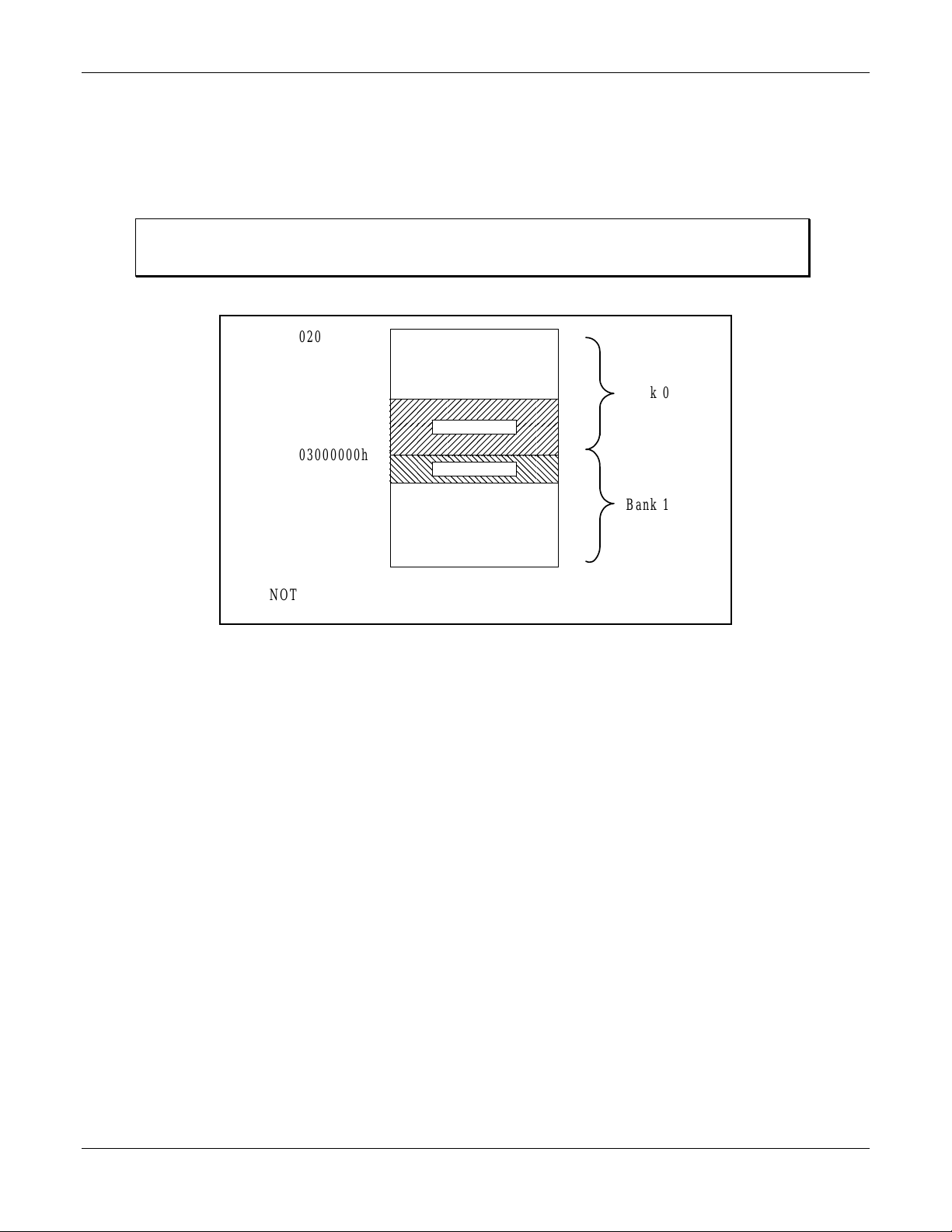
MFC2000 Multifunctional Peripheral Controller 2000 Hardware Description
4.5.1.2 Non-Interleaved DRAM Accesses
Non-interleaved DRAM accesses are available for 8-bit or 16-bit data bus. Byte access is available for both 8-bit
and 16-bit data bus and 16-bit halfword access is available for 16-bit data bus. DRAM early-write mode, normal
read mode and page mode are supported. Read-modify-write is not supported.
Note: 16-bit DRAMs must have upper and lower CAS’s in order to work with the DRAM
controller. 8-bit bursts of data will not work with a 16-bit wide memory structure.
02000000h
02800000h
03000000h
RASn[0]
RASn[1]
Bank 0
03400000h
Bank 1
04000000h
NOTE: In this example, Bank 0 is 8M and Bank 1 is 4M.
Figure 4-15. DRAM Bank/Address Map
4.5.1.3 2-way Interleaved DR AM Acc es ses
The two-way interleaved DRAM interface can support up to four 16-bit wide devices a maximum of 8M deep.
Bank 0 is selected with RASn[0] and bank 1 is selected with RASn[1]. CASEn[1:0], CASOn[1:0], DWRn, DOEOn,
DOEEn, ADDR, and DATA are common between the two banks . 2-way interle a ving is limited to a 16-bit wide
databus. 8-bit or 16-bit wide devices can be used. The ARM CPU can write 32-bit words, 16-bit halfwords or bytes
to the memory banks. The addressing to the interleaved DRAMs starts with address bit 2. Bits 1 and 0 are used
internally to generate the proper CASOn[1:0] and CASEn[1:0] signals. When the memory structure is configured
for two-way interleaving, byte bursts are not allowed. Only bursts of 32-bit words or 16-bit halfwords are allowed.
The maximum burst length is eight 16-bit halfwords. The burst length is controlled by the DRAMBURST signal
that is sent from the SIU. The external memory structure can use the output enables directly to the memory
device or for increased speed can use external bus transceivers. Bus contention must be considered when the
output enables are tied directly to a DRAM memory.
4-56
Conexant
100723A
Page 87

Hardware Description MFC 2000 Multifunctional Peripheral Controller 2000
Table 4-12. Address Multiplexing
Address
Multiplexing
Register
Physical Address ROW COL. ROW COL. ROW COL. ROW COL.
A[13] A[22] A[13] A[23] A[13] A[24] A[13] A[25] A[13]
A[12] A[21] A[12] A[22] A[12] A[23] A[12] A[24] A[12]
A[11] A[20] A[11] A[21] A[11] A[22] A[11] A[23] A[11]
A[10] A[19] A[10] A[20] A[10] A[21] A[10] A[22] A[10]
A[9] A[18] A[9] A[19] A[9] A[20] A[9] A[21] A[9]
A[8] A[17] A[8] A[18] A[8] A[19] A[8] A[20] A[8]
A[7] A[16] A[7] A[17] A[7] A[18] A[7] A[19] A[7]
A[6] A[15] A[6] A[16] A[6] A[17] A[6] A[18] A[6]
A[5] A[14] A[5] A[15] A[5] A[16] A[5] A[17] A[5]
A[4] A[13] A[4] A[14] A[4] A[15] A[4] A[16] A[4]
A[3] A[12] A[3] A[13] A[3] A[14] A[3] A[15] A[3]
A[2] A[11] A[2] A[12] A[2] A[13] A[2] A[14] A[2]
A[1] A[10] A[1] A[11] A[1] A[12] A[1] A[13] A[1]
A[0] A[9] A[0] A[10] A[0] A[11] A[0] A[12] A[0]
Select Option 000 Select Option 001 Select Option 010 Select Option 011
Part 1
Table 4-13. Address Multiplexing
Address
Multiplexing
Register
Physical Address ROW COL. ROW COL. ROW COL. ROW COL.
A[11] A[24] A[13] A[23] A[13] A[24] A[12] A[22] A[12]
A[10] A[23] A[12] A[22] A[12] A[23] A[11] A[21] A[11]
A[9] A[22] A[11] A[21] A[11] A[22] A[10] A[20] A[10]
A[8] A[21] A[10] A[20] A[10] A[21] A[9] A[19] A[9]
A[7] A[20] A[9] A[19] A[9] A[20] A[8] A[18] A[8]
A[6] A[19] A[8] A[18] A[8] A[19] A[7] A[17] A[7]
A[5] A[18] A[7] A[17] A[7] A[18] A[6] A[16] A[6]
A[4] A[17] A[6] A[16] A[6] A[17] A[5] A[15] A[5]
A[3] A[16] A[5] A[15] A[5] A[16] A[4] A[14] A[4]
A[2] A[15] A[4] A[14] A[4] A[15] A[3] A[13] A[3]
A[1] A[14] A[3] A[13] A[3] A[14] A[2] A[12] A[2]
A[0] A[13] A[2] A[12] A[2] A[13] A[1] A[11] A[1]
Select Option 100 Select Option 101 Select Option 110 Select Option 111
Part 2
100723A
Conexant
4-57
Page 88

MFC2000 Multifunctional Peripheral Controller 2000 Hardware Description
Table 4-14. DRAM Row/Column Configuration
Memory Size Address Multiplex
256K x 8 000 000 000 Supported 9 9
256K x 16 DRAMs 000 000 000 Supported 9 9
---
512K x 8 000 000 000 Supported 10 9
1M x 8 001 001 001 Supported 10 10
1M x 16 DRAMs 001 001 001 Supported 10 10
--- --- --- Not S upport ed 12 8
4M x 8 010 010 100 Supported 11 11
4M x 16 DRAMs 001 111 101 Supported 12 10
--- --- --- Not S upport ed 13 9
16M x 8 011 110 --- Supported 12 12
--- --- --- Not S upport ed 13 11
Setting
8-bit 16-bit 2-wy
intrl.
--- --- Not Supported 10 8
Supported/Not Supported Row/Column Configuration
Row Column
4.5.1.4 Refresh Operation
DRAM Refresh is performed automatically using the CAS-before-RAS method. Three different refresh speeds are
supported: slow, normal and fast. These speeds are selected by bits in the backup configuration register. The
refresh time is based on the crystal oscillator frequency and the refresh rate that is selected. During prime power
when it is time to refresh the DRAM, a CAS-before-RAS refresh cycle will be inserted. If the DRAM is being
accessed when a DRAM refresh is requested, the refresh cycle is not inserted until the access is complete. The
maximum burst length that the DRAM Controller will see is 8 halfwords (i.e., the maximum burst length coincides
with the CACHE line size). The maximum burst length is controlled by the SIU with the DRAMBURST signal that
is sent to the DRAM Controller.
4-58
Conexant
100723A
Page 89

Hardware Description MFC 2000 Multifunctional Peripheral Controller 2000
4.5.1.5 Power Down Mode
When the ASIC is powered down, the DRAMs cannot be accessed. Only DRAM refresh will continue on battery
power (VDRAM). Refresh timing is generated from a one shot and an internal gate delay circuit during battery
powered operation. To ensure a smooth transition from VDD refresh to battery powered refresh, a control signal
from the power reset block allows the DRAM controller to switch from VDD refresh to battery refresh when power
is down. When the prime power is reapplied, the refresh logic switches back to VDD refresh. The refresh speed
selected using the BackupConfig register remains in force during the battery backed up mode. The DRAM
Backup time duration is defined by the two DRAM Backup time bits in the BackupConfig register. No backup, 1-2
days, 2-3 days, and infinite are the backup options.
Note: The AMFPC ASIC uses a 3V process; therefore, if the DRAM memory structure is to be
backed up, for the lowest power consumption 3 DRAMs should be used. Also, any external
circuitry must also be battery powered. The output pads of the AMFPC are only 5V tolerant
during high Z. The simplified block diagram for the DRAM controller is illustrated in Figure 4-16.
EXTERNAL ADDRESS
DATABUS
SIU
SIUCLK
DRAMREQ
DRAMRDY
DRAM CNTL.
DRAM ADDR
SIU CNTL
DRAM CONTROL
REGISTER
BATTERY
BACKUP
REGISTER
REFRESH
SPEED
OSCCLK,
CO_1DAY
DRAM CONTROLLER
DRAM STATE
MACHINE
DRAM STATE
MACHINE
BANK 0
BANK 1
BATTERY BACKED UP LOGIC
ONESHOT
SWITCH
DOEOn
DOEEn
RASn[1:0]
CASOn[1:0]
CASEn[1:0]
DWRn
MUX
RTC Battery
DRAM Battery
100723A
Figure 4-16. Simplified DRAM Controller Block Diagram
Conexant
4-59
Page 90

MFC2000 Multifunctional Peripheral Controller 2000 Hardware Description
addr[u:0]
data[7:0]
RASn[1]
DRAM
CASOn[0]
Bank 1
(8-bit
Non-interleaved)
ASIC
DWRn
DOEOn (Wron)
DOEOn (WRon)
data[15:0]
Switch
addr[11:0]
RASn[0]
CASOn[0]
CASOn[1]
DOEen (WRen)
data[15:0]
Switch
addr[11:0]
RASn[0]
CASEn[0]
CASEn[1]
Q-
DWRn
Q-
WEn
OEn
DRAM
OEn
WEn
Bank 0
(Interleaved)
DRAM
OEn
DWRn
WEn
Figure 4-17. DRAM Interface Example
Figure 4-17 gives an example of how each bank of DRAMs might be setup for non-battery back-up DRAM
system. In this example, Bank 0 is setup for an 8-bit non-interleaved memory bank and Bank 1 is setup with a 16bit 2-way interleaved DRAM bank .
Note:
1. DWRn is a battery backed-up signal and is ‘high’ during the battery back-up mode. All inputs
of the prime powered logic will have ‘no power’ or ‘low’ during the battery back-up mode.
Therefore, all external logic, which uses DWRn, should be battery backed-up logic and
should be gated with WRPROTn to ensure that outputs are ‘low’ when the prime power is off
for the battery back-up DRAM operation.
2. DWRn, CASO[1:0]n and CASE[1:0]n are shared by both DRAM banks (RAS[0]n and
RAS[1]n). If you only want to back up one bank by battery power, all shared signals should
be separated by the external logic and should follow the rule in note 2.
4-60
Conexant
100723A
Page 91

Hardware Description MFC 2000 Multifunctional Peripheral Controller 2000
4.5.2 Register Description
Address Bit 15 Bit 14 Bit 13 Bit 12 Bit 11 Bit 10 Bi t 9 Bit 8 Default
DRAM Control
Register
(DRAMCtrl1)
$01FF8821
Address Bi t 7 Bit 6 Bit 5 Bit 4 Bit 3 Bit 2 Bit 1 Bit 0 Default
DRAM Control
Register
(DRAMCtrl1)
$01FF8820
Bank 1 Address Multiplexing Bank 1
Increase
RAS Cycle
Time
Bank 0 Address Multiplexing Bank 0
Increase
RAS Cycle
Time
Bank 1
2-cycle
RAS
Precharge
Bank 0
2-cycle
RAS
Precharge
Bank 1
1-cycle
RAH
Bank 0
1-cycle
RAH
Bank 1 Non-interleaved
Speed Control
00 = Fast Mode
01 = Normal Mode
10 = Slow Mode
11 = N/A
Bank 0 Non-interleaved
Speed Control
00 = Fast Mode
01 = Normal Mode
10 = Slow Mode
11 = N/A
Rst. Value
x0000000b
Read Value
00h
Rst. Value
x0000000b
Read Value
00h
Register Description:
The DRAM Control register is used to program the two DRAM banks for the type of
operation that is desired.
Bits 15-13: Bank 1 Address Multiplexing
Bit 12: Bank 1 Increase RAS Cycle Time
Bit 11: Bank 1 2-cycle RAS Precharge
Bit 10: Bank 1 1-cycle RAH
Bit 9-8: Bank 1 Speed Control
This register controls the addressing multiplexing for Bank 1
This register will add one cycle after the refresh cycle prior to RAS
precharge to meet T
(RASn cycle time). This is needed in order to
RC
use 70 ns DRAMs while running at 39MHz.
This register will increase the RASn[1] Precharge time from 1 to 2
clock cycles.
This register will increase the RASn[1] address hold time. When this
bit is set, the address will be multiplexed 1 clock cycle after the falling
edge of RAS[1]n. The default setting will multiplex the row/column
address ½ clock cycle after the falling edge of RAS[1]n.
These registers will control the speed of the DRAM interface for bank
1 when in the non-interleaved mode. This register controls the width of
the CASn signal. These bits are ignored in interleaved mode.
Bit 9 Bit 8 Non-Interleaved Operation:
0 0 CASn is ½ clock cycle wide.
0 1 CASn is 1 clock cycle wide.
1 0 CASn is 2 clock cycles wide for Read
11 N/A
Bits 7-5: Bank 0 Addressing Multiplexing:
100723A
and 1 clock cycle wide for write.
This register controls the addressing multiplexing for Bank 0
(Table 4-12).
Conexant
4-61
Page 92

MFC2000 Multifunctional Peripheral Controller 2000 Hardware Description
Bit 4: Bank 0 Increase RAS Cycle Time
This register will add one cycle after the refresh cycle prior to RAS
precharge to meet T
(RASn cycle time). This is needed in order to
RC
use 70 ns DRAMs while running at 39MHz.
Bit 3: Bank 0 2-cycle RAS Precharge
This register will increase the RASn[0] Precharge time from 1 to 2
clock cycles.
Bit 2: Bank 0 1-cycle RAH
This register will increase the RASn[0] address hold time. When this
bit is set, the address will be multiplexed 1 clock cycle after the falling
edge of RAS[0]n. The default setting will multiplex the row/column
address ½ clock cycle after the falling edge of RAS[1]n.
Bits 1-0: Bank 0 Speed Control
These registers will control the speed of the DRAM interface for bank
0 when in the non-interleaved mode. This register controls the width of
the CASn signal. These bits are ignored in interleaved mode.
Bit 1 Bit 0 Non-Interleaved Operation
0 0 CASn is ½ clock cycle wide.
0 1 CASn is 1 clock cycle wide.
10
11 N/A
CASn is 2 clock cycles wide for Read
and 1 clock cycle wide for write.
Address Bit 15 Bit 14 Bit 13 Bit 12 Bit 11 Bit 10 Bit 9 Bit 8 Default
Backup
Configuration
Register
(BackupConfig)
$01FF8099
(Not Used) (Not Used) Internal
Power Down
Select
Batrstn
Detected
Lockenn
Timeout
Detected
SRAM
Enable
0 = disable
1 = enable
Bank 1
Data
interface
size:
0 = 8-bit
1 = 16-bit
Bank 0
Data
interface
size:
0 = 8-bit
1 = 16-bit
Rst. Value
xxxxx000b
Read Value
00h
Address Bit 7 Bit 6 Bit 5 Bit 4 Bit 3 Bit 2 Bit 1 Bit 0 Default
Backup
Configuration
Register
(BackupConfig)
$01FF8098
DRAM Backup Time
0 = no backup
1 = 1-2 days
2 = 2-3 days
3 = infinite days
Register Description:
Refresh
Rate
0 = normal
1 = slow
Oscillator
Speed
0 =
32.768 kHz
1 =
65.536 kHz
Bank 1
Enable
0 = disable
1 = enable
Bank 0
Enable
0 = disable
1 = enable
Bank 1
Interleave
Enable
0 = non
interleaved
1 = 2 way
interleaved
Bank 0
Interleave
Enable
0 = non
interleaved
1 = 2 way
interleaved
This register is set to all zeros when first powered up and is battery backed up with the
Rst. Value
00h
Read Value
00h
RTC Battery during power down. When a time out condition occurs, the RASn and CASn signals are tri-stated.
When prime power has returned from a power down sequence, the user will have to perform a checksum on the
DRAM data to know if a time out has occurred since there is no indication that the DRAM battery has lost power.
The user will have to wait 1ms before accessing the DRAM after prime power has returned.
Bits 15-14: Not used
Bit 13: Internal Power Down Select
0 = PWRDWNn is generated by or-ing power_down1 with
power_down2
1= PWRDWNn is generated by and-ing power_down1 with
power_down2
4-62
Conexant
100723A
Page 93

Hardware Description MFC 2000 Multifunctional Peripheral Controller 2000
Note: Power_down1 and power_down2 are output signals from the power-down detection
circuit 1 and 2.
Bit12: Betrstn Detected
This bit indicates that a betrstn occurred. To clear this bit, a 1 must be
written to this bit.
Bit11: This bit indicates that a power down occurred, but no lockout was set
within the 1-2 second period. The lockout timer initiated the lockenn to
create the lockout condition. Once the lockout condition occurs, if the
power down signal is high, the chip will come out of reset after a pud1
delay. To clear this bit a 1 must be written to this bit.
Bit10: SRAM Ch ip Se lec t En abl e
This bit enables the SRAM chip select CSN0.
Bit 9: Bank 1 Interface Size
This register defines whether the data bus to the bank 1 DRAMs is 8
bits wide or 16 bits wide. An 8-bit wide DRAM interf ace uses RASn[ 1]
and CASOn[0]. A 16-bit wide non-interleaved DRAM interface uses
RASn[1] and CASOn[1:0]. A 16-bit wide interleaved DRAM interface
uses RASn[1], CASEn[1:0], and CASOn[1:0].
Bit 8: Bank 0 Interface Size
This register defines whether the data bus to the bank 0 DRAMs is 8
bits wide or 16 bits wide. An 8-bit wide DRAM interf ace uses RASn[ 0]
and CASOn[0]. A 16-bit wide non-interleaved DRAM interface uses
RASn[0] and CASOn[1:0]. A 16-bit wide interleaved DRAM interface
uses RASn[0], CASEn[1:0], and CASOn[1:0].
Bits 7-6: DRAM Battery Backup Time
These bits control the amount of time that the DRAM controller will
spend refreshing the DRAMs when in the battery backup mode. After
reset when the CPU is being released to run, the CPU will not be able
to write data to bits 7 and 6 of the BackupConfig register immediately
since the immediate write will not take effect. The CPU must wait at
least one oscillator clock cycle before writing data into bits 7 and 6.
Bit 7 Bit 6 Battery Backup Duration:
0 0 No battery backup (default)
0 1 1-2 days
1 0 2-3 days
1 1 Infinite
Bit 5-4: DRAM Refresh Rate
These bits are used to set up the DRAM refresh rate. See the following table:
100723A
Conexant
4-63
Page 94

MFC2000 Multifunctional Peripheral Controller 2000 Hardware Description
Refresh
Speed:
(bit 5)
0 0 normal RTC crystal frequency = 32.768 kHz,
0 1 fast RTC crystal frequency = 65.536 kHz,
1 0 slow RTC crystal frequency = 32.768 kHz,
1 1 slow RTC crystal frequency = 65.536 kHz,
Oscillator
Speed:
(bit 4)
Refresh
Speed:
Description:
Refresh clock = the crystal frequency = 32.768 kHz,
The refresh cycle time = 15.625 ms/1024 cycles.
Refresh clock = the crystal frequency = 65.536 kHz,
Refresh cycle time = 7.8125 ms/1024 cycles.
Refresh clock = the crystal frequency/8 = 4.096 kHz
Refresh cycle time = 125 ms/1024 cycles.
Refresh clock = the crystal frequency/16 = 4.096 kHz
Refresh cycle time = 125 ms/1024 cycles.
Bits 3: Bank 1 Enable This bit controls whether or not the Bank 1 DRAMs will be enabled.
The Enable signal will allow CAS before RAS refresh to occur based
on the non-interleave or interleave setting. If the bank setting indicates
a non-interleaved mode, RASn[1] and CASOn[0] (8-bit mode) or
CASOn[1:0] (16-bit mode) will refresh the DRAM. If the bank setting
indicates an interleaved mode, RASn[1], CASOn[1:0] and CASEn[1:0]
will refresh the DRAM. DWRn will be high during refresh. If bank 1 is
disabled, RAS[1]n will be tri-stated and all appropriate CASn’s will be
tri-stated based on mode settings.
Bit 2: Bank 0 Enable This bit controls whether or not the Bank 0 DRAMs will be enabled.
The Enable signal will allow CAS before RAS refresh to occur based
on the non-interleave or interleave setting. If the bank setting indicates
a non-interleaved mode, RASn[0] and CASOn[0] (8-bit mode) or
CASOn[1:0] (16-bit mode) will refresh the DRAM. If the bank setting
indicates an interleaved mode, RASn[0], CASOn[1:0] and CASEn[1:0]
will refresh the DRAM. DWRn will be high during refresh. If bank 0 is
disabled, RAS[0]n will be tri-stated and all appropriate CASn’s will be
tri-stated based on mode settings.
Bit 1: Bank 1 Interleave Enable This register defines whether the bank 1 DRAMs are to be accessed
using 2-way interleave or non interleaved access. 2-way interleaved
access is only valid with a 16-bit interface (the 16 bit vs. 8 bit interface
size bit for bank 1 is ignored by the DRAM controller, but is used by
the SIU to output the data correctly).
Bit 0: Bank 0 Interleave Enable This register defines whether the bank 0 DRAMs are to be accessed
using 2-way interleave or non interleaved access. 2-way interleaved
access is only valid with a 16-bit interface (the 16 bit vs. 8 bit interface
size bit for bank 1 is ignored by the DRAM controller, but is used by
the SIU to output the data correctly).
4-64
Conexant
100723A
Page 95

Hardware Description MFC 2000 Multifunctional Peripheral Controller 2000
4.5.3 Brief Timing
No matter which mode you use and which address you access, the DRAM access timing is lined up with the octal
halfword boundary.
SIUCLK
RASn[0]
CASEn[0]
DOEEn
DWRn
ARM ADDR
or DMA ADDR
SIUADDR
EXTADDR
DATA
a
a
ROW COL
a+2
a+1 a+2
COL COL COL RO W
a+3
a+4
a+4
COL
a+5
COL
OCTAL
BOUNDARY
NOTE: In this example, a =...01010, a+2=...01110, a+4=...10000
Figure 4-18. 8-bit Memory Data Bus
The timing diagram illustrates an 8-bit memory data bus, a burst of halfword transfers (3 halfwords) from the
ARM7 or DMA, for ½ cycle CASn and PG = zero wait states (non-interleaved). It also illustrates the octal halfword
boundary that will cause the SIU to terminate the burst and cause the DRAM Controller to regenerate the RASn
precharge time. This interface speed can only be used at slow frequencies.
SIUCLK
RASn[1]
CASOn[1:0]
DOEOn
DWRn
COL
a+4
a+6
COL
ARMADDR
SIUADDR
DATA
EXTADDR
a
a
ROW COL
a+2 a+4
COL
100723A
Figure 4-19. 16-bit Memory Data Bus
Conexant
4-65
Page 96

MFC2000 Multifunctional Peripheral Controller 2000 Hardware Description
The timing diagram illustrates a 16-bit memory data bus, a burst of word transfers (2 words) from the ARM7 for
full clock width CASn and PG = one wait state (non-interleaved). It also illustrates that the octal halfword boundary
doesn’t occur in the middle of the burst of word transfers.
SIUCLK
RASn[0]
CASEn[0]
DOEEn
DWRn
ARM ADDR
or DMA ADDR
SIU ADDR
DATA
EXT ADDR
ROW COL
a
a
data
Figure 4-20. CASn Non-Interleaved 8-bit DRAM Read
The timing diagram illustrates a two clock cycle CASn non-interleaved 8-bit DRAM read (Non burst mode). This
configuration illustrates the row/column address multiplex occurring 1 cycle after RASn.
SIUCLK
RASn[0]
CASEn[1:0]
CASOn[1:0]
DOEEn
DOEOn
DWRn
ARM ADDR
or DMA ADDR
SIU ADDR
SIU P_ADDR
DATA
EXT ADDR
a +4
a
a
ROW
COL
+2 +6
+2
+2 +6+4
COL
+8
+10
+6+4
+8
COL
+10
+8
+10
4-66
NOTE: In this example, a[2:0] = 00x. Also, the external address is created from the pipelined
SIU address; however, address pins a1 and a0 are not connected to the external memories.
Figure 4-21. 2-Way Interleaved Memory with Halfword Bursts of Data
Conexant
100723A
Page 97

Hardware Description MFC 2000 Multifunctional Peripheral Controller 2000
This example illustrates a read of two-way interleaved memory with halfword bursts of data (6 halfwords). It also
illustrates that the octal halfword boundary doesn’t occur in the middle of the burst of halfword transfers. It
assumes external drivers to minimize the data bus contention and to insure that the data has enough setup time
to CLK. This waveform also illustrates, increased RASn precharge time and increased address multiplexing time.
Byte bursts of data are not allowed when a 16-bit memory structure is used.
SIUCLK
RASn[0]
CASEn[1:0]
CASOn[1:0]
DOEEn
DOEOn
DWRn
ARM ADDR
SIU ADDR
SIU P_ADDR
DATA
EXT ADDR
ROW
a a+4
a
a
COL
+2
+2 +6+4
+6+4
COL
+8
COL
a+8
+10
+8
+10
Figure 4-22. 2-Way Interleaved DRAM Read (3 words)
The timing diagram illustrates a two-way interleaved DRAM read (3 words). It assumes external drivers to
minimize the data bus contention and to insure that the data has enough setup time to CLK. This waveform also
illustrates, increased RASn precharge time and increased address multiplexing time.
SIUCLK
RASn[1]
CASEn[1:0]
CASOn[1:0]
DOEEn
DOEOn
DWRn
ARM ADDR
SIU ADDR
DATA
EXT ADDR
ROW
a a+4 a+8
a
a+2
COL
a+4 a+8
a+6
COL
a+10
COL
100723A
Figure 4-23. 2-Way Interleaved DRAM Write
Conexant
4-67
Page 98

MFC2000 Multifunctional Peripheral Controller 2000 Hardware Description
The timing diagram illustrates two-way interleaved DRAM write. This configuration assumes that the data bus is
available to the DRAM with enough setup time to the CASn falling edge. In addition, this configuration has a 2cycle wide RASn and allows one cycle after the falling edge of RASn before the row/column address mux.
tRPtRAS
SIUCLK
RASn[1]
CASEn[1:0]
CASOn[1:0]
DWRn
tCP
a refresh cycle
Figure 4-24. Refresh Cycle
The timing diagram illustrates a refresh cycle. t
is three cycles wide to accommodate frequency ranges up to
RAS
40 MHz. This timing is used during prime power refresh. During battery backup, a custom refresh circuit is used to
generate refreshed timing based on the oscillator clock.
4.5.4 Detailed Timing Measurements
SIUCLK
t
RD
RASN[1:0]
t
RD
CASEN[1:0],
CASON[1:0]
DWRN
(read)
t
DW
DWRN
(write)
t
RAH1
A[x:0]
(option 1)
A[x:0]
(option 2)
ROW
t
RAH2
ROW COL COL COL
Figure 4-25. DRAM Timing
t
CD
Note:1
Access with 1 or
COL COL COL
t
CDO
t
CD
Note:2
2 wait states
Read, Write and Wait States for Non-interleave Mode
Access with
0 wait states
t
CSU0
t
CSU
t
CD0
t
DW
4-68
Conexant
100723A
Page 99

Hardware Description MFC 2000 Multifunctional Peripheral Controller 2000
SIUCLK
t
RD
RASN[1:0]
t
RD
CASEN[1:0]
Note:1
t
CD
t
CD
t
CD
t
CD
CASON[1:0]
DOEN[1:0]
(WRen/WRon)
t
DW
t
DW
DWRN
SIUCLK
RASN[1:0]
CASEN[1:0]
CASON[1:0]
DOEN[1]
(WRon)
DOEN[0]
(WRen)
Figure 4-26. DRAM Timing for 2-way Interleave Write
t
RD
Note:1
t
t
CD
CD
t
OED
t
OED
t
t
OED
CD
t
CD
t
OED
t
CD
t
OED
t
RD
t
t
OED
CD
100723A
Figure 4-27. DRAM Timing
Conexant
Read for 2-way interleave mode
4-69
Page 100

MFC2000 Multifunctional Peripheral Controller 2000 Hardware Description
SIUCLK
t
RRAS
RASN[1:0]
t
CRD
CASEN[1:0],
CASON[1:0]
t
RCAS
DWRN
Figure 4-28. DRAM Refresh Timing
XIN
RASN[1:0]
CASEN[1:0],
CASON[1:0]
DWRN
t
RRAS
t
RCAS
t
CRD
t
CRD
Figure 4-29. DRAM Battery Refresh Timing
4-70
Conexant
100723A
 Loading...