

Page 1
MF6
6th Order Switched Capacitor Butterworth Lowpass
Filter
General Description
The MF6 is a versatile easy to use, precision 6th order Butterworth lowpass active filter. Switched capacitor techniques
eliminate external component requirements and allow a
clock tunable cutoff frequency. The ratio of the clock frequency to the lowpass cutoff frequency is internally set to 50
to 1 (MF6-50) or 100 to 1 (MF6-100). A Schmitt trigger clock
input stage allows two clocking options, either self-clocking
(via an external resistor and capacitor) for stand-alone applications, or an external TTL or CMOS logic compatible clock
can be used for tighter cutoff frequency control. The maximally flat passband frequency response together with a DC
gain of 1 V/V allows cascading MF6 sections for higher order
filtering. In addition to the filter, two independent CMOS op
amps are included on the die and are useful for any general
signal conditioning applications.
Features
n No external components
n Cutoff frequency accuracy of
±
0.3%typical
n Cutoff frequency range of 0.1 Hz to 20 kHz
n Two uncommitted op amps available
n 5V to 14V total supply voltage
n Cutoff frequency set by external or internal clock
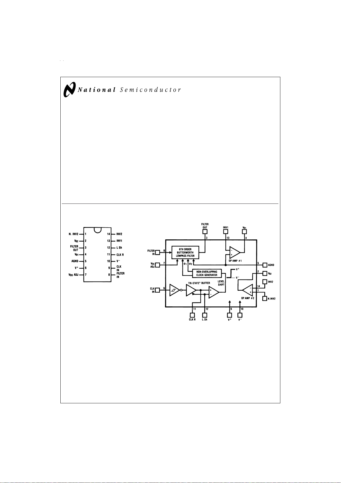
Block and Connection Diagrams
TRI-STATE®is a registered trademark of National Semiconductor Corporation.
All Packages
DS005065-2
Top View
Order Number MF6CWM-50
or MF6CWM-100
See NS Package Number M14B
DS005065-1
June 1999
MF6 6th Order Switched Capacitor Butterworth Lowpass Filter
© 1999 National Semiconductor Corporation DS005065 www.national.com
Page 2
Absolute Maximum Ratings (Note 11)
If Military/Aerospace specified devices are required,
please contact the National Semiconductor Sales Office/
Distributors for availability and specifications.
Supply Voltage 14V
Voltage at Any Pin V
−
− 0.2V, V++ 0.2V
Input Current at Any Pin (Note 13) 5 mA
Package Input Current (Note 13) 20 mA
Power Dissipation (Note 14) 500 mW
Storage Temperature −65˚C to +150˚C
ESD Susceptibility (Note 12) 800V
Soldering Information
Vapor Phase (60 sec.) 215˚C
Infrared (15 sec.) 220˚C
See AN-450 “Surface Mounting Methods and Their Effect
on Product Reliability” (Appendix D) for other methods of
soldering surface mount devices.
Operating Ratings (Note 11)
Temperature Range T
MIN
≤ TA≤ T
MAX
MF6CWM-50, MF6CWM-100 0˚C ≤ TA≤ +70˚C
Supply Voltage (V
S
=
V
+−V−
) 5Vto14V
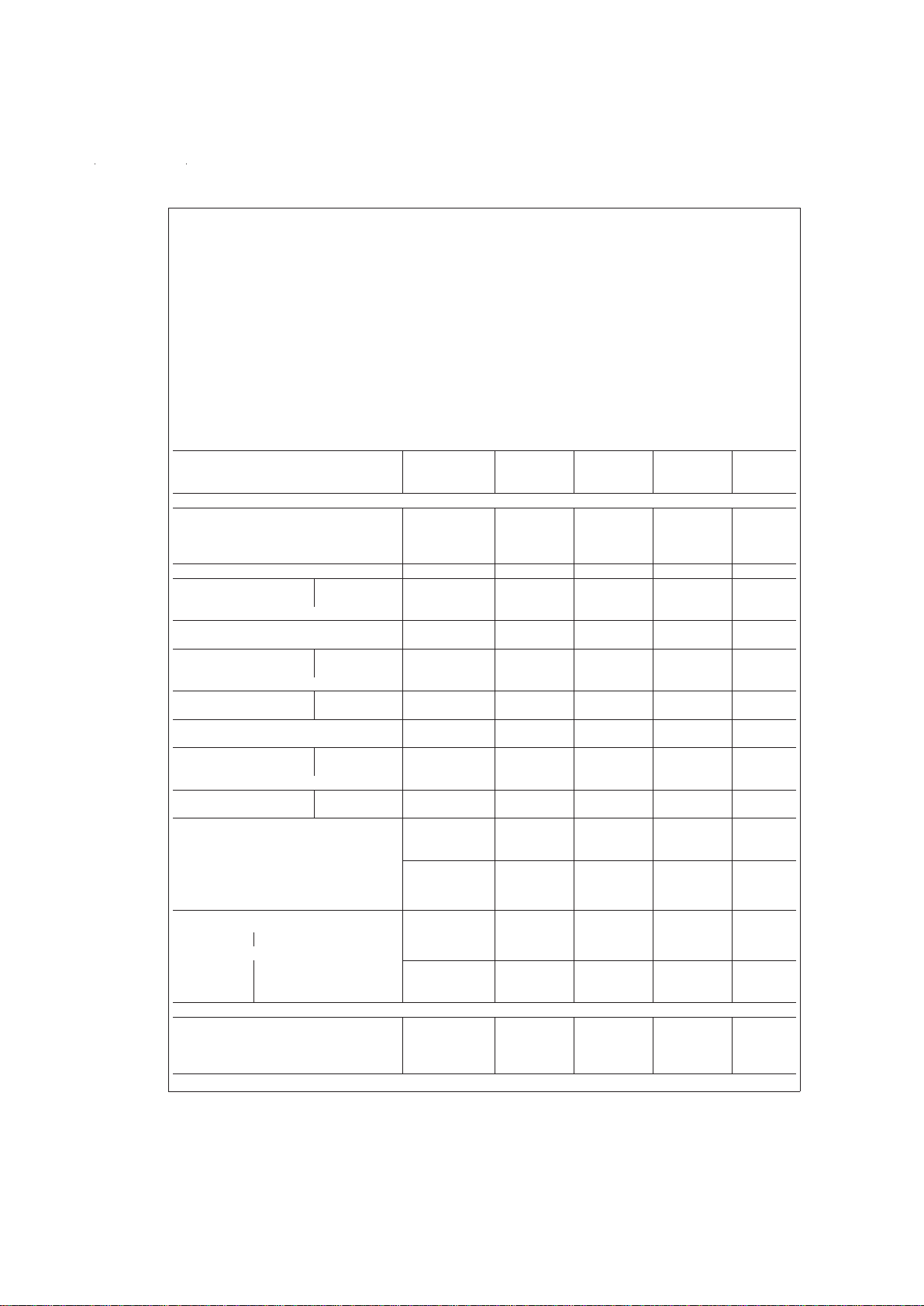
Filter Electrical Characteristics
The following specifications apply for f
CLK
≤ 250 kHz (Note 3) unless otherwise specified. Boldface limits apply for T
MIN
to T
MAX
; all other limits T
A
=
T
J
=
25˚C.
Parameter Conditions Typical Tested Design Units
(Note 8) Limit Limit
(Note 9) (Note 10)
V
+
=
+5V, V
−
=
−5V
f
c
, Cutoff MF6-50 Min 0.1
Frequency Max 20k Hz
Range MF6-100 Min 0.1
(Note 1) Max 10k
Total Supply Current f
CLK
=
250 kHz 4.0 6.0 8.5 mA
Maximum Clock Filter Output 30 mV
Feedthrough Op Amp 1 Out 25 (peak-to-
Op Amp 2 Out 20 peak)
H
o
,R
source
0.0
±
0.30
±
0.30 dB
DC Gain ≤ 2kΩ
f
CLK/fc
MF6-50 49.27±0.3
%
49.27±1
%
49.27±1
%
Clock to Cutoff MF6-100 98.97
±
0.3
%
98.97±1
%
98.97±1
%
Frequency Ratio
DC MF6-50 −200 mV
Offset Voltage MF6-100 −400
Minimum Output R
L
=
10 kΩ +4.0 +3.5 +3.5 V
Voltage Swing −4.1 −3.8 −3.5
Maximum Output Source 50
Short Circuit Sink 1.5 mA
Current (Note 6)
Dynamic Range MF6-50 83 dB
(Note 2) MF6-100 81
Additional MF6-50 f
CLK
=
250 kHz
Magnitude f=6000 Hz −9.47 −9.47
±
0.6 −9.47±0.75 dB
Response Test f=4500 Hz −0.92 −0.92
±
0.6 −0.92±0.4
Points (Note
4)
MF6-100 f
CLK
=
250 kHz
f=3000 Hz −9.48 −9.48
±
0.3 −9.48±0.75 dB
f=2250 Hz −0.97 −0.97
±
0.3 −0.97±0.4
Attenuation
Rate
MF6-50 f
CLK
=
250 kHz
dB/
f
1
=
6000 Hz −36 −36 octave
f
2
=
8000 Hz
MF6-100 f
CLK
=
250 kHz dB/
f
1
=
3000 Hz −36 −36 octave
f
2
=
4000 Hz
V
+
=
+2.5V, V
−
=
−2.5V
f
c
, Cutoff MF6-50 Min 0.1
Frequency Max 10k Hz
Range MF6-100 Min 0.1
(Note 1) Max 5k
www.national.com 2
Page 3
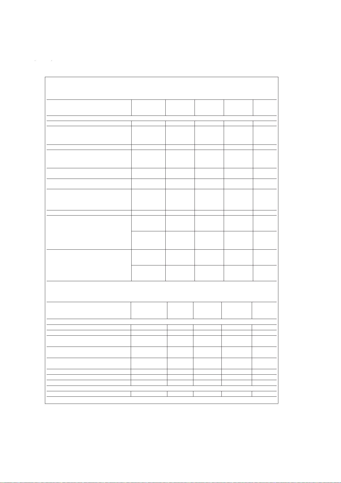
Filter Electrical Characteristics (Continued)
The following specifications apply for f
CLK
≤ 250 kHz (Note 3) unless otherwise specified. Boldface limits apply for T
MIN
to T
MAX
; all other limits T
A
=
T
J
=
25˚C.
Parameter Conditions Typical Tested Design Units
(Note 8) Limit Limit
(Note 9) (Note 10)
V
+
=
+2.5V, V
−
=
−2.5V
Total Supply Current f
CLK
=
250 kHz 2.5 4.0 4.0 mA
Maximum
Clock
Filter Output 20 mV
Feedthrough Op Amp 1 Out 15 (peak-to-
Op Amp 2 Out 10 peak)
H
o
, DC Gain R
source
≤2kΩ 0.0
±
0.30
±
0.30 dB
f
CLK/fc
, Clock to
Cutoff
Frequency
MF6-50 49.10
±
0.3
%
49.10±2
%
49.10±3
%
Ratio MF6-100 98.65
±
0.3
%
98.65±2
%
98.65±2.25
%
DC MF6-50 −200 mV
Offset Voltage MF6-100 −400
Minimum Output R
L
=
10 kΩ +1.5 +1.0 +1.0 V
Voltage Swing −2.2 −1.7 −1.5
Maximum
Output
Source
28
Short Circuit Sink 0.5 mA
Current
(Note 6)
Dynamic Range (Note 2) 77 dB
Additional MF6-50 f
CLK
=
250 kHz
Magnitude f=6000 Hz −9.54 −9.54
±
0.6 −9.54±0.75 dB
Response Test f=4500 Hz −0.96 −0.96
±
0.3 −0.96±0.4
Points (Note
4)
MF6-100 f
CLK
=
250 kHz
f=3000 Hz −9.67 −9.67
±
0.6 −9.67±0.75 dB
f=2250 Hz −1.01 −1.01
±
0.3 −1.01±0.4
Attenuation MF6-50 f
CLK
=
250 kHz dB/
Rate f
1
=
6000 Hz −36 −36 octave
f
2
=
8000 Hz
MF6-100 f
CLK
=
250 kHz dB/
f
1
=
3000 Hz −36 −36 octave
f
2
=
4000 Hz
Op Amp Electrical Characteristics
Boldface limits apply for T
MIN
to T
MAX
; all other limits T
A
=
T
J
=
25˚C.
Parameter Conditions Typical Tested Design Units
(Note 8) Limit Limit
(Note 9) (Note 10)
V
+
=
+5V, V
−
=
−5V
Input Offset Voltage
±
8.0
±
20
±
20 mV
Input Bias Current 10 pA
CMRR (Op Amp
#
2 Only) V
CM1
=
1.8V, 60 55 dB
V
CM2
=
−2.2V
Output Voltage Swing R
L
=
10 kΩ +4.0 +3.8 +3.6 V
−4.5 −4.0 −4.0
Maximum Output Short Source 54 65 80
mA
Circuit Current (Note 6) Sink 2.0 4.0 6.0
Slew Rate 7.0 V/µs
DC Open Loop Gain 72 dB
Gain Bandwidth Product 1.2 MHz
V
+
=
+2.5V, V
−
=
−2.5V
Input Offset Voltage
±
8.0
±
20
±
20 mV
www.national.com3
Page 4
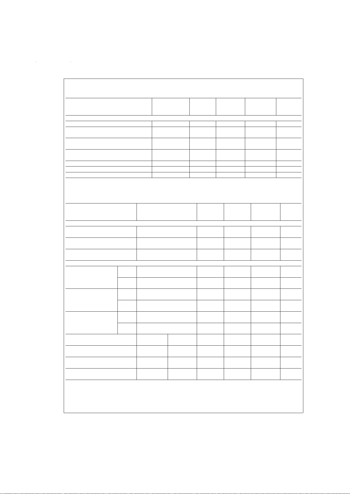
Op Amp Electrical Characteristics (Continued)
Boldface limits apply for T
MIN
to T
MAX
; all other limits T
A
=
T
J
=
25˚C.
Parameter Conditions Typical Tested Design Units
(Note 8) Limit Limit
(Note 9) (Note 10)
V
+
=
+2.5V, V
−
=
−2.5V
Input Bias Current 10 pA
CMRR (Op-Amp
#
2 Only) V
CM1
=
+0.5V, 60 55 dB
V
CM2
=
−0.9V
Output Voltage Swing R
L
=
10 kΩ +1.5 +1.3 +1.1 V
−2.2 −1.7 −1.7
Maximum Output Short Source 24 mA
Circuit Current (Note 6) Sink 1.0
Slew Rate 6.0 V/µs
DC Open Loop Gain 67 dB
Gain Bandwidth Product 1.2 MHz
Logic Input-Output Electrical Characteristics
(Note 5) The following specifications apply for V
−
=
0V unless otherwise specified. Boldface limits apply for T
MIN
to
T
MAX
; all other limits T
A
=
T
J
=
25˚C.
Parameter Conditions Typical Tested Design Units
(Note 8) Limit Limit
(Note 9) (Note 10)
TTL CLOCK INPUT, CLK R PIN (Note 7)
Maximum V
IL
, Logical “0” 0.8 0.8 V
Input Voltage
Minimum V
IH
, Logical “1” 2.0 2.0 V
Input Voltage
Maximum Leakage Current L Sh Pin at 2.0 2.0 µA
at CLK R Pin Mid- Supply
SCHMITT TRIGGER
V
T+
, Positive Going Min V
+
=
10V 7.0 6.1 6.1 V
Threshold Voltage Max 8.9 8.9
Min V
+
=
5V 3.5 3.1 3.1 V
Max 4.4 4.4
V
T−
, Negative Going Min V
+
=
10V 3.0 1.3 1.3 V
Threshold Voltage Max 3.8 3.8
Min V
+
=
5V 1.5 0.6 0.6 V
Max 1.9 1.9
Hysteresis (V
T+−VT−
) Min V
+
=
10V 4.0 2.3 2.3 V
Max 7.6 7.6
Min V
+
=
5V 2.0 1.2 1.2 V
Max 3.8 3.8
Minimum Logical “1” Output
I
o
=
−10µA
V
+
=
10V 9.0 9.0 V
Voltage (Pin 11) V
+
=
5V 4.5 4.5
Maximum Logical “0” Output
I
o
=
10µA
V
+
=
10V 1.0 1.0 V
Voltage (Pin 11) V
+
=
5V 0.5 0.5
Minimum Output Source CLK R Tied V
+
=
10V 6.0 3.0 3.0 mA
Current (Pin 11) to Ground V
+
=
5V 1.5 0.75 0.75
Maximum Output Sink CLK R Tied V
+
=
10V 5.0 2.5 2.5 mA
Current (Pin 11) to V
+
V
+
=
5V 1.3 0.65 0.65
Note 1: The cutoff frequency of the filter is defined as the frequency where the magnitude response is 3.01 dB less than the DC gain of the filter.
Note 2: For
±
5V supplies the dynamic range is referenced to 2.82 Vrms (4V peak) where the wideband noise over a 20 kHz bandwidth is typically 200 µVrms for
the MF6-50 and 250 µVrmsfortheMF6-100.For
±
2.5V supplies the dynamic range isreferencedto1.06Vrms (1.5V peak) where the widebandnoiseovera20kHz
bandwidth is typically 140 µVrms for both the MF6-50 and the MF6-100.
Note 3: The specifications for the MF6 have been given for a clock frequency (f
CLK
) of 250 kHz and less. Above this clock frequency the cutoff frequency begins to
deviate from the specified error band of
±
1.0%but the filter still maintains its magnitude characteristics. See Application Hints, Section 1.5.
www.national.com 4
Page 5
Logic Input-Output Electrical Characteristics (Continued)
Note 4: Besides checking the cutoff frequency (fc) and the stopband attenuation at 2 fc, two additional frequencies are used to check the magnitude response of the
filter. The magnitudes are referenced to a DC gain of 0.0 dB.
Note 5: For simplicity all the logic levels have been referenced to V
−
=
0V and will scale accordingly for
±
5V and±2.5V supplies (except for the TTL input logic lev-
els).
Note 6: The short circuit source current is measured by forcing the output that is being tested to its maximum positive voltage swing and then shorting that output
to the negative supply. The short circuit sink current is measured by forcing the output that is being tested to its maximum negative voltage swing and then shorting
that output to the positive supply. These are the worst-case conditions.
Note 7: The MF6 is operating with symmetrical split supplies and L.Sh is tied to ground.
Note 8: Typicals are at 25˚C and represent most likely parametric norm.
Note 9: Tested limits are guaranteed to National’s AOQL (Average Outgoing Quality Level).
Note 10: Design limits are guaranteed, but not 100%tested. These limits are not used to calculate outgoing quality levels.
Note 11: Absolute Maximum Ratings indicate limits beyond which damage to the device mayoccur. DC andACelectricalspecifications do not apply when operating
the device beyond its specified conditions.
Note 12: Human body model, 100 pF discharged through a 1.5k Ω resistor.
Note 13: When the input voltage (V
IN
) at any pin exceeds the power supply rails (V
IN
<
V−or V
IN
>
V+) the absolute value of current at that pin should be limited
to 5 mA or less. The 20 mA package input current limits the number of pins that can exceed the power supply boundaries witha5mAcurrent limit to four.
Note 14: The maximum power dissipation must be derated at elevated temperatures and is dictated by T
JMAX
, θJA, and the ambient temperature, TA. The maximum
allowable power dissipation at any temperature is P
D
=
(T
JMAX−TA
)/θJAor the number given in the Absolute Maximum Ratings, whichever is lower. For this device,
T
JMAX
=
125˚C, and the typical junction-to-ambient thermal resistance is 78˚C/W. For the MF6CJ this number decreases to 62˚C/W. For MF6CWM, θ
JA
=
78˚C/W.
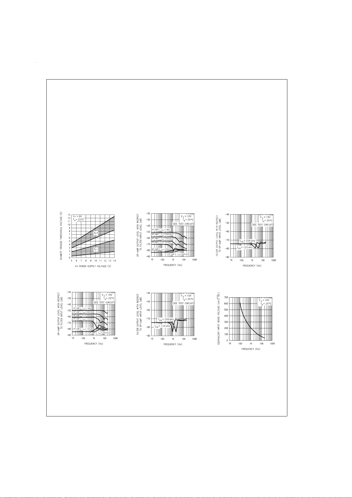
Typical Performance Characteristics
Schmitt Trigger Threshold Voltage
vs Power Supply Voltage
DS005065-40
Crosstalk from Filter
to Op-Amps (MF6-100)
DS005065-41
Crosstalk from Either Op-Amp
to Filter Output (MF6-50)
DS005065-42
Crosstalk from Filter
to Op-Amps (MF6-50)
DS005065-43
Crosstalk from Either Op-Amp to
Filter Output (MF6-100)
DS005065-44
Equivalent Input Noise
Voltage of Op-Amps
DS005065-45
www.national.com5
Page 6
Typical Performance Characteristics (Continued)
Positive Voltage Swing vs
Power Supply Voltage
(Op Amp Output)
DS005065-46
Positive Voltage Swing vs
Power Supply Voltage
(Filter Output)
DS005065-47
Positive Voltage Swing vs
Temperature (Filter and
Op Amp Outputs)
DS005065-48
Negative Voltage Swing vs
Power Supply Voltage
(Filter and Op Amp Outputs)
DS005065-49
Negative Voltage Swing vs
Temperature (Filter and
Op Amp Outputs)
DS005065-50
Power Supply Current vs
Clock Frequency
DS005065-51
Power Supply Current
vs Temperature
DS005065-52
Power Supply Current
vs Power Supply Voltage
DS005065-53
f
CLK/fc
Deviation
vs Clock Frequency
DS005065-54
www.national.com 6
Page 7

Typical Performance Characteristics (Continued)
f
CLK/fc
Deviation
vs Temperature
DS005065-55
f
CLK/fc
Deviation
vs Power Supply Voltage
DS005065-56
f
CLK/fc
Deviation
vs Clock Frequency
DS005065-57
f
CLK/fc
Deviation
vs Temperature
DS005065-58
f
CLK/fc
Deviation
vs Power Supply Voltage
DS005065-59
DC Gain Deviation
vs Temperature
DS005065-60
DC Gain Deviation
vs Power Supply Voltage
DS005065-61
DC Gain Deviation
vs Clock Frequency
DS005065-62
DC Gain Deviation
vs Temperature
DS005065-63
www.national.com7
Page 8

Typical Performance Characteristics (Continued)
Crosstalk Test Circuits
Pin Descriptions
(Pin Numbers)
Pin Description
FILTER OUT
(3)
The output of the lowpass filter. It
will typically sink 0.9 mA and source
3 mA and swing to within 1V of each
supply rail.
FILTER IN (8) The input to the lowpass filter. To
minimize gain errors the source
impedance that drives this input
should be less than 2k (see section
1.4). For single supply operation the
input signal must be biased to
mid-supply or AC coupled.
Pin Description
V
OS
ADJ (7) This pin is used to adjust the DC
offset of the filter output; if not used
it must be tied to the AGND
potential. (See section 1.3)
DC Gain Deviation
vs Power Supply Voltage
DS005065-64
DC Gain Deviation
vs Clock Frequency
DS005065-65
From Filter to Op Amps
DS005065-10
From Either Op Amp to Filter Output
DS005065-11
www.national.com 8
Page 9

Pin Descriptions (Pin Numbers) (Continued)
Pin Description
AGND (5) The analog ground pin. This pin sets
the DC bias level for the filter section
and the non-inverting input of
Op-Amp
#
1 and must be tied to the
system ground for split supply
operation or to mid-supply for single
supply operation (see section 1.2).
When tied to mid-supply this pin
should be well bypassed.
V
O1
(4),
INV1 (13)
VO1is the output and INV1 is the
inverting input of Op-Amp
#
1. The
non-inverting input of this Op-Amp is
internally connected to the AGND
pin.
V
O2
(2),
INV2 (14),
NINV2 (1)
V
O2
is the output, INV2 is the
inverting input, and NINV2 is the
non-inverting input of Op-Amp
#
2.
V
+
(6), V−(10) The positive and negative supply
pins. The total power supply range is
5V to 14V. Decoupling these pins
with 0.1 µF capacitors is highly
recommended.
CLK IN (9) A CMOS Schmitt-trigger input to be
used with an external CMOS logic
level clock. Also used for
self-clocking Schmitt-trigger oscillator
(see section 1.1).
CLK R (11) A TTL logic level clock input when in
split supply operation (
±
2.5V to
±
7V) and L. Sh tied to system
ground. This pin becomes a low
impedance output when L. Sh is tied
to V
−
. Also used in conjunction with
the CLK IN pin for a self clocking
Schmitt-trigger oscillator (see section
1.1).
L. Sh (12) Level shift pin, selects the logic
threshold levels for the desired
clock. When tied to V
−
it enables an
internal tri-state
®
buffer stage
between the Schmitt trigger and the
internal clock level shift stage thus
enabling the CLK IN Schmitt-trigger
input and making the CLK R pin a
low impedance output.
When the voltage level at this input
exceeds [25%(V
+−V−
)+V−] the
internal tri-state buffer is disabled
allowing the CLK R pin to become
the clock input for the internal clock
level shift stage. The CLK R
threshold level is now 2V above the
voltage applied to the L. Sh pin.
Driving the CLK R pin with TTL logic
levels can be accomplished through
the use of split supplies and by tying
the L. Sh pin to system ground.
www.national.com9
Page 10

1.0 MF6 Application Hints
The MF6 is comprised of a non-inverting unity gain lowpass
sixth order Butterworth switched capacitor filter section and
two undedicated CMOS Op-Amps. The switched capacitor
topology makes the cutoff frequency (where the gain drops
3.01 dB below the DC gain) a direct ratio (100:1 or 50:1) of
the clock frequency supplied to the lowpass filter. Internal integrator time constants set the filter’s cutoff frequency. The
resistive element of these integrators is actually a capacitor
which is “switched” at the clock frequency (for a detailed discussion see Input Impedance Section). Varying the clock frequency changes the value of this resistive element and thus
the time constant of the integrators. The clock to cutoff frequency ratio (f
CLK/fc
) is set by the ratio of the input and feed-
back capacitors in the integrators. The higher the clock to
cutoff frequency ratio (or the sampling rate) the closer this
approximation is to the theoretical Butterworth response.
The MF6 is available in f
CLK/fc
ratios of 50:1 (MF6-50) or
100:1 (MF6-100).
1.1 CLOCK INPUTS
The MF6 has a Schmitt-trigger inverting buffer which can be
used to construct a simple R/C oscillator. The oscillator’s frequency is dependent on the buffer’s threshold levels as well
as on the resistor/capacitor tolerance (see
Figure 1
).
DS005065-12
FIGURE 1. Schmitt Trigger R/C Oscillator
www.national.com 10
Page 11

1.0 MF6 Application Hints (Continued)
DS005065-3
FIGURE 2. Dual Supply Operation
MF6 Driven with CMOS Logic Level Clock
(V
IH
≥ 0.8 VCCand VIL≤ 0.2 VCCwhere V
CC
=
V
+−V−
)
DS005065-4
FIGURE 3. Dual Supply Operation
MF6 Driven with TTL Logic Level Clock
www.national.com11
Page 12

1.0 MF6 Application Hints (Continued)
DS005065-14
a) Resistor Biasing of AGND
DS005065-15
b) Using Op-Amp 2 to Buffer AGND
FIGURE 4. Single Supply Operation
www.national.com 12
Page 13

1.0 MF6 Application Hints (Continued)
Schmitt-trigger threshold voltage levels can change significantly causing the R/C oscillator’s frequency to vary greatly
from part to part.
Where accuracy in f
c
is required an external clock can be
used to drive the CLK R input of the MF6. This input is TTL
logic level compatible and also presents a very light load to
the external clock source (
z
2 µA) with split supplies and
L. Sh tied to system ground. The logic level is programmed
by the voltage applied to level shift (L. Sh) pin (See the Pin
description for L. Sh pin).
1.2 POWER SUPPLY BIASING
The MF6 can be biased from a single supply or dual split
supplies. The split supply mode shown in
Figure 2
and
Fig-
ure 3
is the most flexible and easiest to implement. As dis-
cussed earlier split supplies,
±
5V to±7V,will enable the use
of TTL or CMOS clock logic levels.
Figure 4
shows two
schemes for single supply biasing. In this mode only CMOS
clock logic levels can be used.
1.3 OFFSET ADJUST
The VosADJ pin is used in adjusting the output offset level of
the filter section. If this pin is not used it must be tied to the
analog ground (AGND) level, either mid-supply for single
ended supply operation or ground for split supply operation.
This pin sets the zero reference for the output of the filter.
The implementation of this pin can be seen in
Figure 5
.In
Figure 5a
, DC offset is adjusted using a potentiometer; in
Figure 5b
, the Op-Amp integrator circuit keeps the average
DC output level at AGND. The circuit in
Figure 5b
is therefore
appropriate only for AC-coupled signals and signals biased
at AGND.
1.4 INPUT IMPEDANCE
The MF6 lowpass filter input (FILTERIN pin) is not a high impedance buffer input. This input is a switched capacitor resistor equivalent, and its effective impedance is inversely
proportional to the clock frequency. The equivalent circuit of
the input to the filter can be seen in
Figure 6
. The input ca-
pacitor charges to the input voltage (V
in
) during one half of
the clock period, during the second half the charge is transferred to the feedback capacitor. The total transfer of charge
in one clock cycle is therefore Q=C
inVin
, and since current
is defined as the flow of charge per unit time the average input current becomes
I
in
=
Q/T
DS005065-16
DS005065-17
FIGURE 5. VOSAdjust Schemes
DS005065-18
a) Equivalent Circuit for MF6 Filter Input
DS005065-19
b) Actual Circuit for MF6 Filter Input
FIGURE 6. MF6 Filter Input
www.national.com13
Page 14
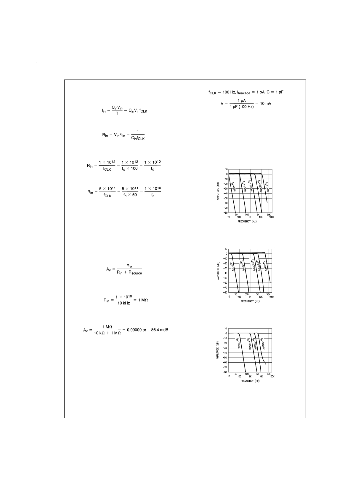
1.0 MF6 Application Hints (Continued)
(where T equals one clock period) or
The equivalent input resistor (Rin) then can be defined as
The input capacitor is 2 pF for the MF6-50 and 1 pF for the
MF6-100, so for the MF6-100
and
for the MF6-50. As shown in the above equations for a given
cutoff frequency (f
c
) the input impedance remains the same
for the MF6-50 and the MF6-100. The higher the clock to
center frequency ratio, the greater equivalent input resistance for a given clock frequency. As the cutoff frequency increases the equivalent input impedance decreases. This input resistance will form a voltage divider with the source
impedance (R
source
). Since Rinis inversely proportional to
the cutoff frequency, operation at higher cutoff frequencies
will be more likely to load the input signal which would appear as an overall decrease in gain to the output of the filter.
Since the filter’s ideal gain is unity its overall gain is given by:
If the MF6-50 or the MF6-100 were set up for a cutoff frequency of 10 kHz the input impedance would be:
In this example with a source impedance of 10k the overall
gain, if the MF6 had an ideal gain of 1 or 0 dB, would be:
Since the maximum overall gain error for the MF6 is±0.3 dB
with a R
s
≤ 2kΩthe actual gain error for this case would be
+0.21 dB to −0.39 dB.
1.5 CUTOFF FREQUENCY RANGE
The filter’s cutoff frequency (f
c
) has a lower limit caused by
leakage currents through the internal switches discharging
the stored charge on the capacitors. At lower clock frequencies these leakage currents can cause millivolts of error, for
example:
The propagation delay in the logic and the settling time required to acquire a new voltage level on the capacitors increases as the MF6 power supply voltage decreases. This
causes a shift in the f
CLK/fc
ratio which will become noticeable when the clock frequency exceeds 250 kHz. The amplitude characteristic will stay within tolerance until f
CLK
exceeds 500 kHz and will peak at about 0.5 dB at the corner
frequency with a 1 MHz clock. The response of the MF6 is
still a reasonable approximation of the ideal Butterworth lowpass characteristic as can be seen in
Figures 7, 8, 9, 10
.
DS005065-20
FIGURE 7. MF6-100±5V Supplies
Amplitude Response
DS005065-21
FIGURE 8. MF6-50±5V Supplies
Amplitude Response
DS005065-22
FIGURE 9. MF6-100±2.5V Supplies
Amplitude Response
www.national.com 14
Page 15

1.0 MF6 Application Hints (Continued)
2.0 Designing with the MF6
Given any lowpass filter specification two equations will
come in handy in trying to determine whether the MF6 will do
the job. The first equation determines the order of the lowpass filter required:
where n is the order of the filter, A
min
is the minimum stop-
band attenuation (in dB) desired at frequency f
s
, and A
max
is
the passband ripple or attenuation (in dB) at frequency f
b
.If
the result of this equation is greater than 6, then more than a
single MF6 is required.
The attenuation at any frequency can be found by the following equation:
Attn(f)=10 log [1 + (10
0.1A max
−1) (f/fb)2n] dB (2)
where n=6 (the order of the filter).
2.1 A LOWPASS DESIGN EXAMPLE
Suppose the amplitude response specification in
Figure 11
is
given. Can the MF6 be used? The order of the Butterworth
approximation will have to be determined using eq. 1:
A
min
=
30 dB, A
max
=
1.0 dB, f
s
=
2 kHz, and f
b
=
1 kHz
Since n can only take on integer values, n=6. Therefore the
MF6 can be used. In general, if n is 6 or less a single MF6
stage can be utilized.
Likewise, the attenuation at f
s
can be found using equation 2
with the above values and n=6 giving:
Atten (2 kHz)=10log[1+(10
0.1
− 1) (2 kHz/1 kHz)12]
=
30.26 dB
This result also meets the design specification given in
Figure 11
again verifying that a single MF6 section will be
adequate.
Since the MF6’s cutoff frequency f
c
, which corresponds to a
gain attenuation of −3.01 dB, was not specified in this example it needs to be calculated. Solving equation 2 where
f=f
c
as follows:
To implement this example for the MF6-50 the clock frequency will have to be set to f
CLK
=
50(1.116 kHz)=55.8
kHz or for the MF6-100 f
CLK
=
100(1.116 kHz)=111.6 kHz.
2.2 CASCADING MF6s
In the case where a steeper stopband attenuation rate is required two MF6’s can be cascaded (
Figure 12
) yielding a
12th order slope of 72 dB per octave. Because the MF6 is a
Butterworth filter and therefore has no ripple in its passband,
when MF6s are cascaded the resulting filter also has no
ripple in its passband. Likewise the DC and passband gains
will remain at 1V/V. The resulting response is shown in
Figures 13, 14
.
In determining whether the cascaded MF6s will yield a filter
that will meet a particular amplitude response specification,
as above, equations 3 and 4 can be used, shown below.
where n=6 (the order of each filter).
Equation 3 will determine whether the order of the filter is ad-
equate (n ≤ 6) while equation 4 can determine if the required
stopband attenuation is met and what actual cutoff frequency
(f
c
) is required to obtain the particular frequency response
desired. The design procedure would be identical to the one
shown in section 2.1.
DS005065-23
FIGURE 10. MF6-50±2.5V Supplies
Amplitude Response
DS005065-24
FIGURE 11. Design Example Magnitude Response
Specification Where the Response of the Filter Design
Must Fall Within the Shaded Area of the Specification
www.national.com15
Page 16

2.0 Designing with the MF6 (Continued)
2.3 IMPLEMENTING A “NOTCH” FILTER WITH THE MF6
A “notch” filter with 60 dB of attenuation can be obtained by
using one of the Op-Amps, available in the MF6, and three
external resistors. The circuit and amplitude response are
shown in
Figures 15, 16
.
The frequency where the “notch” will occur is equal to the
frequency at which the output signal of the MF6 will have the
same magnitude but be 180 degrees out of phase with its input signal. For a sixth order Butterworth filter 180˚ phase
shift occurs where f=f
n
=
0.742 f
c
. The attenuation at this
frequency is 0.12 dB which must be compensated for by
making R
1
=
1.014 x R
2
.
Since R
1
does not equal R2there will be a gain inequality
above and below the notch frequency. At frequencies below
the notch frequency (f
<<
fn), the signal through the filter
has a gain of one and is non-inverting. Summing this with the
input signal through the Op-Amp yields an overall gain of two
or +6 dB. For f
>>
fn, the signal at the output of the filter is
greatly attenuated thus only the input signal will appear at
the output of the Op-Amp. With R
3
=
R
1
=
1.014 R
2
the over-
all gain is 0.986 or −0.12 dB at frequencies above the notch.
DS005065-25
FIGURE 12. Cascading Two MF6s
DS005065-26
FIGURE 13. One MF6-50 vs. Two MF6-50s Cascaded
DS005065-27
FIGURE 14. Phase Response of
Two Cascaded MF6-50s
www.national.com 16
Page 17

2.0 Designing with the MF6 (Continued)
2.4 CHANGING CLOCK FREQUENCY
INSTANTANEOUSLY
The MF6 will respond favorably to a sudden change in clock
frequency. Distortion in the output signal occurs at the transition of the clock frequency and lasts approximately three
cutoff frequency (f
c
) cycles. As shown in
Figure 17
,ifthe
control signal is low the MF6-50 has a 100 kHz clock making
f
c
=
2 kHz; when this signal goes high the clock frequency
changes to 50 kHz yielding 1 kHz f
c
.
The transient response of the MF6 seen in
Figure 18
is also
dependent on the f
c
and thus the f
CLK
applied to the filter.
The MF6 responds as a classical sixth order Butterworth
lowpass filter.
DS005065-28
FIGURE 15. “Notch” Filter
DS005065-29
FIGURE 16. MF6-50 “Notch” Filter Amplitude Response
www.national.com17
Page 18

2.0 Designing with the MF6 (Continued)
2.5 ALIASING CONSIDERATIONS
Aliasing effects have to be taken into consideration when input signal frequencies exceed half the sampling rate. For the
MF6 this equals half the clock frequency (f
CLK
). When the input signal contains a component at a frequency higher than
half the clock frequency, as in
Figure 19a
, that component
will be “reflected” about f
CLK
/2 into the frequency range
be-
low
f
CLK
/2 as in
Figure 19b
. If this component is within the
passband of the filter and of large enough amplitude it can
cause problems. Therefore if frequency components in the
input signal exceed f
CLK
/2 they must be attenuated before
being applied to the MF6 input. The necessary amount of attenuation will vary depending on system requirements. In
critical applications the signal components above f
CLK
/2 will
have to be attenuated at least to the filter’s residual noise
level. An example circuit is shown in
Figure 20
using one of
the uncommitted Op-Amps available in the MF6.
DS005065-30
f
IN
=
1.5 kHz (scope time base=2 ms/div)
FIGURE 17. MF6-50 Abrupt Clock Frequency Change
DS005065-31
FIGURE 18. MF6-50 Step Input Response, Vertical
=
2V/div., Horizontal=1 ms/div., f
CLK
=
100 kHz
DS005065-37
(a) Input Signal Spectrum
DS005065-38
(b) Output Signal Spectrum. Note that the input signal
at f
s
/2 + f causes an output signal to appear at fs/2−f.
FIGURE 19. The phenomenon of aliasing in sampled-data systems. An input signal whose frequecy is greater than
one-half the sampling frequency will cause an output to appear at a frequency lower than one-half the sampling
frequency. In the MF6, f
sfCLK
.
www.national.com 18
Page 19

2.0 Designing with the MF6 (Continued)
DS005065-34
Note: The parallel combination of R4(if used), R1and R2should be ≥ 10 kΩ in order not to load Op-Amp#2.
FIGURE 20. Second Order Butterworth Anti-Aliasing Filter Using Uncommitted Op-Amp#2
www.national.com19
Page 20

Physical Dimensions inches (millimeters) unless otherwise noted
LIFE SUPPORT POLICY
NATIONAL’S PRODUCTS ARE NOT AUTHORIZED FOR USE AS CRITICAL COMPONENTS IN LIFE SUPPORT
DEVICES OR SYSTEMS WITHOUT THE EXPRESS WRITTEN APPROVAL OF THE PRESIDENT AND GENERAL
COUNSEL OF NATIONAL SEMICONDUCTOR CORPORATION. As used herein:
1. Life support devices or systems are devices or
systems which, (a) are intended for surgical implant
into the body, or (b) support or sustain life, and
whose failure to perform when properly used in
accordance with instructions for use provided in the
labeling, can be reasonably expected to result in a
significant injury to the user.
2. A critical component is any component of a life
support device or system whose failure to perform
can be reasonably expected to cause the failure of
the life support device or system, or to affect its
safety or effectiveness.
National Semiconductor
Corporation
Americas
Tel: 1-800-272-9959
Fax: 1-800-737-7018
Email: support@nsc.com
National Semiconductor
Europe
Fax: +49 (0) 1 80-530 85 86
Email: europe.support@nsc.com
Deutsch Tel: +49 (0) 1 80-530 85 85
English Tel: +49 (0) 1 80-532 78 32
Français Tel: +49 (0) 1 80-532 93 58
Italiano Tel: +49 (0) 1 80-534 16 80
National Semiconductor
Asia Pacific Customer
Response Group
Tel: 65-2544466
Fax: 65-2504466
Email: sea.support@nsc.com
National Semiconductor
Japan Ltd.
Tel: 81-3-5639-7560
Fax: 81-3-5639-7507
www.national.com
Small Outline Wide Body (M)
Order Number MF6CWM-50 or MF6CWM-100
NS Package Number M14B
MF6 6th Order Switched Capacitor Butterworth Lowpass Filter
National does not assume any responsibility for use of any circuitry described, no circuit patent licenses are implied and National reserves the right at any time without notice to change said circuitry and specifications.
 Loading...