

A
Dual N-Channel 30-V(D-S) MOSFET
ME4932A/ME4932A-G
GENERAL DESCRIPTION
The ME4932A is the Dual N-Channel logic enhancement mode
power field effect transistors are produced using high cell density ,
DMOS trench technology integrated Schottky diode. This high
density process is especially tailored to minimize on-state resistance.
These devices are particularly suited for low voltage application such
as cellular phone and notebook computer power management and
other battery powered circuits where high-side switching , and low
in-line power loss are needed in a very small outline surface mount
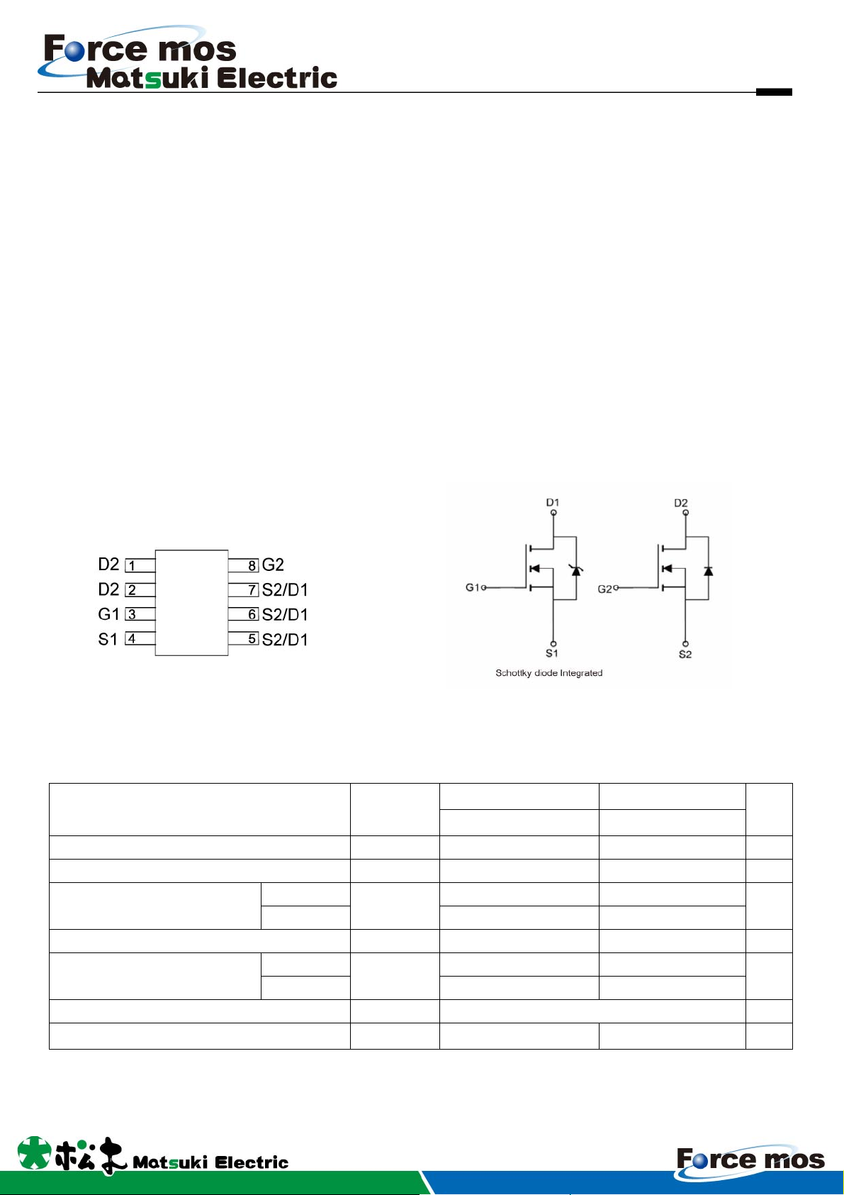
PIN CONFIGURATION
(SOP-8)
Top View
FEATURES
● Schottky diode Integrated
● FET1:RDS(ON)≦12mΩ@VGS=10V
● FET1:RDS(ON)≦22mΩ@VGS=4.5V
● FET2:RDS(ON)≦15.8mΩ@VGS=10V
● FET2:RDS(ON)≦23mΩ@VGS=4.5V
● Super high density cell design for extremely low RDS(ON)
● Exceptional on-resistance and maximum DC current
capability
APPLICATIONS
● Power Management in Note book
● Battery Powered System
Ordering Information: ME4932A (Pb-free)
ME4932A-G (Green product- Halogen free)
Absolute Maximum Ratings (TA=25℃ Unless Otherwise Noted)
Drain-Source Voltage VDSS 30 30 V
Gate-Source Voltage VGSS ±20 ±20 V
Continuous Drain
Pulsed Drain Current IDM 41 36 A
Maximum Power Dissipation*
Operating Junction Temperature TJ -55 to 150 ℃
Thermal Resistance-Junction to Ambient*
Parameter Symbol
TA=25℃ 10.2 9
TA=70℃
TA=25℃ 2 2
TA=70℃
FET1 FET2
Maximum Ratings Maximum Ratings
ID
PD
θJA 62.5 62.5
R
8.2 7.2
1.3 1.3
Unit
A
W
℃/W
* The device mounted on 1in
ug, 2011-Ver1.0
Jul, 2012-Ver1.3
2
FR4 board with 2 oz copper
01
A
FET1
ME4932A/ME4932A-G
Dual N-Channel 30-V(D-S) MOSFET
Electrical Characteristics (TA =25℃ Unless Otherwise Specified)
Symbol Parameter Limit Min Typ Max Unit
STATIC
GS=0V, ID=250μA
BVDSS Drain-Source Breakdown Voltage
VGS(th) Gate Threshold Voltage
IGSS Gate Leakage Current VDS=0V, VGS=±20V ±100 nA
IDSS Zero Gate Voltage Drain Current VDS=30V, VGS=0V 0.1 mA
V
DS=VGS, ID=250μA
V
30 V
1 3 V
RDS(ON)
Drain-Source On-State Resistance
a
VSD Diode Forward Voltage IS=1A, VGS=0V 0.47 0.56 V
DYNAMIC
Qg Total Gate Charge VDS=15V, VGS=10V, ID=11.2A
Qg Total Gate Charge
Qgs Gate-Source Charge
Qgd Gate-Drain Charge
Ciss Input capacitance 865
Coss Output Capacitance 295
Crss Reverse Transfer Capacitance
Rg Gate-Resistance VDS=0V, V
td(on)
tr
td(off)
tf
Turn-On Delay Time
Turn-On Rise Time
Turn-Off Delay Time
Turn-Off Fall Time
VGS=10V, ID= 11.2A 9.5 12
V
GS=4.5V, ID= 8A 16 22
21
11
5
4.6
15
14
41
4
V
DS=15V, VGS=4.5V, D=11.2A
V
DS=15V, VGS=0V, f=1.0MHz
=0V, f=1MHz 0.6
GS
V
DD=15V, RL =15Ω
I
D=1A, VGEN=10V
R
G=3Ω
153
mΩ
nC
pF
Ω
ns
Notes: a. Pulse test: pulse width≦ 300us, duty cycle≦ 2%, Guaranteed by design, not subject to production testing.
b. Matsuki Electric/ Force mos reserves the right to improve product design, functions and reliability without notice.
ug, 2011-Ver1.0
Jul, 2012-Ver1.3
02
A
Dual N-Channel 30-V(D-S) MOSFET
ME4932A/ME4932A-G
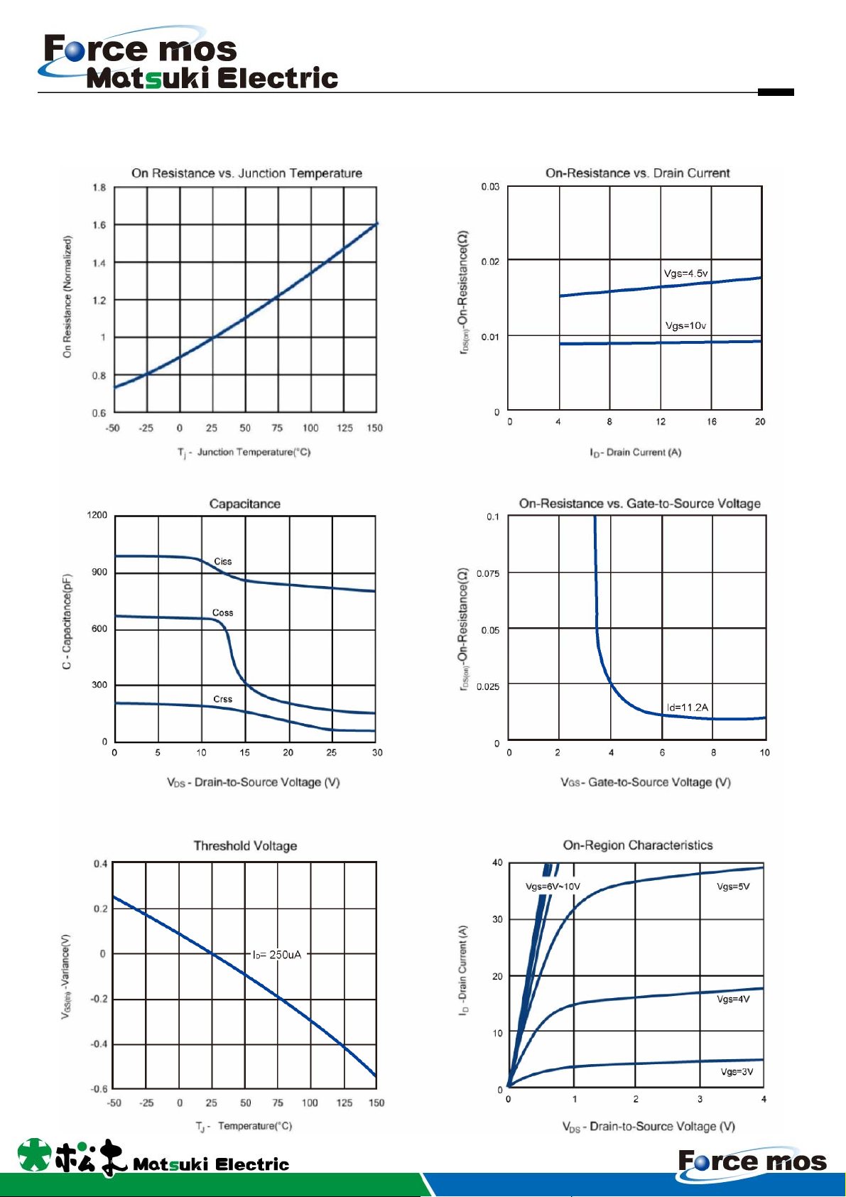
Typical Characteristics (TJ =25℃ Noted)
ug, 2011-Ver1.0
Jul, 2012-Ver1.3
03

A
Dual N-Channel 30-V(D-S) MOSFET
Typical Characteristics (TJ =25℃ Noted)
ME4932A/ME4932A-G
ug, 2011-Ver1.0
Jul, 2012-Ver1.3
04

A
FET2
ME4932A/ME4932A-G
Dual N-Channel 30-V(D-S) MOSFET
Electrical Characteristics (TA =25℃ Unless Otherwise Specified)
Symbol Parameter Limit Min Typ Max Unit
STATIC
GS=0V, ID=250μA
BVDSS Drain-Source Breakdown Voltage
VGS(th) Gate Threshold Voltage
IGSS Gate Leakage Current VDS=0V, VGS=±20V ±100 nA
IDSS Zero Gate Voltage Drain Current VDS=30V, VGS=0V 1
V
DS=VGS, ID=250μA
V
30 V
1 3 V
μA
RDS(ON)
Drain-Source On-State Resistance
a
VSD Diode Forward Voltage IS=9A, VGS=0V 0.83 1.5 V
DYNAMIC
Qg Total Gate Charge VDS=15V, VGS=10V, ID=9A
Qg Total Gate Charge
Qgs Gate-Source Charge
Qgd Gate-Drain Charge
Ciss Input capacitance 725
Coss Output Capacitance 114
Crss Reverse Transfer Capacitance
Rg Gate-Resistance VDS=0V, V
td(on)
tr
td(off)
tf
Turn-On Delay Time
Turn-On Rise Time
Turn-Off Delay Time
Turn-Off Fall Time
VGS=10V, ID= 9A 13 15.8
V
GS=4.5V, ID= 7A 17.5 23
18.4
9.3
4.4
4
13.6
8.9
38.4
5.9
V
DS=15V, VGS=4.5V, ID=9A
V
DS=15V, VGS=0V, f=1.0MHz
=0V, f=1MHz 1.5
GS
V
DD=15V, RL =3Ω
I
D=1A, VGEN=10V
R
G=3Ω
36
mΩ
nC
pF
Ω
ns
Notes: a. Pulse test: pulse width≦ 300us, duty cycle≦ 2%, Guaranteed by design, not subject to production testing.
b. Matsuki Electric/ Force mos reserves the right to improve product design, functions and reliability without notice.
ug, 2011-Ver1.0
Jul, 2012-Ver1.3
05

A
Dual N-Channel 30-V(D-S) MOSFET
Typical Characteristics (TJ =25℃ Noted)
ME4932A/ME4932A-G
ug, 2011-Ver1.0
Jul, 2012-Ver1.3
06

A
Dual N-Channel 30-V(D-S) MOSFET
Typical Characteristics (TJ =25℃ Noted)
ME4932A/ME4932A-G
ug, 2011-Ver1.0
Jul, 2012-Ver1.3
07

A
Dual N-Channel 30-V(D-S) MOSFET
ME4932A/ME4932A-G
SOP-8 Package Outline
DIM
MILLIMETERS (mm)
MIN MAX
A 1.35 1.75
A1 0.10 0.25
B 0.35 0.49
C 0.18 0.25
D 4.80 5.00
E 3.80 4.00
e 1.27 BSC
H 5.80 6.20
L 0.40 1.25
θ 0° 7°
ote: 1. Refer to JEDEC MS-012AA.
2. Dimension “D” does not include mold flash, protrusions
or gate burrs . Mold flash, protrusions or gate burrs shall not
ug, 2011-Ver1.0
Jul, 2012-Ver1.3
exceed 0.15 mm per side.
08

 Loading...