

Page 1
®
HIGH VOLTAGE ULTRA-FAST DIODE FOR VIDEO
MAJOR PRODUCT CHARACTE RISTICS
MDV04-600
I
Fpeak
V
RRM
t
rr
(max) 1.2 V
V
F
4 A
600 V
55 ns
FEATURES AND BENE FITS
TURBOSWITCH TM OUTSTANDING BENEFITS.
HIGH REVERSE VO LTAGE : 600 V
LOW POWER LOSSES INDUCING LOW
TEMPERATURE A ND HIGH RELIABILITY.
OPTIMIZED TRADE-OFF BETWEEN trr AND
SOFTNESS FOR VIDEO HORIZONTAL
DEFLECTION.
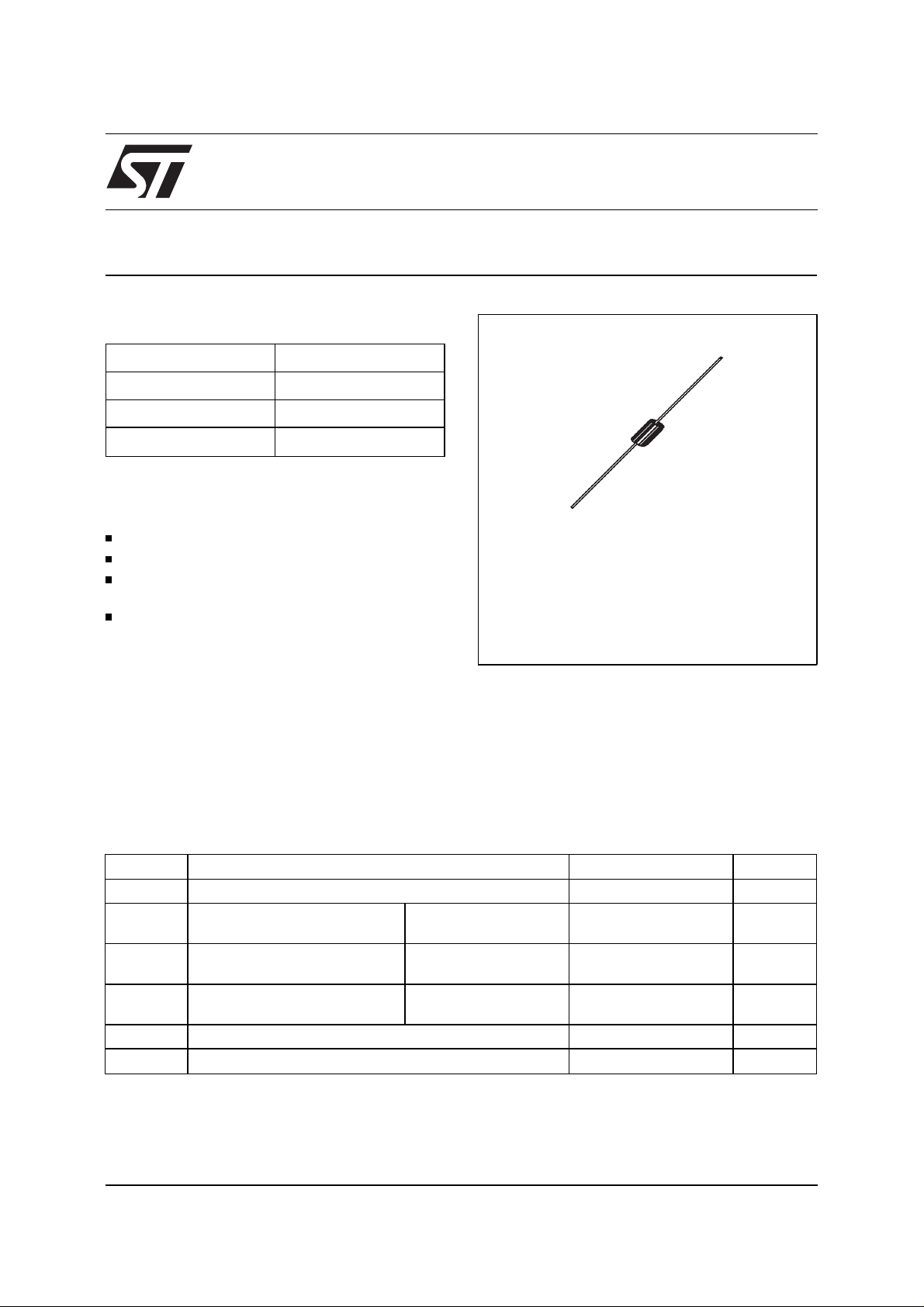
DESCRIPTION
High voltage ultra-fast diode especially designed
for modulation and flyback rectification in standard
and high resolution displays for TV’s and monitors.
The device is packaged in a DO-201AD axial
enveloppe.
DO-201AD
(plastic)
ABSOLUTE RATINGS
(limiting values)
Symbol Parameter VALUE Unit
V
RRM
peak Forward peak current (1)
I
F
Repetitive peak reverse voltage 600 V
δ
=0.5 Ta=115°C
4A
triangular
I
FRM
I
FSM
Repetitive peak forward
current
Surge non repetitive forward
tp=5µs
100 A
F=1kHz square
tp = 10 ms sinusoidal 80 A
current
T
stg
T
j
Storage temperature range
- 40 to 150 °C
Maximum operating junction temperature 150 °C
(1) on infinite heatsink with 10mm lead length
August 1999 - Ed: 4A
1/4
Page 2
MDV04-600
THERMAL RE SISTA NC ES
Symbol Parameter Max. Unit
R
th(j-l)
R
th(j-a)
Junction to lead 20
Junction to ambient on printed circuit L lead = 10mm 75
STATIC ELECTRICAL CHARACTER ISTICS
Symbol Parameter Test Conditions Typ. Max. Unit
*
I
R
V
** Forward voltage drop IF = 4 A Tj = 25°C
F
Reverse leakage current V
= 480V Tj = 25°C
R
Tj = 125°C
Tj = 125°C
50
0.75
1.28
1.20
Pulse test : * tp = 5 ms, δ < 2%
**tp = 380 µs, δ < 2%
DYNAMIC ELECTRICAL CHARACTE RISTICS
TURN-OFF SWITCHING
Symbol Parameter Test Conditions Typ. Max. Unit
t
rr
Reverse rec overy tim e IF = 0.5A IR = 1A
55 75 ns
Irr = 0.25A
= 100 mA IR = 100 mA
I
F
130 ns
Irr = 10mA
°
C/W
°
C/W
µ
mA
A
V
V
DYNAMIC ELECTRICAL CHARACTERIS TICS
TURN-ON SWITCHING
Symbol Parameter Test Conditions Typ. Max. Unit
t
fr
V
FP
Forward rec overy time IF = 4 A dIF/dt = 100 A/µs
Peak forward voltage 15 V
Measured at1.1 x V
Tj = 25°C
max.
F
0.5
To evaluate the maximum conduction losses use the following equation :
x I
1.0
P
=
δ
: duty cycle
: Peak current
I
p
Ex : for I
2/4
p
2
= 4 A and δ = 0.5, P = 1.2 Watts.
p
x
δ +
0.050
2
x I
p
x δ
3
µ
s
Page 3

MDV04-600
Fig. 1:
Power dissipation versus peak forward cur-
rent (triangular waveform, δ=0.5).
PF(av)(W)
1.4
1.2
1.0
0.8
0.6
0.4
0.2
0.0
0.0 0.5 1.0 1.5 2.0 2.5 3.0 3.5 4.0 4.5
Fig. 3:
Forward voltage drop versus forward cur-
Ip(A)
rent (maximum values).
IFM(A)
1E+2
1E+1
1E+0
1E-1
1E-2
0.0 0.2 0.4 0.6 0.8 1.0 1.2 1.4 1.6 1.8 2.0 2.2 2.4 2.6 2.8
Tj=125°C
Tj=25°C
VFM(V)
Fig. 2:
Relative variation of thermal impedance
junction to ambient versus pulse duration (epoxy
printed circuit board, e(Cu)=35µm), recommended
pad layout).
K=[Zth(j-a)/Rth(j-a)]
1E+0
δ = 0.5
δ = 0.2
1E-1
δ = 0.1
1E-2
Single pulse
t(s)
1E-3
1E-3 1E-2 1E-1 1E+0 1E+1 1E+2 1E+3
Fig. 4:
Reverse rec overy tim e vers us dIF/ dt.
trr(ns)
400
350
300
250
200
150
100
50
0
0 20 40 60 80 100 120 140 160 180 200
dIF/dt(A/µs)
T
=tp/T
δ
IF=Ip
90% confidence
Tj=125°C
tp
Fig. 5:
Transient peak forward voltage versus
dIF/dt.
VFP(V)
20
IF=Ip
90% confidence
Tj=125°C
15
10
5
dIF/dt(A/µs)
0
0 20 40 60 80 100 120 140 160 180 200
Fig. 6:
Forward rec over y time versus dIF/dt.
tfr(ns)
350
300
250
IF=Ip
90% confidence
Tj=125°C
Vfr=1.5V
200
150
100
50
0
0 20 40 60 80 100 120 140 160 180 200
dIF/dt(A/µs)
3/4
Page 4

MDV04-600
PACKAGE ME CHANICAL D AT A
DO-201AD
BA
B
ØC
note 1
ØD ØD
DIMENSIONS
REF.
Millimeters Inches
Min. Max. Min. Max.
A 9.50 0.374
B 25.40 1.000
∅ C 5.30 0.209
∅ D 1.30 0.051
E 1.25 0.049
E
note 2
note 1
E
NOTES
1 - The lead diameter ∅ D is not controlled over zone E
2 - The minimum axial length within which the device may be
placed with its leads bent at right angles is 0.59"(15 mm)
Ordering type Marking Package Weight Base qty Delivery mode
MDV04-600 MDV04-600 DO-201AD 1.166g. 600 Ammopack
MDV04-600RL MDV04-600 DO-201AD 1.166g. 1900 Tape & reel
Epoxy meets UL94,V0
Polarity : Cathode indicated by polarity band
Information furnished is believed to be accurate and reliable. However, STMicroelectronics assumes no responsibility for the consequences of
use of such information nor for any infringement of patents or other rights of third parties which may result from its use. No license is granted by
implication or ot herwise un der an y patent or patent ri ghts of STMicroel ectr onics. Spec ificati ons mentioned in this public ation a re subj ect to
change without notice. This publication supersedes and replaces all information previously supplied.
STMicroelectronics products are not authorized for use as critical components in l i fe s upport devices or systems without express written approval of STMicroelectronics.
The ST logo is a registered trademark of STMicr oelectroni cs
© 1999 STMicroelectronics - Printed in Italy - All rights reser ved.
STMicroelectronics GROUP OF COMPANIES
Australia - Brazil - China - Finland - France - Germany - Hong Kong - India - Italy - Japan - Malaysia
Malta - Morocco - Singapore - Spain - Sweden - Switzerland - United Kingdom - U.S.A.
http://www.st.com
4/4
 Loading...