

Page 1
MDV03-400
ULTRA-FAST RECOVERY DIODE
MAJOR PROD UCTS CHARACTE RIST ICS
I
F(AV)
V
RRM
t
rr
(max) 1.4 V
V
F
3 A
400 V
25 ns
PRELIMINARY DATASHEET
FEATURES
VERY LOW RE VE RS E RE CO VERY T IME
VERY LOW SWITCHING LOSSES
LOW NOI S E TURN-OFF S W I TC HING
DESCRIPTION
Ultra-fast diode especially designed f or modulation
and flyback rectification in standard and high reso-
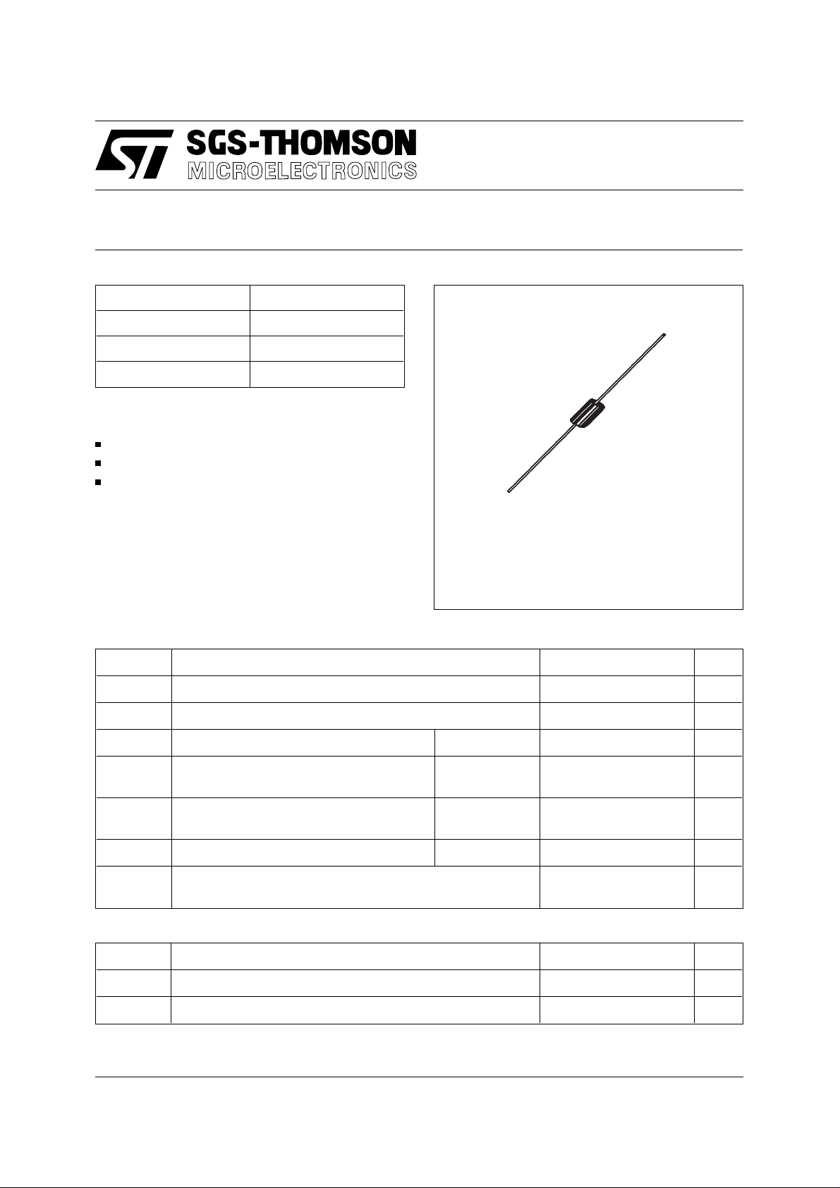
DO-201AD
(Plastic)
lution displays for TV’s and monitors.
The device is packaged in a DO-201AD axial enveloppe.
ABSOLUTE RAT I NG S (limiting v alues)
Symbol Parameter Value Unit
V
RRM
V
RSM
I
FRM
I
F (AV)
Repetitive peak reverse voltage 400 V
Non repetitive peak reverse voltage 440 V
Repetive peak forward current tp ≤ 10µs60A
Average forward current* T
a =
65°C
3A
δ = 0.5
I
FSM
Surge non repetitive forwar d current tp = 10ms
60 A
Sinusoidal
P
T
stg
T
Power dissipation * T
Storage and junction temperature range
j
a =
65°C
4.2 W
- 40 to + 150
- 40 to + 150
THERMAL RES IST ANCE S
Symbol Parameter Value Unit
R
th (j - l)
R
th (j - a)
Junction to lead 20 °C/W
Junction to ambient on printed circuit L lead = 10mm 75 °C/W
* On infinite heatsink with 10mm lead lengh.
September 1996 - Ed: 2
°C
1/3
Page 2
MDV03-400
STATIC ELECTRI CAL CHARACTERISTICS
Symbol Parameter Test Conditions Typ. Max. Unit
* Reverse Leakage Current VR = V
I
R
**
V
F
Forward Voltage Drop I
RRM
= 3 A Tj = 25°C
F
Tj = 25° C
Tj = 100°C
Tj = 100°C
20
0.5
1.5
1.4
Pulse test : *tp= 5 m s, δ < 2%
**tp = 38 0 µs, δ < 2%
DYNAMIC EL EC TRICAL CHARACT E RIS TICS
TURN-OFF S W I TCH ING
Symbol Parameter Test Co n d ition s Typ. Max. Unit
t
rr
Reverse Rec overy Tim e IF=1A diF/dt= -15A/µs
V
= 30V
R
= 0.5A IR = 1A Irr = 0.25A 25 ns
I
F
55 ns
DYNAMIC EL EC TRICAL CHARACT E RIS TICS
TURN-ON SW ITCHING
Symbol Parameter Test Co n d ition s Typ. Max. Unit
t
fr
V
FP
Forward Recovery Time IF = 3 A dIF/dt = 60 A/µ s
Peak Forward Voltage 13 V
Measured at 1.1 V
Tj = 25°C
max.
F
250 ns
µA
mA
V
V
To evaluate the maximum con duction losses use the fo llowing equation :
1.10
P
=
x I
2
p
x
δ +
0.050
x I
3
^ 2
p
x δ
δ : duty c ycle
: Peak current
I
p
Ex : for I
= 3 A and δ = 0.5, P = 0.9 Watts .
p
2/3
Page 3
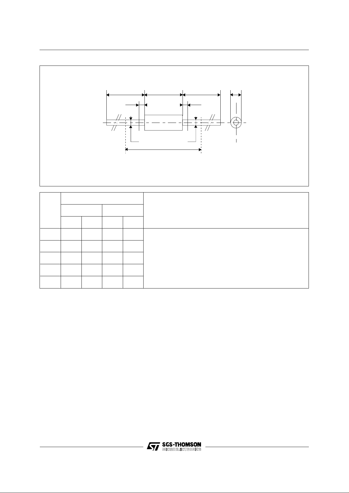
PACKAGE MECHANICAL DATA
DO-201A D (Pl astic)
MDV03-400
BA B
note 1
/
O
DIMENSI O NS
REF.
Millimeters Inches
Min. Max. Min. Max.
A 9.50 0.374
B 25.40 1.000
∅ C 5.30 0.209
/
O
C
E
D
note 2
E
note 1
O
/
D
NOTES
1 - The lead diam eter ∅ D is not controlled over zone E
2 - The minimum axial lengh within which the device may be
placed with its leads bent at right angles is 0.59"(15 mm)
∅ D 1.30 0.051
E 1.25 0.049
Weight : 1 g
Marking : Type number - Date code
White band indicated cathode
cooling methode : by convertion ( method A)
Information furnished is believed to be accurate and reliable. However, SGS-THOMSON Microelectronics assumes no responsability for the
consequences of use of such information nor for any infringement of patents or other rights of third parties which may result from its use. No
license is granted by implication or otherwise under any patent or patent rights of SGS-THOMSON Microelectronics. Specifications mentioned
in this publication are subject to change without notice. This publication supersedes and replaces all information previously supplied.
SGS-THOMSON Microelectronics products are not authorized for use as critical components in life s upport devic es or systems without ex press
written approval of SGS-THOMSON Microelectronics.
© 1996 SGS-THOMSON Microelectronics - Printed in Italy - All rights reserved.
SGS-THOMSON Microelectronics GROUP OF COMPANIES
Australia - Brazil - Canada - China - France - Germany - Hong Kon g - Italy - Japan - Korea - Malaysia - Malt a - Morocco -
The Netherlands - Singapore - Spain - Sweden - Switzerland - Taiwan - Thailand - United Kingdom - U.S.A.
3/3
 Loading...