

Page 1
LOW INPUT CURRENT
PHOTOTRANSISTOR OPTOCOUPLERS
MCT5200 MCT5201 MCT5210 MCT5211
Description
The MCT52XX series consists of a high-efficiency AlGaAs, infrared emitting
diode, coupled with an NPN phototransistor in a six pin dual-in-line package.
The MCT52XX is well suited for CMOS to LSTT/TTL interfaces, offering
250% CTR
CE(SAT)
with 1 mA of LED input current. When an LED input
current of 1.6 mA is supplied data rates to 20K bits/s are possible.
The MCT52XX can easily interface LSTTL to LSTTL/TTL, and with use of an
external base to emitter resistor data rates of 100K bits/s can be achieved.
Features
• High CTR
• CTR guaranteed 0°C to 70°C
• High common mode transient rejection 5kV/µs
• Data rates up to 150 kbits/s (NRZ)
• Underwriters Laboratory (UL) recognized (file #E90700)
• VDE recognized (file #94766)
– Add option 300 (e.g., MCT5211.300)
comparable to Darlingtons
CE(SAT)
6
1
6
1
6
1
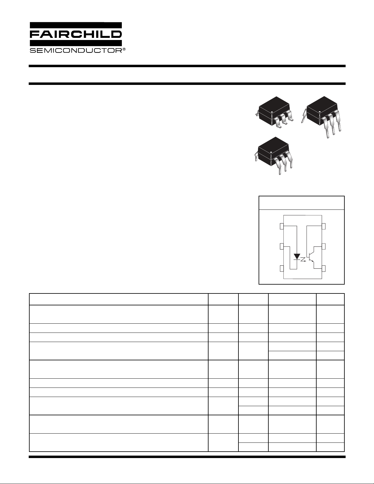
SCHEMATIC
ANODE
1
6
BASE
Applications
• CMOS to CMOS/LSTTL logic isolation
CATHODE
• LSTTL to CMOS/LSTTL logic isolation
• RS-232 line receiver
• Telephone ring detector
• AC line voltage sensing
• Switching power supply
Parameters Symbol Device Value Units
TOTAL DEVICE
Storage Temperature T
Operating Temperature T
Lead Solder Temperature T
Total Device Power Dissipation @ 25°C (LED plus detector)
Derate Linearly From 25°C 3.5 mW/°C
STG
OPR
SOL
P
D
All -55 to +150 °C
All -55 to +100 °C
All 260 for 10 sec °C
All
EMITTER
Continuous Forward Current I
Reverse Input Voltage V
Forward Current - Peak (1 µs pulse, 300 pps) I
LED Power Dissipation
Derate Linearly From 25°C All 1.0 mW/°C
F
R
(pk) All 3.0 A
F
P
D
All 50 mA
All 6 V
All 75 mW
DETECTOR
Continuous Collector Current I
Detector Power Dissipation
Derate Linearly from 25°C All 2.0 mW/°C
C
P
D
All 150 mA
All 150 mW
2
3
260 mW
COL
5
4 EMITTER
© 2003 Fairchild Semiconductor Corporation
Page 1 of 11
6/10/03
Page 2

∆
∆
Ω
LOW INPUT CURRENT
PHOTOTRANSISTOR OPTOCOUPLERS
MCT5200 MCT5201 MCT5210 MCT5211
(T
ELECTRICAL CHARACTERISTICS
INDIVIDUAL COMPONENT CHARACTERISTICS
Parameters Test Conditions Symbol Device Min Typ** Max Units
EMITTER
Input Forward Voltage (I
Forward Voltage Temp.
Coefficient
Reverse Voltage (I
Junction Capacitance (V
DETECTOR
Collector-Emitter Breakdown Voltage (I
Collector-Base Breakdown Voltage (I
Emitter-Base Breakdown Voltage (I
Collector-Emitter Dark Current (V
Capacitance Collector to Emitter (V
Collector to Base (V
Emitter to Base (V
= 5 mA) V
F
(I
= 2 mA)
F
= 10 µA) V
R
= 0 V, f = 1.0 MHz) C
F
= 1.0 mA, I
C
= 10 µA, I
C
= 10 µA, I
C
CE
CE
CB
EB
= 25°C Unless otherwise specified.)
A
= 0) BV
F
= 0) BV
F
= 0) BV
F
= 10V, I
= 0, R
F
= 1M Ω )I
BE
CER
= 0, f = 1 MHz) C
= 0, f = 1 MHz) C
= 0, f = 1 MHz) C
F
V
F
T
A
R
J
CEO
CBO
EBO
CE
CB
EB
All 1.25 1.5 V
All -1.75
mV/
°C
All 6 V
All 18 pF
All 30 100 V
All 30 120 V
All 5 10 V
All 1 100 nA
All 10 pF
All 80 pF
All 15 pF
ISOLATION CHARACTERISTICS
Characteristic Test Conditions Symbol Device Min Typ** Max Units
Input-Output Isolation
(10)
Voltage
Isolation Resistance
Isolation Capacitance
(10)
(9)
Common Mode Transient V
Rejection – Output High V
Common Mode Transient V
Rejection – Output Low V
**All typical T
=25°C
A
(f = 60Hz, t = 1 min.) V
V
= 500 VDC, T
I-O
V
= 0, f = 1 MHz C
I-O
= 50 V
CM
CM
CM
CM
= 50 V
= 50 V
= 50 V
P-P1
P-P
P-P1
P-P1
= 25°CR
A
, R
, R
, R
, R
= 750 Ω , I
L
= 1K Ω , I
L
= 750 Ω , I
L
= 1K Ω , I
L
= 0
F
= 0 MCT5200/01
F
=1.6mA
F
= 5 mA MCT5200/01
F
CM
CM
ISO
ISO
ISO
H
L
All 5300 Vac(rms)
All 10
11
All 0.7 pF
MCT5210/11
MCT5210/11
5000 V/µs
5000 V/µs
© 2003 Fairchild Semiconductor Corporation
Page 2 of 11
6/10/03
Page 3

LOW INPUT CURRENT
PHOTOTRANSISTOR OPTOCOUPLERS
MCT5200 MCT5201 MCT5210 MCT5211
TRANSFER CHARACTERISTICS
(T
= 0°C to 70°C Unless otherwise specified.)
A
DC Characteristics Test Conditions Symbol Device Min Typ** Max Units
I
Saturated Current
Transfer Ratio
(1)
(Collector to Emitter)
Current Transfer Ratio
(Collector to Emitter)
Current Transfer Ratio
Collector to Base(2)
Saturation Voltage
= 10 mA, V
F
= 5 mA, V
I
F
I
= 3.0 mA, V
F
I
= 1.6 mA, V
F
I
= 1.0 mA, V
F
I
= 3.0 mA, V
F
= 1.6 mA, V
(1)
F
I
= 1.0 mA, V
F
I
= 10 mA, V
F
= 5 mA, V
I
F
I
= 3.0 mA, V
F
I
= 1.6 mA, VCE = 4.3 V
F
I
= 1.0 mA, VCE = 4.3 V 0.25
F
I
= 10 mA, ICE = 7.5 mA
F
= 5 mA, ICE = 6 mA MCT5201 0.4
I
F
= 3.0 mA, ICE = 1.8 mA MCT5210 0.4
I
F
I
= 1.6 mA, ICE = 1.6 mA MCT5211 0.4
F
= 0.4 V
CE
= 0.4 V MCT5201 120
CE
= 0.4 V MCT5210 60
CE
= 0.4 V
CE
= 0.4 V 75
CE
= 5.0 V
CE
= 5.0 V
CE
= 5.0 V 110
CE
= 4.3 V
CB
= 4.3 V MCT5201 0.28
CB
= 4.3 V MCT5210 0.2
CE
CTR
CTR
CTR
CE(SAT)
(CE)
(CB)
MCT5200 75
MCT5211
MCT5210 70
MCT5211
MCT5200 0.2
MCT5211
MCT5200 0.4
V
CE(SAT)
100
150
0.3
%
%I
%
V
AC Characteristics Test Conditions Symbol Device Min Typ Max Units
Propagation Delay
High to Low
Propagation Delay
Low to High
Delay Time
Rise Time
(3)
(4)
(5)
(6)
RL = 330 Ω, RBE = ∞ IF = 3.0 mA
R
= 3.3 kΩ, R
L
R
= 750 Ω, RBE = ∞ IF = 1.6mA
L
R
= 4.7 kΩ, RBE = 91 kΩ V
L
R
= 1.5 kΩ, RBE = ∞ IF = 1.0mA 17
L
= 10 kΩ, RBE = 160 kΩ VCC = 5.0V 24
R
L
= 0.4V, VCC = 5V,
V
CE
R
= fig. 13, RBE = 330 kΩ
L
= 39 kΩ VCC = 5.0 V 7
BE
= 5.0V 15
CC
= 10mA MCT5200 1.6 12
I
F
I
= 5mA MCT5201 3 30
F
T
PHL
RL = 330 Ω, RBE = ∞ IF = 3.0 mA
= 3.3 kΩ, R
R
L
R
= 750 Ω, R
L
R
= 4.7 kΩ, R
L
R
= 1.5 kΩ, R
L
R
= 10 kΩ, R
L
= 0.4V, VCC = 5V,
V
CE
R
= fig. 13, RBE = 330 kΩ
L
VCE = 0.4V,
R
= 330 kΩ,
BE
R
= 1 kΩ, VCC = 5V
L
VCE = 0.4V,
R
= 330 kΩ,
BE
R
= 1 kΩ, VCC = 5V
L
= 39 kΩ VCC = 5.0 V 8
BE
= ∞ IF = 1.6mA
BE
= 91 kΩ VCC = 5.0V 11
BE
= ∞ IF = 1.0mA 7
BE
= 160 kΩ VCC = 5.0 V 16
BE
= 10mA MCT5200 18 20
I
F
I
= 5mA MCT5201 12 13
F
= 10mA
I
F
I
= 5mA MCT5201 1.1 15
F
= 10mA
I
F
I
= 5mA MCT5201 2.5 20
F
T
PLH
t
d
t
r
MCT5210
MCT5211
MCT5210
MCT5211
MCT5200 0.5 7
MCT5200 1.3 6
10
14
µs
0.4
2.5
µs
µs
µs
© 2003 Fairchild Semiconductor Corporation
Page 3 of 11
6/10/03
Page 4

LOW INPUT CURRENT
PHOTOTRANSISTOR OPTOCOUPLERS
MCT5200 MCT5201 MCT5210 MCT5211
TRANSFER CHARACTERISTICS (T
= 0°C to 70°C Unless otherwise specified.) (Continued)
A
DC Characteristics Test Conditions Symbol Device Min Typ** Max Units
Storage Time
Fall Time
(8)
(7)
VCE = 0.4V,
R
= 330 kΩ,
BE
R
= 1 kΩ, VCC = 5V
L
VCE = 0.4V,
R
= 330 kΩ,
BE
R
= 1 kΩ, VCC = 5V
L
= 10mA
I
F
I
= 5mA MCT5201 10 13
F
= 10mA
I
F
I
= 5mA MCT5201 16 30
F
t
s
t
f
MCT5200 15 18
MCT5200 16 30
µs
µs
**All typicals at TA = 25°C
Notes
1. DC Current Transfer Ratio (CTR
100%, at a specified voltage between the collector and emitter (V
2. The collector base Current Transfer Ratio (CTR
input LED current (I
) time 100%.
F
3. Referring to Figure 14 the T
) is defined as the transistor collector current (ICE) divided by the input LED current (IF) x
CE
) is defined as the transistor collector base photocurrent(ICB) divided by the
CB
propagation delay is measured from the 50% point of the rising edge of the data input pulse to
PHL
CE
).
the 1.3V point on the falling edge of the output pulse.
4. Referring to Figure 14 the T
propagation delay is measured from the 50% point of the falling edge of data input pulse to the
PLH
1.3V point on the rising edge of the output pulse.
5. Delay time (t
6. Rise time (t
7. Storage time (t
8. Fall time (t
9. C
is the capacitance between the input (pins 1, 2, 3 connected) and the output, (pin 4, 5, 6 connected).
ISO
) is measured from 50% of rising edge of LED current to 90% of Vo falling edge.
d
) is measured from 90% to 10% of Vo falling edge.
r
) is measured from 50% of falling edge of LED current to 10% of Vo rising edge.
s
) is measured from 10% to 90% of Vo rising edge.
f
10. Device considered a two terminal device: Pins 1, 2, and 3 shorted together, and pins 5, 6 and 7 are shorted together.
© 2003 Fairchild Semiconductor Corporation
Page 4 of 11
6/10/03
Page 5

LOW INPUT CURRENT
PHOTOTRANSISTOR OPTOCOUPLERS
MCT5200 MCT5201 MCT5210 MCT5211
TYPICAL PERFORMANCE GRAPHS
Fig. 1 LED Forward Voltage vs. Forward Current Fig. 2 Normalized Current Transfer Ratio vs.
2.0
1.8
1.6
1.4
TA = -55°C
1.2
TA = 25°C
- FORWARD VOLTAGE (V)
1.0
F
V
0.8
0.1 1 10
TA = 100°C
100 0.1
IF - LED FORWARD CURRENT (mA)
Fig. 3 Normalized CTR vs. Temperature
1.6 10
Normalized to:
= 5mA
I
1.4
F
= 5V
V
CE
= 25°C
T
CE
A
1.2
1.0
0.8
0.6
0.4
NORMALIZED CTR
0.2
0.0
-60 -40 -20 0 20 40 60 80 100
IF = 1mA
IF = 0.5 mA
IF = 0.2 mA
- AMBIENT TEMPERATURE - °C
T
A
IF = 10mA
= 2mA
I
F
= 5mA
I
F
- COLLECTOR
CE
- EMITTER CURRENT
NORMALIZED I
0.0001
1.2
1.0
CE
0.8
0.6
0.4
NORMALIZED CTR
0.2
0
1
0.1
0.01
0.001
0.1 1 10
V
- COLLECTOR - EMITTER VOLTAGE - V
CE
Forward Current
Normalized to:
= 5mA
I
F
= 5V
V
CE
= 25°C
T
A
110
I
- FORWARD CURRENT (mA)
F
Fig. 4 Normalized Collector vs.
Collector - Emitter Voltage
IF = 10 mA
IF = 5 mA
IF = 2 mA
IF = 1 mA
IF = 0.5 mA
IF = 0.2 mA
Normalized to:
= 5mA
I
F
V
T
= 5V
CE
= 25°C
A
:
100
Fig. 5 Normalized Collector Base Photocurrent
Ratio vs. Forward Current
100
10
1
0.1
BASE PHOTO CURRENT
NORMALIZED ICB - COLLECTOR
0.01
0.1 1 10010
I
- FORWARD CURRENT - mA
F
© 2003 Fairchild Semiconductor Corporation
Normalized to:
= 5mA
I
F
= 4.3V
V
CB
= 25°C
T
A
Page 5 of 11
Fig. 6 Normalized Collector Base Current vs. Temperature
10
IF = 10 mA
1
0.1
BASE CURRENT
0.01
Normalized to:
= 5mA
I
F
= 4.3V
V
NORMALIZED - COLLECTOR
CB
= 25°C
T
A
0.001
-60 -40 -20 0 20 40 60 80 100
T
- AMBIENT TEMPERATURE - °C
A
IF = 5 mA
IF = 1 mA
IF = 0.5 mA
IF = 0.2 mA
IF = 2 mA
6/10/03
Page 6

LOW INPUT CURRENT
PHOTOTRANSISTOR OPTOCOUPLERS
MCT5200 MCT5201 MCT5210 MCT5211
TYPICAL PERFORMANCE GRAPHS (Continued)
Fig. 7 Collector-Emitter Dark Current vs.
Ambient Temperature
10000
IF = 0mA
V
= 10V
CE
1000
100
10
- DARK CURRENT (nA)
1
CEO
I
0.1
0 102030405060708090
TA - AMBIENT TEMPERATURE (°C) TA - AMBIENT TEMPERATURE (°C)
Fig. 9 Switching Time vs.
25
IF = 10mA
V
CC
R
L
20
R
BE
15
10
5
SWITCHING TIME - t(µs)
0
-60 -40 -20 0 20 40 60 80 100
Ambient Temperature
= 5V
= 1K
= 100K
Refer to Figure 13 for switching time circuit
t
PLH
t
r
t
t
PHL
T
- AMBIENT TEMPERATURE (°C)
A
d
t
s
t
f
100
Fig. 8 Switching Time vs.
Ambient Temperature
30
IF = 10mA
= 5V
V
CC
25
= 1K
R
L
= 330K
R
BE
20
15
10
SWITCHING TIME - t(µs)
5
0
-60 -40 -20 0 20 40 60 80 100
Refer to Figure 13 for switching time circuit
t
PLH
t
f
t
t
r
t
PHL
d
t
s
Fig. 10 Switching Time vs.
Ambient Temperature
30
IF = 5mA
= 5V
V
CC
25
= 1K
R
L
= 330K
R
BE
20
15
10
SWITCHING TIME - t(µs)
5
0
-60 -40 -20 0 20 40 60 80 100
Refer to Figure 13 for switching time circuit
t
f
t
PLH
t
s
t
t
r
t
PHL
d
TA - AMBIENT TEMPERATURE (°C)
Fig. 11 Switching Time vs.
Ambient Temperature
20
15
IF = 5mA
= 5V
V
CC
= 1K
R
L
= 100K
R
BE
Refer to Figure 13 for switching time circuit
10
5
SWITCHING TIME - t(µs)
0
-60 -40 -20 0 20 40 60 80
t
PHL
T
- AMBIENT TEMPERATURE (°C) BASE RESISTANCE - RBE (kΩ)
A
t
t
r
© 2003 Fairchild Semiconductor Corporation
t
d
PLH
Fig. 12 Turn-on Time vs.
Base-Emitter Resistance
100
t
, IF=3mA, RL=3.3K
= 0.4V
CE
= 25°C
A
PLH
t
, IF=1.6mA, RL=4.7K
PLH
t
, IF=1mA, RL=10K
PLH
t
, IF=1mA, RL=10K
PHL
t
, IF=1.6mA, RL=4.7K
PHL
t
, IF=3mA, RL=3.3K
PHL
6/10/03
(µs)
PLH
, t
t
f
t
s
100
PHL
10
VCC = 5V
V
T
SWITCHING TIME - t
1
10 100 1000 10000
Page 6 of 11
Page 7

LOW INPUT CURRENT
PHOTOTRANSISTOR OPTOCOUPLERS
MCT5200 MCT5201 MCT5210 MCT5211
TYPICAL ELECTRO-OPTICAL CHARACTERISTICS (TA = 25°C Unless Otherwise Specified)
= 5.0 V
V
CC
330K
t
PHL
TEST CIRCUIT
1K 4.7K
D1
V
O
, t
PLH
D2
D3
D4
Pulse Gen
ZO = 50Ω
f = 10KHz
10% D.F.
I
monitor
F
100 Ω
t
, tf, td, t
r
TEST CIRCUIT
s
330K
VCC = 5.0 V
1K
V
O
Pulse Gen
ZO = 50Ω
f = 10KHz
10% D.F.
monitor
I
F
100 Ω
INPUT
(I
F
0
OUTPUT
(V
)
O
0
Figure 13.
50%
)
t
d
90%
t
PHL
t
1.3 V
10% 10%
t
r
Figure 14. Switching Circuit Waveforms
PLH
1.3 V
t
s
90%
t
f
© 2003 Fairchild Semiconductor Corporation
Page 7 of 11
6/10/03
Page 8

LOW INPUT CURRENT
)
)
)
)
)
)
PHOTOTRANSISTOR OPTOCOUPLERS
MCT5200 MCT5201 MCT5210 MCT5211
Package Dimensions (Through Hole) Package Dimensions (Surface Mount)
0.350 (8.89)
0.330 (8.38)
3
2
5
4
0.070 (1.78)
0.045 (1.14)
Lead Coplanarity : 0.004 (0.10) MAX
1
6
PIN 1
ID.
0.020 (0.51)
MIN
0.100 (2.54)
TYP
0.270 (6.86)
0.240 (6.10)
0.300 (7.62)
TYP
0.016 (0.40) MIN
0.315 (8.00)
MIN
0.405 (10.30)
MAX
NE
A
0.070 (1.78)
TING PL
A
0.045 (1.14)
SE
0.200 (5.08)
0.115 (2.92)
0.154 (3.90)
0.100 (2.54)
0.022 (0.56)
0.016 (0.41)
0.100 (2.54)
TYP
0.350 (8.89)
0.330 (8.38)
PIN 1
ID.
0.020 (0.51)
MIN
0.016 (0.40)
0.008 (0.20)
0° to 15°
0.270 (6.86)
0.240 (6.10)
0.300 (7.62)
TYP
0.200 (5.08)
0.165 (4.18)
0.022 (0.56)
0.016 (0.41)
Package Dimensions (0.4” Lead Spacing) Recommended Pad Layout for
Surface Mount Leadform
0.016 (0.41)
0.008 (0.20)
0.270 (6.86)
0.240 (6.10)
0.350 (8.89)
0.330 (8.38)
0.070 (1.78)
0.045 (1.14)
0.200 (5.08)
0.135 (3.43)
SEATING PLANE
0.154 (3.90)
0.100 (2.54)
0.022 (0.56)
0.016 (0.41)
0.004 (0.10)
MIN
0.100 (2.54) TYP
Note
All dimensions are in inches (millimeters)
© 2003 Fairchild Semiconductor Corporation
0.016 (0.40)
0.008 (0.20)
0.400 (10.16)
TYP
0° to 15°
Page 8 of 11
0.415 (10.54
0.100 (2.54
0.295 (7.49
0.070 (1.78
0.060 (1.52
0.030 (0.76
6/10/03
Page 9

LOW INPUT CURRENT
PHOTOTRANSISTOR OPTOCOUPLERS
MCT5200 MCT5201 MCT5210 MCT5211
ORDERING INFORMATION
Option Order Entry Identifier Description
S .S Surface Mount Lead Bend
SD .SD Surface Mount; Tape and Reel
W .W 0.4" Lead Spacing
300 .300 VDE 0884
300W .300W VDE 0884, 0.4" Lead Spacing
3S .3S VDE 0884, Surface Mount
3SD .3SD VDE 0884, Surface Mount, Tape and Reel
MARKING INFORMATION
MCT5200
V XX YY K
43
Definitions
1 Fairchild logo
2 Device number
VDE mark (Note: Only appears on parts ordered with VDE
3
option – See order entry table)
4 Two digit year code, e.g., ‘03’
5 Two digit work week ranging from ‘01’ to ‘53’
6 Assembly package code
5
1
2
6
© 2003 Fairchild Semiconductor Corporation
Page 9 of 11
6/10/03
Page 10

LOW INPUT CURRENT
PHOTOTRANSISTOR OPTOCOUPLERS
MCT5200 MCT5201 MCT5210 MCT5211
Carrier Tape Specifications
4.85 ± 0.20
0.30 ± 0.05
13.2 ± 0.2
0.1 MAX
User Direction of Feed
NOTE
All dimensions are in inches (millimeters)
Reflow Profile (Black Package, No Suffix)
300
250
200
150
100
Temperature (°C)
50
0
0.5 1 1.5 2 2.5 3 3.5 4 4.5
0
225
°C peak
Ramp up = 3
Time (Minute)
Time above 183° C, 60–150 sec
°C/sec
4.0 ± 0.1
10.30 ± 0.20
215°C, 10–30 s
12.0 ± 0.1
4.0 ± 0.1
• Peak reflow temperature: 225° C (package surface temperature)
• Time of temperature higher than 183° C for 60–150 seconds
• One time soldering reflow is recommended
1.55 ± 0.05
Ø
1.75 ± 0.10
7.5 ± 0.1
9.55 ± 0.20
Ø
1.6 ± 0.1
16.0 ± 0.3
© 2003 Fairchild Semiconductor Corporation
Page 10 of 11
6/10/03
Page 11

LOW INPUT CURRENT
PHOTOTRANSISTOR OPTOCOUPLERS
MCT5200 MCT5201 MCT5210 MCT5211
DISCLAIMER
FAIRCHILD SEMICONDUCTOR RESERVES THE RIGHT TO MAKE CHANGES WITHOUT FURTHER NOTICE TO
ANY PRODUCTS HEREIN TO IMPROVE RELIABILITY, FUNCTION OR DESIGN. FAIRCHILD DOES NOT ASSUME
ANY LIABILITY ARISING OUT OF THE APPLICATION OR USE OF ANY PRODUCT OR CIRCUIT DESCRIBED HEREIN;
NEITHER DOES IT CONVEY ANY LICENSE UNDER ITS PATENT RIGHTS, NOR THE RIGHTS OF OTHERS.
LIFE SUPPORT POLICY
FAIRCHILD’S PRODUCTS ARE NOT AUTHORIZED FOR USE AS CRITICAL COMPONENTS IN LIFE SUPPORT DEVICES
OR SYSTEMS WITHOUT THE EXPRESS WRITTEN APPROVAL OF THE PRESIDENT OF FAIRCHILD SEMICONDUCTOR
CORPORATION. As used herein:
1. Life support devices or systems are devices or systems
which, (a) are intended for surgical implant into the body, or
(b) support or sustain life, and (c) whose failure to perform
when properly used in accordance with instructions for use
provided in the labeling, can be reasonably expected to
result in a significant injury of the user.
2. A critical component in any component of a life support
device or system whose failure to perform can be
reasonably expected to cause the failure of the life support
device or system, or to affect its safety or effectiveness.
© 2003 Fairchild Semiconductor Corporation
Page 11 of 11
6/10/03
 Loading...